EP1291932A2 - Dispositif semiconductur organique et sa procédé de fabrication - Google Patents
Dispositif semiconductur organique et sa procédé de fabrication Download PDFInfo
- Publication number
- EP1291932A2 EP1291932A2 EP02019125A EP02019125A EP1291932A2 EP 1291932 A2 EP1291932 A2 EP 1291932A2 EP 02019125 A EP02019125 A EP 02019125A EP 02019125 A EP02019125 A EP 02019125A EP 1291932 A2 EP1291932 A2 EP 1291932A2
- Authority
- EP
- European Patent Office
- Prior art keywords
- organic semiconductor
- semiconductor device
- electrode
- insulation film
- supporting substrate
- Prior art date
- Legal status (The legal status is an assumption and is not a legal conclusion. Google has not performed a legal analysis and makes no representation as to the accuracy of the status listed.)
- Withdrawn
Links
Images


Classifications
-
- C—CHEMISTRY; METALLURGY
- C23—COATING METALLIC MATERIAL; COATING MATERIAL WITH METALLIC MATERIAL; CHEMICAL SURFACE TREATMENT; DIFFUSION TREATMENT OF METALLIC MATERIAL; COATING BY VACUUM EVAPORATION, BY SPUTTERING, BY ION IMPLANTATION OR BY CHEMICAL VAPOUR DEPOSITION, IN GENERAL; INHIBITING CORROSION OF METALLIC MATERIAL OR INCRUSTATION IN GENERAL
- C23C—COATING METALLIC MATERIAL; COATING MATERIAL WITH METALLIC MATERIAL; SURFACE TREATMENT OF METALLIC MATERIAL BY DIFFUSION INTO THE SURFACE, BY CHEMICAL CONVERSION OR SUBSTITUTION; COATING BY VACUUM EVAPORATION, BY SPUTTERING, BY ION IMPLANTATION OR BY CHEMICAL VAPOUR DEPOSITION, IN GENERAL
- C23C16/00—Chemical coating by decomposition of gaseous compounds, without leaving reaction products of surface material in the coating, i.e. chemical vapour deposition [CVD] processes
- C23C16/44—Chemical coating by decomposition of gaseous compounds, without leaving reaction products of surface material in the coating, i.e. chemical vapour deposition [CVD] processes characterised by the method of coating
- C23C16/50—Chemical coating by decomposition of gaseous compounds, without leaving reaction products of surface material in the coating, i.e. chemical vapour deposition [CVD] processes characterised by the method of coating using electric discharges
- C23C16/505—Chemical coating by decomposition of gaseous compounds, without leaving reaction products of surface material in the coating, i.e. chemical vapour deposition [CVD] processes characterised by the method of coating using electric discharges using radio frequency discharges
- C23C16/509—Chemical coating by decomposition of gaseous compounds, without leaving reaction products of surface material in the coating, i.e. chemical vapour deposition [CVD] processes characterised by the method of coating using electric discharges using radio frequency discharges using internal electrodes
-
- C—CHEMISTRY; METALLURGY
- C23—COATING METALLIC MATERIAL; COATING MATERIAL WITH METALLIC MATERIAL; CHEMICAL SURFACE TREATMENT; DIFFUSION TREATMENT OF METALLIC MATERIAL; COATING BY VACUUM EVAPORATION, BY SPUTTERING, BY ION IMPLANTATION OR BY CHEMICAL VAPOUR DEPOSITION, IN GENERAL; INHIBITING CORROSION OF METALLIC MATERIAL OR INCRUSTATION IN GENERAL
- C23C—COATING METALLIC MATERIAL; COATING MATERIAL WITH METALLIC MATERIAL; SURFACE TREATMENT OF METALLIC MATERIAL BY DIFFUSION INTO THE SURFACE, BY CHEMICAL CONVERSION OR SUBSTITUTION; COATING BY VACUUM EVAPORATION, BY SPUTTERING, BY ION IMPLANTATION OR BY CHEMICAL VAPOUR DEPOSITION, IN GENERAL
- C23C16/00—Chemical coating by decomposition of gaseous compounds, without leaving reaction products of surface material in the coating, i.e. chemical vapour deposition [CVD] processes
- C23C16/44—Chemical coating by decomposition of gaseous compounds, without leaving reaction products of surface material in the coating, i.e. chemical vapour deposition [CVD] processes characterised by the method of coating
- C23C16/54—Apparatus specially adapted for continuous coating
- C23C16/545—Apparatus specially adapted for continuous coating for coating elongated substrates
-
- H—ELECTRICITY
- H10—SEMICONDUCTOR DEVICES; ELECTRIC SOLID-STATE DEVICES NOT OTHERWISE PROVIDED FOR
- H10K—ORGANIC ELECTRIC SOLID-STATE DEVICES
- H10K10/00—Organic devices specially adapted for rectifying, amplifying, oscillating or switching; Organic capacitors or resistors having potential barriers
- H10K10/40—Organic transistors
- H10K10/46—Field-effect transistors, e.g. organic thin-film transistors [OTFT]
- H10K10/462—Insulated gate field-effect transistors [IGFETs]
- H10K10/464—Lateral top-gate IGFETs comprising only a single gate
-
- H—ELECTRICITY
- H10—SEMICONDUCTOR DEVICES; ELECTRIC SOLID-STATE DEVICES NOT OTHERWISE PROVIDED FOR
- H10K—ORGANIC ELECTRIC SOLID-STATE DEVICES
- H10K10/00—Organic devices specially adapted for rectifying, amplifying, oscillating or switching; Organic capacitors or resistors having potential barriers
- H10K10/40—Organic transistors
- H10K10/46—Field-effect transistors, e.g. organic thin-film transistors [OTFT]
- H10K10/462—Insulated gate field-effect transistors [IGFETs]
- H10K10/466—Lateral bottom-gate IGFETs comprising only a single gate
-
- H—ELECTRICITY
- H10—SEMICONDUCTOR DEVICES; ELECTRIC SOLID-STATE DEVICES NOT OTHERWISE PROVIDED FOR
- H10K—ORGANIC ELECTRIC SOLID-STATE DEVICES
- H10K59/00—Integrated devices, or assemblies of multiple devices, comprising at least one organic light-emitting element covered by group H10K50/00
- H10K59/10—OLED displays
- H10K59/12—Active-matrix OLED [AMOLED] displays
- H10K59/125—Active-matrix OLED [AMOLED] displays including organic TFTs [OTFT]
-
- H—ELECTRICITY
- H10—SEMICONDUCTOR DEVICES; ELECTRIC SOLID-STATE DEVICES NOT OTHERWISE PROVIDED FOR
- H10K—ORGANIC ELECTRIC SOLID-STATE DEVICES
- H10K85/00—Organic materials used in the body or electrodes of devices covered by this subclass
- H10K85/10—Organic polymers or oligomers
- H10K85/111—Organic polymers or oligomers comprising aromatic, heteroaromatic, or aryl chains, e.g. polyaniline, polyphenylene or polyphenylene vinylene
- H10K85/113—Heteroaromatic compounds comprising sulfur or selene, e.g. polythiophene
-
- H—ELECTRICITY
- H10—SEMICONDUCTOR DEVICES; ELECTRIC SOLID-STATE DEVICES NOT OTHERWISE PROVIDED FOR
- H10P—GENERIC PROCESSES OR APPARATUS FOR THE MANUFACTURE OR TREATMENT OF DEVICES COVERED BY CLASS H10
- H10P14/00—Formation of materials, e.g. in the shape of layers or pillars
- H10P14/60—Formation of materials, e.g. in the shape of layers or pillars of insulating materials
- H10P14/69—Inorganic materials
- H10P14/692—Inorganic materials composed of oxides, glassy oxides or oxide-based glasses
- H10P14/6921—Inorganic materials composed of oxides, glassy oxides or oxide-based glasses containing silicon
- H10P14/69215—Inorganic materials composed of oxides, glassy oxides or oxide-based glasses containing silicon the material being a silicon oxide, e.g. SiO2
Definitions
- the present invention relates to an organic thin-film transistor including an active layer made of organic semiconductor and to a manufacturing method for the organic thin-film transistor.
- the invention relates to an organic thin-film transistor capable of being formed on a flexible base board made of a polymer material and a manufacturing method for the same.
- a display medium is generally formed by using an element that employs a liquid crystal, organic EL or electrophoretic method.
- a technology for using an active driving element (TFT element), serving as an image displaying element is the main current for ensuring uniformity of screen brightness and a screen rewriting speed.
- TFT element active driving element
- a TFT element is formed on a glass base board, and a liquid crystal or organic EL is sealed.
- a semiconductor such as a-Si (amorphous silicone) or p-Si (poly-silicone) can mainly be used for the TFT element, and these Si semiconductors (including also a metal film if necessary) are multi-layered, and source, drain and gate electrodes are formed on the base board in succession to manufacture the TFT element.
- the manufacture of the TFT element of this kind usually requires a process of sputtering and other manufacture process of a vacuum system.
- organic materials are studied to be used as an active semi-conductive layer in a thin-film transistor (TFT). Since the organic materials can be easily processed, and they have high affinity with a plastic base board on which TFT is formed generally, they are expected to be used as an active semi-conductive layer in a thin-film transistor. Therefore, they are studied as a low cost device having a large area, especially as an active driving element for a display, and there have been disclosed technologies in, for example, TOKKAIHEI No. 10-190001 and TOKKAI No. 2000-307172.
- a manufacturing process of a vacuum system including a vacuum chamber needs to be repeated time after time to form various layers, resulting in a large amount of money in facility cost and running cost.
- steps of vacuum deposition, doping, photolithography and development need to be repeated time after time for forming various layers, and an element is formed on the base board through several tens of steps.
- semiconductor layers in plural types such as a p-type and an n-type are laminated.
- a gate-insulating film of a transistor Even in the case of a gate-insulating film of a transistor, it has been formed generally with a film of silicone oxide obtained through thermal oxidation of a silicone base board, or with a thin film of oxide obtained through a dry process such as a sputtering method, thus, formation of an insulating film had to rely on the conventional method even when using organic materials as an active semiconductor layer in TFT.
- a channel by combining a gate electrode with a source section and a drain section, and ON and OFF of an electric current is controlled between the source section and the drain section.
- the ordinary semiconductor material mentioned above requires facilities for sputtering or vacuum deposition.
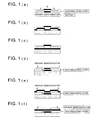
- elements of the invention are arranged as shown in Fig. 1, for example.
- the elements are composed of gate electrode G, gate insulating film I, active layer by an organic semiconductor P, source electrode S and drain electrode D.
- the gate electrode is arranged to be above the organic semiconductor layer on the supporting substrate (hereinafter referred to as "the support” for simplicity)
- Fig. 1(a) represents an example wherein the organic semiconductor layer is arranged between the source electrode and the drain electrode to connect them
- Fig. 1(b) represents an example wherein the organic semiconductor layer is arranged to stretch over the source electrode and the drain electrode to cover them
- Fig. 1(c) represents an example wherein the organic semiconductor layer is arranged to stretch under the source electrode and the drain electrode to connect them.
- Figs. 1(d), 1(e) and 1(f) are an example wherein the organic semiconductor layer is arranged to be above the gate electrode on the support.
- Arrangements of Figs. 1(d), 1(e) and 1(f) in arrangements of the organic semiconductor layer for the source electrode and the drain electrode correspond to the aforesaid arrangements of Figs. 1(a), 1(b) and 1(c)
- Fig. 1(a) represents an example wherein the organic semiconductor layer is arranged between the source electrode and the drain electrode to connect them
- Fig. 1(b) represents an example wherein the organic semiconductor layer is arranged to stretch over the source electrode and the drain electrode to cover them
- Fig. 1(c) represents an example wherein the organic semiconductor layer is arranged to stretch under the source electrode and the drain electrode to connect them.
- ⁇ -conjugated polymers are ⁇ -conjugated polymers.
- employed may be polypyrroles such as polypyrrole, poly(N-substituted pyrrole), poly(3-substituted pyrrole), and poly(3,4-disubstituted pyrrole); polythiophenes such as polythiophene, poly(3-substituted thiophene), poly(3,4-disubstituted thiophene), and polybenzothiophene; polyisothianaphthenes such as polyisothianaphthene; polythienylenevinylenes such as polythienylenevinylene; poly(p-phenylenevinylenes) such as poly(p-phenylenevinylene); polyanilines such as polyaniline, poly(N-substituted aniline), poly(3-substituted aniline), and poly(2,3-substituted aniline); poly
- oligomers having the same repeating units as said polymers such as thiophene hexamers including ⁇ -sexithiophene ⁇ , ⁇ -dihexyl- ⁇ -sexithiophene, ⁇ , ⁇ -dihexyl- ⁇ -quiinquethiophene, ⁇ , ⁇ -bis(3-butoxypropyl)- ⁇ -sexithiophene, and styrylbenzene derivatives.
- metal phthalocyanines such as copper phthalocyanine, and fluorine-substituted copper phthalocyanines, described in Japanese Patent Publication Open to Public Inspection No.
- condensed cyclic tetracarboxylic acid diimides including naphthalenetetracarboxylic acid imides such as 1,4,5,8-teracarboxylic acid diimide, N,N'-bis(4-trifluoromethylbenzyl)naphthalene-1,4,5,8-tretracarboxylic acid diimide, as well as naphthalenetetracarboxylic acid diimides such as N,N'-bis(1H,1H-perfluoroctyl), N,N'-bis(1H,1H-perfluorobutyl) and N,N'-dioctylnaphthalene1,4,5,8-tetracarboxylic acid diimide derivatives, naphthalenetetracarboxylic acid diimides such as naphthalene-2,3,6,7-tetracarboxylic acid diimides; anthracenetetracarbocylic acid diimides such as
- ⁇ conjugated compounds preferably employed is at least one selected from the group consisting of thiophene, vinylene, thienylenevinylene, phenylenevinylene, p-phenylene, substitution products thereof, oligomers which have at least two of these as a repeating unit and have the number n of repeating units of 4 to 10 or polymers which have the number n of said repeating units of at least 20, condensed polycyclic aromatic compounds such as pentacene, fullerenes, condensed cyclic tetracarboxylic acid diimides, and metal phthalocyanines.
- organic molecular complexes such as a tetrathiafulvalene (TTF)-tetracyanoquinodimethane (TCNQ) complex, a bisethylenetetrathiafulvalene (BEDTTTF)-perchloric acid complex, a BEDTTTF-iodine complex, and a TCNQ-iodine complex.
- TTF tetrathiafulvalene
- BEDTTTF bisethylenetetrathiafulvalene
- TCNQ-iodine complex a bisethylenetetrathiafulvalene
- TCNQ-iodine complex a bisethylenetetrathiafulvalene
- employed may be ⁇ conjugated system polymers such as polysilane and polygermane, as well as organic-inorganic composite materials described in Japanese Patent Publication Open to Public Inspection No. 2000-260999.
- the organic semiconductor layer may be subjected to a so-called doping treatment by incorporating in said layer, for example, acrylic acid, acetamide, materials having a functional group such as a dimethylamino group, a cyano group, a carboxyl group and a nitro group, materials such as benzoquinone derivatives, and tetracyanoethylene as well as tetracyanoquinodimethane, and derivatives thereof, which work as an acceptor which accepts electrons, or, for example, materials having a functional group such as an amino group, a triphenyl group, an alkyl group, a hydroxyl group, an alkoxy group, and a phenyl group; substituted amines such as phenylenediamine; anthracene, benzoanthracene, substituted benzoanthracenes, pyrene, substituted pyrene, carbazole and derivatives thereof, and tetrathiafulvalene and derivatives thereof
- the doping means that electron accepting molecules (acceptors) or electron donating molecules (donors) are incorporated in said thin film employing doping.
- the thin film, which has been subjected to said doping is one which comprises said condensed polycyclic aromatic compounds as well as dopants.
- Employed as dopants used in the present invention may be either acceptors or donors.
- donors may be alkaline metals such as Li, Na, K, Rb, and Cs; alkaline earth metals such as Ca, Sr, and Ba; rare earth metals such as Y, La, Ce, Pr, Nd, Sm, Eu, Gd, Tb, Dy, Ho, Er, and Yb; an ammonium ion; R 4 P + , R 4 AS + , and R 3 S + ; and acetylcholine.
- dopants may be carried out employing either a method in which a thin organic semiconductor film is prepared and subsequently, said dopants are incorporated, or a method in which dopants are incorporated during preparation of a thin semiconductor film.
- former methods may be a gas phase doping in which gaseous dopants are employed, and a liquid phase doping in which doping is carried out while said thin film comes into contact with a dopant solution or liquid dopants. Further, in said liquid phase doping, it is possible to adjust the doping efficiency utilizing electrolysis. In the latter methods, either a solution or a dispersion, consisting of organic semiconductors and dopants, may be coated and subsequently dried. For instance, when a vacuum deposition method is used, dopants may be incorporated by achieving codeposition of semiconductor compounds together with dopants.
- dopants may be incorporated in said thin film through sputtering, utilizing the two-dimensional target of said organic semiconductors and said dopants.
- chemical doping such as electrochemical doping or photoinitiation doping, or the physical doping such as an ion injection method shown in, for example, a publication "Kogyo Jairyo (Industrial Materials)", Volume 34, No. 4, page 55 (1986).
- Listed as methods for preparing said thin organic films are a vacuum deposition method, a molecular beam epitaxial growth method, an ion cluster beam method, a low energy ion beam method, an ion plating method, a CVD method, a sputtering method, a plasma polymerization method, an electrolytic polymerization method, a chemical polymerization method, a spray coating method, a spin coating method, a blade coating method, a dip coating method, a casting method, a roll coating method, an bar coating method, a die coating method, and an LB method, which may be employed based on materials.
- a spin coating method, a blade coating method, a dip coating method, a roll coating method, a bar coating method, and a die coating method are preferred which can simply and accurately form a thin film employing an organic semiconductor solution.
- the thickness of the thin film comprised of said organic semiconductors is not particularly limited. However, since the characteristics of the resultant transistors often vary depending on the thickness of the active layer comprised of organic semiconductors, the thickness varies depending on the organic semiconductors, but is commonly at most 1 ⁇ m, and is preferably from 10 to 300 nm.
- Materials for constituting the gate, source, and drain electrodes are not particularly restricted as long as they are electrically conductive materials.
- Employed as materials are platinum, gold, silver, nickel, chromium, copper, iron, tin, antimony, lead, tantalum, indium, palladium, tellurium, rhenium, iridium, aluminum, ruthenium, germanium, molybdenum, tungsten, tin oxide-antimony, indium oxide-tin (ITO), fluorine-doped zinc oxide, zinc, carbon, graphite, glassy carbon, silver paste as well as carbon paste, lithium, beryllium, sodium, magnesium, potassium, calcium, scandium, titanium, manganese, zirconium, gallium, niobium, sodium, sodium-potassium alloy, magnesium, lithium, aluminum magnesium/copper mixtures, magnesium/silver mixtures, magnesium/aluminum mixtures, magnesium/indium mixtures, aluminum/aluminum oxide mixtures, and lithium/alumin
- electrically conductive polymers such as electrically conductive polyaniline, electrically conductive polypyrrole, electrically conductive polythiophene, and complexes of polyethylenedioxythiophene and polystyrnesulfonic acid which increase electrical conductivity upon being doped.
- Methods for forming electrodes include a method in which an electrode is prepared in such a manner that a photolithographic method or a lift-off method, known in the art, is applied to electrically conductive layer, which has been formed employing a vacuum evaporation or sputtering method while employing the aforesaid compounds as a raw material, and a method in which etching is conducted employing a resist which has been prepared employing thermal transfer or ink jet printing onto a foil of metal such as aluminum or copper. Further, an electrically conductive polymer solution or dispersion, or a minute electrically conductive particle dispersion may be subjected directly to patterning, employing ink jet printing.
- Said electrode may also be formed in such a manner that a coated layer is subjected to lithograph or laser ablation.
- a method may also be employed in which ink comprising either an electrically conductive polymer or minute electrically conductive particles, or electrically conductive paste is subjected to patterning, employing any of the printing methods such as letter press, intaglio printing, lithography, or screen printing.
- An electrode which is formed by thermally fusing minute metal particles, having a diameter of 1 to 50 nm, and preferably having a diameter of 1 to 10 nm.
- Employed as metals may be platinum, gold, silver, nickel, chromium, copper, iron, tin, tantalum, indium, cobalt, palladium, tellurium, rhenium, iridium, aluminum, ruthenium, germanium, molybdenum, tungsten, and zinc. Of these, particularly preferred are platinum, gold, silver, copper, cobalt, chromium, iridium, nickel, palladium, molybdenum, and tungsten, which have a work function of at least 4.5 eV.
- minute electrically conductive particles having a diameter of 1 to 50 nm and preferably having from 1 to 10 nm, are minute particles of metals such as platinum, gold, silver, copper, cobalt, chromium, iridium, nickel, palladium, molybdenum, and tungsten.
- metals such as platinum, gold, silver, copper, cobalt, chromium, iridium, nickel, palladium, molybdenum, and tungsten.
- production methods of such minute metal particle suspension are physical preparation methods such as an in-gas evaporation method, a sputtering method, and a metal vapor synthesis method, and chemical preparation methods such as a colloid method and a coprecipitation method in which metal ions are reduced in a liquid phase so that minute metal particles are formed.
- dispersions which are prepared using the colloid methods described in Japanese Patent Publication Open to Public Inspection Nos. 11-76800, 11-80647, 319538, and 2000-239853 and the in-gas evaporation method described in Japanese Patent Publication Open to Public Inspection Nos. 2001-254185, 2001-53028, 2001-35814, 2001-35255, 2000-124157, and 2000-123634.
- solvents are vaporized.
- the resultant is further subjected to a thermal treatment at 100 to 300 °C and preferably at 150 to 200 °C, whereby an electrode is formed by thermally fusing said minute metal particles.
- the gate line as well as the source line may be formed in the same manner as said electrode.
- insulation layers may be employed. Of these, layers, which are comprised of silicon oxide, silicon nitride, aluminum oxide, tantalum oxide, or titanium oxide, are particularly preferred. In the present invention, said insulation layer is specifically formed under an atmospheric pressure, employing a plasma layer forming process.
- a forming method of an insulating film (for example, oxide: SiO 2 , TiO 2 etc. / nitride: Si 3 N 4 etc.) by Plasma film forming processing under the atmospheric pressure is explained as follows.
- the plasma film forming processing under the atmospheric pressure means a processing wherein a reactive gas is plasma-excited by discharge conducted under the atmospheric pressure or the pressure near the atmospheric pressure and a thin film is formed on the elementb material, and its method is described in TOKKAIHEI No. 11-133205, TOKKAI No. 2000-185362, TOKKAIHEI No. 11-61406 and TOKKAI Nos. 2000-147209 and 2000-121804 (hereinafter referred to also as an atmospheric pressure plasma method). Owing to this, it is possible to form thin films with high functions in the high productivity.
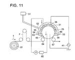
- Fig, 11 is a diagram showing an apparatus conducting plasma film forming processing.
- plasma discharge processing container 31 there are arranged plasma discharge processing container 31, gas generating device 51, power supply 41, and electrode cooling unit 60, as the constitution of the apparatus.
- gas generating device 51 As a cooling agent for the electrode cooling unit 60, insulating materials such as distilled water and oil are used.
- roll electrode 25 and fixed electrode 36 are arranged at prescribed positions, and a mixed gas generated by the gas generating device 51 is controlled in terms of a flow rate to be put in the plasma discharge processing container 31 from air inlet 52, and a mixed gas to be used for plasma processing is filled in the plasma discharge processing container 31, to be exhausted from air outlet 53.
- voltage is impressed on the electrode 36 by power supply 41, and the roll electrode 25 is grounded on the ground to generate discharge plasma.
- base material F is supplied by roll-shaped mater roll base material 61, and base material F wound around the roll electrode 25 through guide roller 64 is pressed by nip rollers 65 and 66 and is conveyed through the gap between both electrodes in the plasma discharge processing container 31 under the state of one-sided contact (contacting roll electrode 25), thus, the surface of the base material F is discharge-processed by discharge plasma, and after that, it is conveyed to the next process through guide roller 67. In this case, the surface of the base material F that does not contact the electrode 25 only is discharge-processed.
- partitioning plate 54 is arranged to be close to the nip rollers 65 and 66, and it controls approach of air that enters the plasma discharge processing container 31.
- Roll electrode 25, serving as a ground electrode is composed of a combination wherein ceramic sealing processed dielectric made by sealing conductive base material such as metal by using inorganic material after injecting melted ceramic. Or, it may also be a combination wherein lining processed dielectric, in which inorganic material is provided on conductive base material by lining, is covered.
- a lining material there are preferably used silicate type glass, borate type glass, phosphate type glass, germanate type glass, tellurite type glass, aluminate type glass and vanadate type glass, and among these, borate type glass is used more preferably because it is easy to be processed.
- a conductive base material such as metal
- metals such as silver, platinum, stainless steel, aluminum and iron, and stainless steel is preferable from the viewpoint of processing.
- a ceramic material used for the melted ceramic injection process alumina, silicon nitride, etc. are preferably used, and among these, alumina is used more preferably because processing is easy.
- base material of roll electrode it is possible to use a base material of jacket roll that made of stainless steel and has a cooling means by cooled water (not shown in the drawings).
- the high frequency power supply made by Pearl Industry (200 kHz), the high frequency power supply made by Pearl Industry (800 kHz), the high frequency power supply made by Nihon Denshi (13.56 MHz) and high frequency power supply made by Pearl Industry (150 MHz), etc. can be employed for this purpose, though there is no limitation for that in particular.
- a distance between the impression electrodes mentioned above is determined by considering a thickness of solid-state dielectric provided on the base material of the electrode, an amplitude of the voltage to be applied, an object for employing plasma, etc.
- a shortest distance between the solid dielectric on the occasion where the solid dielectric is provided on one of the electrodes and the electrode and a distance between solid dielectrics in the case of arranging the solid dielectrics both of the aforesaid electrodes it is preferable that both of them are 0.5 - 20 mm from the viewpoint of conducting even discharging, and especially preferably is 1 mm ⁇ 0.5 mm.
- An upper limit value of the frequency of the high frequency voltage to be applied onto the space between both electrodes is preferably 150 MHz or less.
- a lower limit value of the frequency of the high frequency voltage is preferably 200 kHz or more, and more preferable is 800 kHz or more.
- a lower limit value of power to be supplied between the electrodes is preferably 1.2 W/cm2 or more, and an upper limit value is preferably 50 W/cm2 or less, and more preferable is 20 W/cm2 kHz or less.
- an area (/cm2) for impression of voltage on the electrode means an area of a range where electric discharge occurs.
- a value of voltage to be applied onto electrode 36 fixed by power supply 41 is determined appropriately.
- a continuous mode in the continuous sine wave form that is called a continuous mode
- the intermittent oscillation mode conducting ON/OFF intermittently that is called a pulse mode
- a densely film having excellent quality can be obtained by the continuous mode.
- the temperature of the base material is in the range from ordinary temperature (15°C - 25°C) - 200°C, and the more preferable is to control from ordinary temperature - 100°C.
- discharge plasma processing is conducted while the electrode and the base material are cooled by the cooling means when necessary.
- the discharge plasma processing is conducted under the atmospheric pressure or under the pressure in the vicinity of atmospheric pressure, and the pressure in the vicinity of the atmospheric pressure indicates the pressure of 20 kPa - 110 kPa, and the preferable is 93 kPa - 104 kPa.
- the maximum hight (Rmax) of the surface roughness stipulated by JIS B 0601 is adjusted to be 10 ⁇ m, and more preferable is that the maximum value of the surface roughness is 8 ⁇ m or less, and an especially preferable value is 7 ⁇ m or less.
- gases to be used vary depending on the kind of films provided on the substrate.
- said gas is a mixture consisting of inert gases and reactive gases which are used to form said thin layer.
- the content ratio of said reactive gases is preferably from 0.01 to 10.00 percent by volume of the mixed gas.
- inert gases elements of group 18 of the Periodic Table, specifically including helium, neon, argon, krypton, xenon and radon. Of these, helium as well as argon is preferably employed.
- an electrically conductive layer, an antistatic layer, or the intermediate refractive index layer of a reflection minimizing layer by employing reactive gases comprising at least one organic metal compound selected from the group consisting of zinc acetyl acetate, triethylindium, trimethylindium, diethylzinc, dimethylzinc, tetraethyltin, tetramethyltin, diacetic acid di-n-butyltin, tetrabutyltin, and tetraoctyltin.
- fluorine-containing compounds are fluorine-carbon compounds such as hexafluorinated propylene (CF 3 CFCF 2 ) and octafluorinated butane (C 4 F 8 ). From the viewpoint of safety, are employed hexafluorinated propylene and octafluorinated butane which do not from hazardous hydrogen fluoride gas.
- hydrophilic polymerization layer by carrying out a treatment under an atmosphere of monomers having a hydrophilic group as well as polymerizable unsaturated bonds in the molecules.
- hydrophilic groups are a hydroxyl group, a sulfonic acid group, a sulfonic acid salt group, a primary, secondary, or tertiary amino group, an amido group, a quaternary ammonium salt group, a carboxylic acid group, and a carboxylic acid salt group. It is also possible to accumulate said hydrophilic polymerization layer in the same manner as above by using monomers having polyethylene glycol chains.
- Listed as said monomers are acrylic acid, methacrylic acid, acrylamide, methacrylamide, N,N-dimethylacrylamide, sodium acrylate, sodium methacrylate, potassium acrylate, potassium methacrylate, sodium styrenesulfonate, allylalcohol, allylamine, polyethylene glycol dimethacrylic acid esters, and polyethylene glycol diacrylic acid esters. It is possible to use at least one of these.
- fluorinated carbon gases Preferably employed as organic fluorine compounds are fluorinated carbon gases and fluorinated hydrocarbon gases.
- fluorinated carbon gases are tetrafluorinated carbon and hexafluorinated carbon, specifically including tetrafluorinated methane, tetrafluorinated ethylene, hexafluorinated propylene, and octafluorinated cyclobutane.
- halides of fluorinated hydrocarbons such as monochlorinated trifluorinated methane, monochlorinated difluorinated methane, and dichlorinated teterafluorinated butane, and fluorine substitution compounds of alcohols, acids and ketones.
- fluorinated hydrocarbons such as monochlorinated trifluorinated methane, monochlorinated difluorinated methane, and dichlorinated teterafluorinated butane
- fluorine substitution compounds of alcohols, acids and ketones such as monochlorinated trifluorinated methane, monochlorinated difluorinated methane, and dichlorinated teterafluorinated butane
- these compounds may have ethylenic unsaturated bonds in the molecules. Said compounds may be employed individually or in combination.
- the content ratio of said organic fluorine compounds in said mixed gases is preferably from 0.1 to 10.0 percent by volume, and is more preferably from 0.1 to 5.0 percent by volume.
- organic fluorine compounds when said organic fluorine compounds are in the form of gas at normal temperature and normal pressure, they may be employed as a component of said mixed gas without any modification. As a result, they may be readily employed.
- organic fluorine compounds when said organic fluorine compounds are in the form of liquid or solid at normal temperature and normal pressure, they may be employed upon being gasified employing methods such as heating and pressure reduction. Further, they may be employed upon being dissolved in suitable solvents.
- the content ratio of said titanium compounds in said mixed gases is preferably from 0.1 to 10.0 percent by volume, and is more preferably from 0.1 to 5.0 percent by volume.
- metal hydrogen compounds and metal alkoxides are more preferably employed, since they are not corrosive, do not generate hazardous gases and result in minimal staining during processing.
- silicon compounds as well as titanium compounds into the space between electrodes, which is employed as a discharge space, may be carried out irrespective of their states such as gas, liquid, or solid.
- they are in the form of gas it is possible to introduce into said discharge space without any modification.
- they are in the form of liquid or solid they are used upon being gasified employing methods such as heating, pressure reduction, and ultrasonic wave application.
- metal alkoxides are suitably employed which are in the form of liquid at normal temperature, having a boiling pint of less than or equal to 200 °C.
- Said metal alkoxides may be employed upon being diluted by solvents.
- Employed as said solvents may be organic solvents such as methanol, ethanol, and n-hexane, and mixtures thereof.
- organic solvents such as methanol, ethanol, and n-hexane, and mixtures thereof.
- silicon compounds Preferably employed as said silicon compounds are, for example, organic metal compounds such as dimethylsilane and tetramethylsilane, metal hydrogen compounds such as monosilane and disilane, metal halogen compounds such as dichlorinated silane and trichlorinated silane, alkoxysilanes such as tetramethoxysilane, tetraethoxysilane, and dimethylethoxysilane, and organosilanes.
- organic metal compounds such as dimethylsilane and tetramethylsilane
- metal hydrogen compounds such as monosilane and disilane
- metal halogen compounds such as dichlorinated silane and trichlorinated silane
- alkoxysilanes such as tetramethoxysilane, tetraethoxysilane, and dimethylethoxysilane
- organosilanes organosilanes.
- the present invention is not limited to these. Further, these may be
- the content ratio of said silicon compounds in said mixed gases is preferably from 0.1 to 10.0 percent by volume, and is more preferably from 0.1 to 5.0 percent by volume.
- titanium compounds Preferably employed as said titanium compounds are organic metal compounds such as tetradimethylaminotitanium, metal hydrogen compounds such as monotitanium and dititanium, metal halogen compounds such as titanium dichloride, titanium trichloride, and titanium tetrachloride, and metal alkoxides such as tetraethoxytitanium, tertaisopropoxytitanium, tetrabutoxytitanium.
- organic metal compounds such as tetradimethylaminotitanium, metal hydrogen compounds such as monotitanium and dititanium, metal halogen compounds such as titanium dichloride, titanium trichloride, and titanium tetrachloride, and metal alkoxides such as tetraethoxytitanium, tertaisopropoxytitanium, tetrabutoxytitanium.
- metal hydrogen compounds such as monotitanium and dititanium
- metal halogen compounds
- Plastic films may be employed as a sheet.
- plastic films are those which are comprised of, for example, polyethylene terephthalate (PET), polyethylene naphthalate (PEN), polyethersulfone (PES), polyetherimide, polyetherketone, polyphenylenesulfide, polyallylate, polyimide, polycarbonate (PC), cellulose triacetate (TAC), and cellulose acetate propionate (CAP).
- PET polyethylene terephthalate
- PEN polyethylene naphthalate
- PES polyethersulfone
- PES polyetherimide
- polyetherketone polyphenylenesulfide
- polyallylate polyimide
- PC polycarbonate
- TAC cellulose triacetate
- CAP cellulose acetate propionate
- a vacuum evaporation film formed by employing silicon oxide together with aluminum oxide, a film comprised of metal oxides such as silicon oxide and aluminum oxide, which is prepared employing an atmospheric pressure plasma method, or a multilayered composite film may be formed as a gas barrier layer.
- a composite film may be employed which is prepared by laminating films vacuum-deposited with a thin layer comprised of metals such as aluminum, or minute metal oxide particles may be incorporated in said film.
- said organic semiconductor layer is separated from atmosphere by the use of a protective film.
- gas barrier films comprised of PVA and ethylenevinyl alcohol copolymers, and metal oxides and metal nitrides, known in the art.
- metal oxides and metal nitrides may be silicon oxide, aluminum oxide, tantalum oxide, titanium oxide, silicon nitride, and aluminum nitride.
- methods for forming said protective film are those using dry processes such as a vacuum deposition method, a molecular beam epitaxial growth method, an ion cluster beam method, a low energy ion beam method, an ion plating method, a CVD method, a sputtering method, and an atmospheric pressure plasma method, and wet processes using coating methods such as a spray coating method, a spin coating method, a blade coating method, a dip coating method, a casting method, a roll coating method, an bar coating method, as well as methods employing patterning such as printing and ink jet printing. It is possible to employ any of these methods based on materials. Of these, the aforesaid atmospheric pressure plasma method is preferred.
- the thickness of these insulation films is commonly from 50 nm to 3 ⁇ m, and is preferably from 100 nm to 1 ⁇ m.
- Fig. 2 is a block diagram showing the overall structure of the display panel.
- Each pixel arranged in a matrix form on display panel 100 of display device has a flat plate electrode 1 (display image section in the drawing) that accumulates electric charges and gives an electric field to a liquid crystal.
- a transistor section (TFT drive section 2) that switches ON and OFF of the electric current to the flat plate electrode and capacitor 3 are arranged for each flat plate electrode.
- the capacitor 3 accumulates electric charges and keeps them at the prescribed timing to maintain the electric field for the corresponding flat plate electrode 1.
- Driving control of liquid crystal by these flat plate electrodes is executed by the aforesaid TFT driving section 2, and this is controlled by power supply line (source line 4) corresponding to the pixel controlled by vertical drive circuit 6 and by control signal line (gate line 5) corresponding to the pixel controlled by horizontal drive circuit 7.
- Memory 9 is a buffer memory for holding image data for one image plane, for example, and the control circuit 8 reads required image signals from the memory 9.
- display material 11 such as liquid crystal is sealed to be sandwiched by the flat plate electrode 1 and surface electrode 10 arranged above the flat plate electrode 1.
- organic EL and an element using electrophoresis in addition to liquid crystal can be used. Then, electric field is applied on display material 11 of display pixel section, responding to the control of the TFT driving section 2, and display is controlled at a unit of pixel.
- the aforementioned surface electrode 10 has light transmission property, and a transparent conductive film is used as a practical example.
- the transparent conductive film is formed by using conductive transparent material such as, for example, indiumtinoxide (ITO),SnO2, or ZnO.
- ITO indiumtinoxide
- a thin film can be formed by employing a method of evaporation deposition or a method of sputtering. It is preferable for the transparent conductive film that its transmission factor is greater than 10%, and sheet resistance is several hundreds ⁇ /sq. or less.
- Coating thickness is formed to be a thickness of 10 nm or more, though it depends a material. The reason for the foregoing is that when the coating thickness is thin, transparent electrodes become a shape of islands.
- the transparent conductive film can be applied of forming of the flat plate electrode 1, and in this case, a desired form pattern may be formed through a photolithography method, or a pattern may be formed through a desired form mask in the case of evaporation deposition or sputtering of the aforesaid electrode substances.
- the prescribed transparent protective layer on the upper position of the surface electrode 10, and for example, it is possible to form the functional film such as a reflection prevention layer.
- S represents a source electrode
- D represents a drain electrode
- G means a gate electrode
- S, D and G constitute TFT driving section 2.
- Cs represents a capacitor for holding an electric field to be applied onto liquid crystal or other display medium.
- source voltage Vs is applied onto the source electrode S
- gate voltage Vg is applied onto the gate electrode G.
- Fig. 5 mostly corresponds to a sectional view on line X in Fig. 2.
- Each of said plate electrodes (1, 1', and 1") is arranged on first support 12 at even intervals.
- Said first support 12 is comprised of a flexible resinous sheet.
- a plastic film as said sheet.
- films comprised of, for examples, polyethylene terephthalate (PET), polyethylene naphthalate (PEN), polyethersulfone (PES), polyetherimide, polyether ether ketone, polyphenylenesulfide, polyallylate, polyimide, polycarbonate (PC), cellulose triacetate (TAC), and cellulose acetate propionate (CAP).
- PET polyethylene terephthalate
- PEN polyethylene naphthalate
- PES polyethersulfone
- PES polyetherimide
- polyether ether ketone polyphenylenesulfide
- PC polycarbonate
- TAC cellulose triacetate
- CAP cellulose acetate propionate
- plasticizers such as trioctyl phosphate and dibutyl phthalate may be incorporated in these plastic films and benzotriazole based or benzophenone based UV absorbers, known in the art, may also be incorporated in the same.
- Each flat plate electrode (1, 1', 1") and each source line (4, 4', 4") are arranged side by side while keeping the prescribed interval. Then, organic semiconductor section (13, 13', 13") are arrange to bridge flat plate electrode ends and corresponding source lines (4, 4', 4") (the same as Fig. 1 (a) and 1 (b)).
- an insulating layer 14 (insulating film).
- insulating film of SiO 2 or TiO 2 can be used.
- the insulating layers 14 are formed at the positions to insulate source for a current path from the source lines (4, 4', 4") to the flat plate electrodes (1, 1', 1") on the pattern of the organic semiconductor section (13, 13', 13") and for the gate line 5 to be arranged in the next step.
- insulating layers 14 When forming insulating layers 14 in the aforesaid method, on the entire surface of the first support 12, it is not necessary to control the positions of formation of insulating layers depending on the organic semiconductor section (13, 13', 13") or the intersecting sections between gate line 5 and source lines (4, 4', 4"). Further, because of the improvement of the line speed in manufacturing process, an insulating layer can be formed in a short time even a panel is large in area.
- insulating layer 14 for each pixel for the organic semiconductor section (13, 13', 13") or the intersecting sections between gate line 5 and source lines (4, 4', 4").
- An ink jet method can be used as a forming method.
- insulating film 14 can be coated broadly to cover both the organic semiconductor section (13, 13', 13") and the intersecting sections between gate line 5 and source lines (4, 4', 4"). In this case, it is possible to reduce raw material cost by securing switching operations even for patterning with low accuracy though processing speed is restricted, rather than making insulating film on the entire surface of the support.
- insulating layer 14 When providing insulating layer 14 on the entire surface of the first support 12, or when providing partially, in any case, if the same insulating layer 14 covers the organic semiconductor section (13, 13', 13") and the intersecting sections between gate line 5 and source lines (4, 4', 4"), it is possible to simplify the forming process of insulating layers.
- the gate line 5 intersects with the source lines (4, 4', 4") at right angles, and is arranged to be positioned above the organic semiconductor section (13, 13', 13") (described later, referring to Fig. 7).
- the second support is arranged above the gate line 5 of the corresponding pixel through display material 11 (liquid crystal, etc.).
- This second support has conductivity and it becomes a facing electrode for the flat plate electrodes (1, 1', 1") of each pixel.
- the conductive film 10 transparent conductive film is preferable
- This conductive film 10 can be provided at least the position corresponding to the flat plate electrodes (1, 1', 1") of each pixel, and it is possible to make facing electrode easily by covering the entire surface of the second support with conductive film and by grounding them.
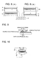
- the conductive thin-layer 16 mentioned above is grounded (refer to Fig. 6(B)).
- the conductive thin-layer 16 is formed on the entire surface of the first support 12 in the above example, by arranging a plurality of conductive earth-lines so as to face the flat electrode 1, it is also possible to form a capacitor structure between the plurality of conductive earth-lines and the flat electrode 1. In this case, the plurality of conductive earth-lines are grounded as well as the conductive thin-layer 16 mentioned above.
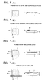
- Figs. 7(A) - 7(D) show a schematic diagram of a formation process of materials onto the first support 12. In the following, the formation process with respect to one pixel will be detailed.
- a plurality of source lines and a plurality of flat electrodes are formed on the first support 12 in advance (refer to Fig. 7(A)).
- the spattering method is employed for forming source lines 4 and flat electrodes 1 in the this example.
- a solution or a dispersed-liquid of the organic semiconductor material is employed for the patterning process, so that the organic material dispersed-liquid overlaps both each of source lines 4 and each of flat electrodes 1 (refer to Fig. 7(B)). Since the organic material dispersed-liquid, employed for the patterning process, exhibits a high fluidity, the dot formation by means of the ink-jetting method is employed for the patterning process. Pattern 13 of the organic semiconductor material could be an arbitral shape, though pattern 13 is conceptually illustrated. Of cause, this patterning process also can be achieved by application and drying process after the masking process, for which conventional well-known methods, such as the electro-photographic method, etc., can be employed. According to the abovementioned patterning method, it becomes possible to form the semiconductor layer in an environment of normal pressure without repeating vapor-depositing processes and etching processes as performed in the conventional Si-semiconductor process.
- the organic semiconductor section 13, formed by the abovementioned process, is arranged so as to connect a part of flat electrodes 1 with source line 4.
- the organic semiconductor is formed as a dot so as to cover both an end portion of flat electrode 1 and a part of source line 4.
- a part of flat electrode 1 is continuously coupled to source line 4 only by a single semiconductor material.
- an arbitral electrode is inserted between the organic semiconductor section 13 and the flat electrode 1 or between the organic semiconductor section 13 and the source line 4, in order to support the electronic connection.
- the insulating layer 14 of SiO 2 is formed on the pattern of the abovementioned organic semiconductor section 13, formed in the process shown in Fig. 7(B), (refer to Fig. 7(C).
- the insulating layer 14 covers the entire surface of the panel 100, and also covers both the electronic current path from the source line 4 to the flat electrode 1 on the organic semiconductor pattern and a position at which the source line 4 is insulated from the gate line 5 to be arranged in the next process (a position at which the source line 4 and the gate line 5 crosses each other).
- the insulating layer 14 mentioned above is formed by the plasma film formation processing under the atmospheric pressure, and by employing the mixed gas for forming the SiO 2 layer. Since the insulating layer 14 is formed over the entire surface of the first support 12 as aforementioned, it is not necessary to control the forming position of the insulating layer 14 in response to the intersecting position of gate line 5 and source line 4. Since the processing can be performed under the atmospheric pressure, it becomes possible to introduce the conveyer method into the manufacturing line, and therefore, it becomes possible to shorten the formation time for the insulating layer 14 by improving the conveyer speed of the manufacturing line, even if the large-sized panel is manufactured in the line.
- the gate line 5 is formed on the insulating layer 14 in such a manner that the gate line 5 crosses the source line 4 (in this example, the gate line 5 is orthogonal to the source line 4) and covers the organic semiconductor section 13.
- This pattern can be formed by the method of applying or transferring the conductive material, or by the method of continuously forming ink-jetting dots.
- the gate line 5 is a signal line, which also works as a gate electrode crossing the organic semiconductor section 13 and directly affecting to the organic semiconductor section 13 as it is without diverging.
- the insulating layer 14 is made of SiO 2 in the abovementioned patterning process
- TiO 2 also can be employed for forming the insulating layer 14 (in the process shown in Fig. 7(C)).
- the insulating layer 14 is formed by the plasma film formation processing under the atmospheric pressure, and by employing the mixed gas for forming the TiO 2 layer.
- the structure other than the abovementioned insulating layer 14 is the same as that in the foregoing.
- the insulating layer 14 made of TiO 2 covers the entire surface of the panel 100, and also covers both the electronic current path from the source line 4 to the flat electrode 1 on the organic semiconductor pattern and a position at which the source line 4 is insulated from the gate line 5 to be arranged in the next process (a position at which the source line 4 and the gate line 5 crosses each other).
- the opposing electrode is formed on the second support, and conductivity is added to the surface of the opposing electrode.
- the conductive thin-layer 16 is formed at at-least a position facing to the plurality of flat electrodes on the first support 12.
- a transparent conductive thin-layer 16 is formed over the entire surface of the second support.
- the display material 11 is injected into the space, maintaining a predetermined gap, between the third support and the second support, and is sealed in it. While, in the latter case, the display material 11 is injected into the space, maintaining a predetermined gap, between the first support 12 and the second support, and is sealed in it.
- the composition of the mixed gas (being the reactive gas), which is employed for the plasma process, will now be described below.
- the atmospheric pressure plasma process is continuously carried out onto the hard coat layer of substrate film 8 under said discharge conditions employing said reactive gases, whereby a 100 nm thin film is provided.
- Discharge output should be set at 10 W/cm 2 .
- a roll electrode comprising a dielectric (having a relative dielectric constant of 10), which is grounded, is prepared as follows.
- a mother stainless steel jacket roll, having a cooling means employing cooling water, is covered with 1 mm thick alumina, employing ceramic spraying.
- a solution prepared by diluting tetramethoxysilane with ethyl acetate is applied and subsequently dried.
- the resultant coating is hardened while exposed to ultraviolet rays so that pores are sealed.
- the resultant surface is then smoothed so as to be Rma x 5 ⁇ m.
- an applied electrode is prepared by covering a hollow square-shaped stainless steel pipe with the same dielectric as above under the same conditions.
- the organic thin film transistor element shown in Fig. 1(a), was prepared as described below.
- a thin 500 ⁇ thick Au film was vacuum-deposited on a 150 ⁇ m thick polyimide film, and each of a source electrode and a drain electrode was formed employing a photolithographic method.
- the channel length was determined to be 20 ⁇ m.
- a chloroform solution of regioregular-poly (3-hexylthiophene), purified as desired, was ejected employing piezoelectric system ink jet and the portion between said source electrode and said drain electrode was filled with said solution. By removing chloroform as a solvent through drying, the resultant was heated at 100 °C for 5 minutes and was set aside at vacuum for 24 hours.
- the resultant thickness of said regioregular-poly (3-hexylthiophene) film was approximately 50 nm.
- a 200 nm thick silicon oxide film was formed on said source electrode, said drain electrode, and said regioregular-poly (3-hexylthiphene), employing the aforesaid atmospheric pressure plasma method.
- a 30 ⁇ m wide gate electrode was formed by employing an Ag paste available in the conventional market, and as a result, the organic thin-film transistor element, shown in the structural example A, is obtained.
- Example A An element was prepared in the same manner as Example A, except that the silicon oxide film was formed employing a conventional sputtering method.
- the leak electric current refers to the leak current value at the gate insulation layer when the voltage between the source and the gate is -30 V
- the breakdown voltage refers to a voltage value at which dielectric breakdown of the gate insulation layer occurs
- the on/off ratio refers to the electric current ratio when the gate voltage is set at -30 V and +30 V, while setting the voltage between the source and the drain at -30 V.
- Leak Electric Current Breakdown Voltage On/Off Ratio Example 1 -0.2 nA -150 V 10000 Comp.
- the organic thin-film transistor element of Example 2 is made and evaluated in the entirely same process as that of Example 1, except that the silicon oxide film of the gate insulation layer is change to the titanium oxide, thickness of which is 200 nm.
- the thin organic film transistor element shown in Fig. 1(b), was prepared as described below.
- a vacuum-deposited Al film was formed on a 150 ⁇ m thick PET film, and subsequently, a 30 ⁇ wide gate electrode was formed employing a photolithographic method.
- a 200 nm thick silicon oxide film was formed on the resultant gate electrode in the same manner as Example 1.
- a thin 300 ⁇ thick Cr film and a thin 500 ⁇ thick Au film were vacuum-deposited one by one, and each of a source electrode and a drain electrode was formed employing a photolithographic method.
- the channel length was determined to be 20 ⁇ m.
- a chloroform solution of regioregular-poly (3-hexylthiophene), purified as desired, was ejected employing piezoelectric system ink jet and the portion between said source electrode and said drain electrode was filled with said solution.
- chloroform as a solvent through drying, the resultant was heated at 100 °C for 5 minutes and was set aside at vacuum for 24 hours.
- the resultant thickness of said regioregular-poly (3-hexylthiophene) film was approximately 100 nm.
- the transistor element was sealed by forming a silicon oxide film having 500 nm thickness through the deposition process. Then, the transistor characteristics were measured in the same process as that of Example 1.
- An element was prepared in the same manner as Example 3, except that a silicon oxide film was formed employing a conventional sputtering method.
- the leak electric current refers to the leak current value at the gate insulation layer when the voltage between the source and the gate is -30 V
- the breakdown voltage refers to a voltage value at which dielectric breakdown of the gate insulation layer occurs
- the on/off ratio refers to the electric current ratio when the gate voltage is set at -30 V and +30 V, while setting the voltage between the source and the drain at -30 V.
- Leak Electric Current Breakdown Voltage On/Off Ratio Example 3 -0.3 nA -140 V 20000 Comp.
- the organic thin-film transistor element of Example 4 is made and evaluated in the entirely same process as that of Example 1, except that the silicon oxide film of the gate insulation layer is change to the titanium oxide, thickness of which is 200 nm.
- the insulation film, formed in the atmospheric pressure plasma method is close and has little defects and exhibits a good electronic-field effect. Accordingly, it becomes possible to reduce the leak current of the gate insulation layer and the gate voltage, and to improve the on/off ratio, resulting in realization of the good performances of the thin-film transistor and improvement of the insulation durability.
- the new combination of the insulation film, formed in the atmospheric pressure plasma method, and the organic semiconductor material exhibits superior effects, compared to the combination of the conventional insulation film and the organic semiconductor material. Since the film formation under the atmospheric pressure environment is possible, the present invention is suitable for processing the flexible base, such as polymer support member, etc., and it is possible to drastically reduce the manufacturing cost of the organic FET.
- the present invention it is possible to improve the characteristics of the device, such as the on/off ratio, the leak current, etc., when the organic semiconductor is employed as the active semiconductor layer in the thin-film TFT of the device. Further, since the formation process of the insulation film does not require a vacuum processing, it becomes possible to reduce the manufacturing cost and to simplify the manufacturing process, resulting in the drastic reduction of the total manufacturing cost.
Landscapes
- Chemical & Material Sciences (AREA)
- Engineering & Computer Science (AREA)
- General Chemical & Material Sciences (AREA)
- Chemical Kinetics & Catalysis (AREA)
- Materials Engineering (AREA)
- Mechanical Engineering (AREA)
- Metallurgy (AREA)
- Organic Chemistry (AREA)
- Physics & Mathematics (AREA)
- Plasma & Fusion (AREA)
- Thin Film Transistor (AREA)
Applications Claiming Priority (2)
| Application Number | Priority Date | Filing Date | Title |
|---|---|---|---|
| JP2001269082 | 2001-09-05 | ||
| JP2001269082 | 2001-09-05 |
Publications (2)
| Publication Number | Publication Date |
|---|---|
| EP1291932A2 true EP1291932A2 (fr) | 2003-03-12 |
| EP1291932A3 EP1291932A3 (fr) | 2006-10-18 |
Family
ID=19094961
Family Applications (1)
| Application Number | Title | Priority Date | Filing Date |
|---|---|---|---|
| EP02019125A Withdrawn EP1291932A3 (fr) | 2001-09-05 | 2002-08-29 | Dispositif semiconductur organique et sa procédé de fabrication |
Country Status (2)
| Country | Link |
|---|---|
| US (2) | US6794220B2 (fr) |
| EP (1) | EP1291932A3 (fr) |
Cited By (13)
| Publication number | Priority date | Publication date | Assignee | Title |
|---|---|---|---|---|
| WO2005010995A1 (fr) * | 2003-07-25 | 2005-02-03 | Fuji Xerox Co., Ltd. | Element electronique, circuit integre et procede de fabrication correspondant |
| WO2005024972A3 (fr) * | 2003-09-03 | 2006-08-24 | Univ Ilmenau Tech | Procede pour produire des composants electroniques |
| EP1361619A3 (fr) * | 2002-05-09 | 2007-08-15 | Konica Corporation | Transistor à couche mince organique, substrat de transistor à couche mince organique, et sa méthode de fabrication |
| EP1732115A4 (fr) * | 2004-03-31 | 2009-03-04 | Konica Minolta Holdings Inc | Feuille tft et méthode de production de celle-ci |
| US7733315B2 (en) | 2004-12-06 | 2010-06-08 | Semiconductor Energy Laboratory Co., Ltd. | Display device |
| CN104167429A (zh) * | 2014-08-01 | 2014-11-26 | 京东方科技集团股份有限公司 | 一种柔性显示面板及其制备方法、显示装置 |
| CN104218152A (zh) * | 2014-09-01 | 2014-12-17 | 南京邮电大学 | 一种有机薄膜晶体管的制备方法 |
| US9786807B2 (en) | 2011-04-19 | 2017-10-10 | Empa | Thin-film photovoltaic device and fabrication method |
| US9837565B2 (en) | 2012-12-21 | 2017-12-05 | Flison Ag | Fabricating thin-film optoelectronic devices with added potassium |
| US10109761B2 (en) | 2014-05-23 | 2018-10-23 | Flisom Ag | Fabricating thin-film optoelectronic devices with modified surface |
| US10396218B2 (en) | 2014-09-18 | 2019-08-27 | Flisom Ag | Self-assembly pattering for fabricating thin-film devices |
| US10651324B2 (en) | 2016-02-11 | 2020-05-12 | Flisom Ag | Self-assembly patterning for fabricating thin-film devices |
| US10658532B2 (en) | 2016-02-11 | 2020-05-19 | Flisom Ag | Fabricating thin-film optoelectronic devices with added rubidium and/or cesium |
Families Citing this family (94)
| Publication number | Priority date | Publication date | Assignee | Title |
|---|---|---|---|---|
| EP1278234B1 (fr) * | 2001-07-19 | 2012-01-11 | STMicroelectronics Srl | Transistor MOS et sa méthode de fabrication |
| KR20020025918A (ko) * | 2002-02-15 | 2002-04-04 | 박병주 | 습식 공정으로 제작된 유기 반도체 디바이스 및 유기전계발광 소자 |
| JP3962862B2 (ja) * | 2002-02-27 | 2007-08-22 | 日立造船株式会社 | カーボンナノチューブを用いた導電性材料およびその製造方法 |
| US7285440B2 (en) * | 2002-11-25 | 2007-10-23 | International Business Machines Corporation | Organic underlayers that improve the performance of organic semiconductors |
| US7078261B2 (en) * | 2002-12-16 | 2006-07-18 | The Regents Of The University Of California | Increased mobility from organic semiconducting polymers field-effect transistors |
| KR100572926B1 (ko) * | 2002-12-26 | 2006-04-24 | 삼성전자주식회사 | 폴리티에닐티아졸 유도체 및 이를 이용한 유기박막트랜지스터 |
| US7183146B2 (en) * | 2003-01-17 | 2007-02-27 | Semiconductor Energy Laboratory Co., Ltd. | Method of manufacturing semiconductor device |
| US7405033B2 (en) * | 2003-01-17 | 2008-07-29 | Semiconductor Energy Laboratory Co., Ltd. | Method for manufacturing resist pattern and method for manufacturing semiconductor device |
| US20060243965A1 (en) * | 2003-01-28 | 2006-11-02 | De Leeuw Dagobert M | Electronic device |
| WO2004075279A1 (fr) * | 2003-02-18 | 2004-09-02 | Konica Minolta Holdings, Inc. | Dispositif de transistor a film mince organique et son procede de fabrication |
| KR100947702B1 (ko) * | 2003-02-26 | 2010-03-16 | 삼성전자주식회사 | 경화성 작용기로 표면수식된 탄소나노튜브를 이용한패턴박막 형성방법 및 고분자 복합체의 제조방법 |
| KR101151096B1 (ko) * | 2006-11-30 | 2012-06-01 | 삼성전자주식회사 | 표면 수식된 탄소나노튜브를 이용한 유기박막 트랜지스터 |
| JP3669363B2 (ja) * | 2003-03-06 | 2005-07-06 | ソニー株式会社 | エレクトロデポジション型表示パネルの製造方法、並びにエレクトロデポジション型表示パネルおよびエレクトロデポジション型表示装置 |
| US6828583B2 (en) * | 2003-03-12 | 2004-12-07 | The Regents Of The University Of California | Injection lasers fabricated from semiconducting polymers |
| US7037767B2 (en) * | 2003-03-24 | 2006-05-02 | Konica Minolta Holdings, Inc. | Thin-film transistor, thin-film transistor sheet and their manufacturing method |
| CN100552893C (zh) * | 2003-03-26 | 2009-10-21 | 株式会社半导体能源研究所 | 半导体装置及其制造方法 |
| US20060261329A1 (en) * | 2004-03-24 | 2006-11-23 | Michele Muccini | Organic electroluminescence devices |
| CN1768437A (zh) * | 2003-03-31 | 2006-05-03 | 佳能株式会社 | 有机薄膜晶体管及其制作方法 |
| WO2004090847A1 (fr) * | 2003-04-02 | 2004-10-21 | Matsushita Electric Industrial Co. Ltd. | Ecran |
| US7192859B2 (en) * | 2003-05-16 | 2007-03-20 | Semiconductor Energy Laboratory Co., Ltd. | Method of manufacturing semiconductor device and display device |
| JP2007516347A (ja) * | 2003-05-16 | 2007-06-21 | イー・アイ・デュポン・ドウ・ヌムール・アンド・カンパニー | 原子層蒸着によって製造されたプラスチック基板用のバリアフィルム |
| KR100503421B1 (ko) * | 2003-05-20 | 2005-07-22 | 한국전자통신연구원 | 채널 재료로서 절연체-반도체 상전이 물질막을 이용한전계 효과 트랜지스터 및 그 제조 방법 |
| DE10324533A1 (de) * | 2003-05-28 | 2004-12-16 | H.C. Starck Gmbh | Stabile Lösungen von organischen halbleitenden Verbindungen |
| CN1574214A (zh) * | 2003-06-03 | 2005-02-02 | 国际商业机器公司 | 用于制造电子器件的基于熔化的图案化工艺 |
| US6927108B2 (en) * | 2003-07-09 | 2005-08-09 | Hewlett-Packard Development Company, L.P. | Solution-processed thin film transistor formation method |
| CN100533770C (zh) * | 2003-07-17 | 2009-08-26 | 松下电器产业株式会社 | 场效应型晶体管及其制造方法 |
| WO2005008787A1 (fr) * | 2003-07-18 | 2005-01-27 | Japan Science And Technology Agency | Capteur optique |
| JP2005063725A (ja) * | 2003-08-08 | 2005-03-10 | Fujitsu Hitachi Plasma Display Ltd | フラットパネルディスプレイの製造方法 |
| DE10340608A1 (de) * | 2003-08-29 | 2005-03-24 | Infineon Technologies Ag | Polymerformulierung und Verfahren zur Herstellung einer Dielektrikumsschicht |
| JP2005093921A (ja) * | 2003-09-19 | 2005-04-07 | Canon Inc | 電界効果型有機トランジスタおよびその製造方法 |
| WO2005041280A1 (fr) | 2003-10-28 | 2005-05-06 | Semiconductor Energy Laboratory Co., Ltd. | Procede de fabrication d'un dispositif a semiconducteur |
| US20050253137A1 (en) * | 2003-11-20 | 2005-11-17 | President And Fellows Of Harvard College | Nanoscale arrays, robust nanostructures, and related devices |
| JP4850389B2 (ja) * | 2003-12-12 | 2012-01-11 | 独立行政法人産業技術総合研究所 | ドーピング方法およびそれを用いた半導体素子 |
| TWI236173B (en) * | 2004-02-13 | 2005-07-11 | Ind Tech Res Inst | Manufacturing method and device for organic thin film transistor |
| TWI228833B (en) * | 2004-05-04 | 2005-03-01 | Ind Tech Res Inst | Method for enhancing the electrical characteristics of organic electronic devices |
| US7704414B2 (en) * | 2004-05-07 | 2010-04-27 | Canon Kabushiki Kaisha | Image-forming method employing a composition |
| US7372070B2 (en) * | 2004-05-12 | 2008-05-13 | Matsushita Electric Industrial Co., Ltd. | Organic field effect transistor and method of manufacturing the same |
| US7456424B2 (en) * | 2004-12-14 | 2008-11-25 | Xerox Corporation | Thin film transistors including indolocarbozoles |
| US7494923B2 (en) | 2004-06-14 | 2009-02-24 | Semiconductor Energy Laboratory Co., Ltd. | Manufacturing method of wiring substrate and semiconductor device |
| US7135405B2 (en) * | 2004-08-04 | 2006-11-14 | Hewlett-Packard Development Company, L.P. | Method to form an interconnect |
| US20060030149A1 (en) * | 2004-08-06 | 2006-02-09 | Steven Leith | Depositing material on photosensitive material |
| KR100615237B1 (ko) * | 2004-08-07 | 2006-08-25 | 삼성에스디아이 주식회사 | 박막 트랜지스터 및 그의 제조방법 |
| JP4616596B2 (ja) * | 2004-08-27 | 2011-01-19 | 株式会社 日立ディスプレイズ | 電子装置の製造方法 |
| JP4341529B2 (ja) * | 2004-11-05 | 2009-10-07 | セイコーエプソン株式会社 | 電子デバイス、電子デバイスの製造方法および電子機器 |
| US7582534B2 (en) * | 2004-11-18 | 2009-09-01 | International Business Machines Corporation | Chemical doping of nano-components |
| US20060125009A1 (en) * | 2004-12-14 | 2006-06-15 | Xerox Corporation | Thin film transistors including indolocarbazoles |
| KR100670255B1 (ko) * | 2004-12-23 | 2007-01-16 | 삼성에스디아이 주식회사 | 박막 트랜지스터, 이를 구비한 평판표시장치, 상기 박막트랜지스터의 제조방법, 및 상기 평판 표시장치의 제조방법 |
| TWI273329B (en) | 2004-12-29 | 2007-02-11 | Au Optronics Corp | Copper gate electrode of liquid crystal display device and method of fabricating the same |
| JP2006269599A (ja) * | 2005-03-23 | 2006-10-05 | Sony Corp | パターン形成方法、有機電界効果型トランジスタの製造方法、及び、フレキシブルプリント回路板の製造方法 |
| US7926726B2 (en) * | 2005-03-28 | 2011-04-19 | Semiconductor Energy Laboratory Co., Ltd. | Survey method and survey system |
| KR100647693B1 (ko) * | 2005-05-24 | 2006-11-23 | 삼성에스디아이 주식회사 | 유기박막 트랜지스터 및 그의 제조방법과 유기 박막트랜지스터를 구비한 유기전계 발광표시장치 |
| KR101272336B1 (ko) * | 2005-10-20 | 2013-06-07 | 삼성디스플레이 주식회사 | 평판표시장치 |
| WO2007048041A2 (fr) * | 2005-10-21 | 2007-04-26 | The Regents Of The University Of California | Transistors organiques ambipolaires a effet de champ verticaux |
| JP2007150246A (ja) * | 2005-11-02 | 2007-06-14 | Ricoh Co Ltd | 有機トランジスタ及び表示装置 |
| KR101219046B1 (ko) * | 2005-11-17 | 2013-01-08 | 삼성디스플레이 주식회사 | 표시장치와 이의 제조방법 |
| US7889298B2 (en) * | 2005-11-21 | 2011-02-15 | Idemitsu Kosan Co. Ltd. | Transparent conductive film, and substrate, electronic device and liquid crystal display using the same |
| US7632703B2 (en) * | 2005-12-22 | 2009-12-15 | Xerox Corporation | Organic thin-film transistors |
| US20070155064A1 (en) * | 2005-12-29 | 2007-07-05 | Industrial Technology Research Institute | Method for manufacturing carbon nano-tube FET |
| US8264137B2 (en) | 2006-01-03 | 2012-09-11 | Samsung Electronics Co., Ltd. | Curing binder material for carbon nanotube electron emission cathodes |
| JP4733005B2 (ja) * | 2006-04-20 | 2011-07-27 | エルジー ディスプレイ カンパニー リミテッド | 有機半導体物質を利用した液晶表示装置用アレイ基板及びその製造方法 |
| WO2008016836A2 (fr) * | 2006-07-29 | 2008-02-07 | Lotus Applied Technology, Llc | Système et procédé de dépôt d'une couche atomique à enrichissement radicalaire |
| DE102006039926A1 (de) * | 2006-08-25 | 2008-02-28 | Printed Systems Gmbh | Haushaltsgerät |
| JP2008085300A (ja) * | 2006-08-29 | 2008-04-10 | Konica Minolta Holdings Inc | 薄膜の成膜方法、薄膜トランジスタの製造方法、および薄膜トランジスタ |
| KR20080033780A (ko) * | 2006-10-13 | 2008-04-17 | 삼성전자주식회사 | 다성분계 탄소나노튜브-고분자 복합체, 이를 형성하기 위한조성물 및 그 제조방법 |
| KR101279927B1 (ko) * | 2006-10-16 | 2013-07-04 | 엘지디스플레이 주식회사 | 액정표시장치용 어레이 기판 및 그 제조방법 |
| KR101221761B1 (ko) * | 2006-12-01 | 2013-01-11 | 삼성전자주식회사 | 유기 반도체 물질의 산화 및 선택적 환원을 이용한 고성능유기 박막 트랜지스터의 제조방법 |
| US9806273B2 (en) * | 2007-01-03 | 2017-10-31 | The United States Of America As Represented By The Secretary Of The Army | Field effect transistor array using single wall carbon nano-tubes |
| US7829375B2 (en) * | 2007-07-18 | 2010-11-09 | Konica Minolta Holdings, Inc. | Method for manufacturing organic thin film transistor and organic thin film transistor |
| JP5076850B2 (ja) * | 2007-12-07 | 2012-11-21 | パナソニック株式会社 | 電解コンデンサおよび電解コンデンサ駆動用電解液 |
| KR101403744B1 (ko) * | 2008-04-07 | 2014-06-03 | 엘지전자 주식회사 | 패터닝 장치 및 방법 |
| WO2009132004A2 (fr) * | 2008-04-21 | 2009-10-29 | The Regents Of The University Of California | Procédé de réserve à vitesses multiples pour former une électrode de transistor à couches minces et électrodes formées par ce procédé |
| EP2294641A4 (fr) * | 2008-06-26 | 2012-08-08 | Du Pont | Luminaires à diodes électroluminescentes organiques |
| KR100963104B1 (ko) | 2008-07-08 | 2010-06-14 | 삼성모바일디스플레이주식회사 | 박막 트랜지스터, 그의 제조 방법 및 박막 트랜지스터를구비하는 평판 표시 장치 |
| JPWO2010053171A1 (ja) * | 2008-11-10 | 2012-04-05 | 日本電気株式会社 | スイッチング素子及びその製造方法 |
| GB0821980D0 (en) * | 2008-12-02 | 2009-01-07 | Cambridge Entpr Ltd | Optoelectronic device |
| BRPI0922795A2 (pt) * | 2008-12-05 | 2018-05-29 | Lotus Applied Tech Llc | alta taxa de deposição de filmes finos com propriedades de camada de barreira melhorada |
| JP5458267B2 (ja) * | 2009-02-24 | 2014-04-02 | 国立大学法人東京工業大学 | ヘキサメチレンテトラチアフルバレン化合物、有機半導体および有機薄膜トランジスタ |
| CN102484217A (zh) * | 2009-08-24 | 2012-05-30 | E.I.内穆尔杜邦公司 | 有机发光二极管灯具 |
| TW201121117A (en) * | 2009-08-24 | 2011-06-16 | Du Pont | Organic light-emitting diode luminaires |
| EP2471121A4 (fr) * | 2009-08-24 | 2013-10-30 | Du Pont | Luminaires à diodes électroluminescentes organiques |
| EP2471120A2 (fr) * | 2009-08-24 | 2012-07-04 | E. I. du Pont de Nemours and Company | Luminaires à diodes électroluminescentes organiques |
| US8476620B2 (en) * | 2009-08-24 | 2013-07-02 | E I Du Pont De Nemours And Company | Organic light-emitting diode luminaires |
| JP2013502701A (ja) * | 2009-08-24 | 2013-01-24 | イー・アイ・デュポン・ドウ・ヌムール・アンド・カンパニー | 有機発光ダイオード照明器具 |
| US8674343B2 (en) | 2009-10-29 | 2014-03-18 | E I Du Pont De Nemours And Company | Organic light-emitting diodes having white light emission |
| US8637123B2 (en) * | 2009-12-29 | 2014-01-28 | Lotus Applied Technology, Llc | Oxygen radical generation for radical-enhanced thin film deposition |
| TWI422573B (zh) * | 2010-02-11 | 2014-01-11 | Nat Univ Tsing Hua | 有機薄膜電晶體暨其製備方法 |
| US9112161B2 (en) * | 2011-03-29 | 2015-08-18 | Inha-Industry Partnership Institute | Hybrid layer including oxide layer or organic layer and organic polymer layer and manufacturing method thereof |
| JP5957846B2 (ja) | 2011-10-13 | 2016-07-27 | ソニー株式会社 | 駆動用回路基板およびその製造方法並びに表示装置および電子機器 |
| TWI538140B (zh) * | 2011-12-16 | 2016-06-11 | 元太科技工業股份有限公司 | 立體線路結構與半導體元件 |
| KR102067122B1 (ko) * | 2012-01-10 | 2020-01-17 | 삼성디스플레이 주식회사 | 박막 트랜지스터 및 이의 제조 방법 |
| TW201448305A (zh) * | 2013-03-07 | 2014-12-16 | Univ Chiba Nat Univ Corp | 有機薄膜的形成方法及有機半導體裝置的製造方法,以及藉此所得之可撓性有機半導體裝置 |
| AU2017200404A1 (en) * | 2016-01-22 | 2017-08-10 | The Raymond Corporation | Systems and methods for a material handling vehicle network |
| KR102372207B1 (ko) * | 2017-07-27 | 2022-03-07 | 삼성전자주식회사 | 박막 트랜지스터 및 그 제조 방법 |
| US20220045274A1 (en) * | 2020-08-06 | 2022-02-10 | Facebook Technologies Llc | Ofets having organic semiconductor layer with high carrier mobility and in situ isolation |
Family Cites Families (17)
| Publication number | Priority date | Publication date | Assignee | Title |
|---|---|---|---|---|
| US4769115A (en) * | 1985-08-12 | 1988-09-06 | Kao Corporation | Process for preparing electrically conductive polymer |
| US4868014A (en) * | 1986-01-14 | 1989-09-19 | Canon Kabushiki Kaisha | Method for forming thin film multi-layer structure member |
| US5892244A (en) * | 1989-01-10 | 1999-04-06 | Mitsubishi Denki Kabushiki Kaisha | Field effect transistor including πconjugate polymer and liquid crystal display including the field effect transistor |
| JP2813428B2 (ja) * | 1989-08-17 | 1998-10-22 | 三菱電機株式会社 | 電界効果トランジスタ及び該電界効果トランジスタを用いた液晶表示装置 |
| JPH0737706A (ja) * | 1993-07-19 | 1995-02-07 | Murata Mfg Co Ltd | 半導体セラミック素子 |
| US5597890A (en) * | 1993-11-01 | 1997-01-28 | Research Corporation Technologies, Inc. | Conjugated polymer exciplexes and applications thereof |
| US6106659A (en) * | 1997-07-14 | 2000-08-22 | The University Of Tennessee Research Corporation | Treater systems and methods for generating moderate-to-high-pressure plasma discharges for treating materials and related treated materials |
| US6194036B1 (en) * | 1997-10-20 | 2001-02-27 | The Regents Of The University Of California | Deposition of coatings using an atmospheric pressure plasma jet |
| US6207472B1 (en) * | 1999-03-09 | 2001-03-27 | International Business Machines Corporation | Low temperature thin film transistor fabrication |
| JP2000269504A (ja) * | 1999-03-16 | 2000-09-29 | Hitachi Ltd | 半導体装置、その製造方法及び液晶表示装置 |
| WO2000070117A1 (fr) * | 1999-05-14 | 2000-11-23 | The Regents Of The University Of California | Dispositif de flux de plasma a grande plage de pressions compatible a basse temperature |
| US6580127B1 (en) * | 1999-09-30 | 2003-06-17 | International Business Machines Corporation | High performance thin film transistor and active matrix process for flat panel displays |
| US6335539B1 (en) * | 1999-11-05 | 2002-01-01 | International Business Machines Corporation | Method for improving performance of organic semiconductors in bottom electrode structure |
| US6284562B1 (en) * | 1999-11-17 | 2001-09-04 | Agere Systems Guardian Corp. | Thin film transistors |
| US6506616B1 (en) * | 1999-11-18 | 2003-01-14 | Texas Instruments Incorporated | Photolithographic method for fabricating organic light-emitting diodes |
| US6586791B1 (en) * | 2000-07-19 | 2003-07-01 | 3M Innovative Properties Company | Transistor insulator layer incorporating superfine ceramic particles |
| JP4076749B2 (ja) * | 2001-10-15 | 2008-04-16 | 富士フイルム株式会社 | 導電性有機化合物及び電子素子 |
-
2002
- 2002-08-29 EP EP02019125A patent/EP1291932A3/fr not_active Withdrawn
- 2002-08-29 US US10/230,791 patent/US6794220B2/en not_active Expired - Lifetime
-
2004
- 2004-04-28 US US10/835,493 patent/US20040201064A1/en not_active Abandoned
Cited By (27)
| Publication number | Priority date | Publication date | Assignee | Title |
|---|---|---|---|---|
| EP1361619A3 (fr) * | 2002-05-09 | 2007-08-15 | Konica Corporation | Transistor à couche mince organique, substrat de transistor à couche mince organique, et sa méthode de fabrication |
| WO2005010995A1 (fr) * | 2003-07-25 | 2005-02-03 | Fuji Xerox Co., Ltd. | Element electronique, circuit integre et procede de fabrication correspondant |
| CN100502034C (zh) * | 2003-07-25 | 2009-06-17 | 富士施乐株式会社 | 电子元件、集成电路及其制造方法 |
| US8012791B2 (en) | 2003-09-03 | 2011-09-06 | Cantrele Telecom Co., L.L.C. | Electronic components and methods for producing same |
| WO2005024972A3 (fr) * | 2003-09-03 | 2006-08-24 | Univ Ilmenau Tech | Procede pour produire des composants electroniques |
| EP1732115A4 (fr) * | 2004-03-31 | 2009-03-04 | Konica Minolta Holdings Inc | Feuille tft et méthode de production de celle-ci |
| US7733315B2 (en) | 2004-12-06 | 2010-06-08 | Semiconductor Energy Laboratory Co., Ltd. | Display device |
| US8102347B2 (en) | 2004-12-06 | 2012-01-24 | Semiconductor Energy Laboratory Co., Ltd. | Display device |
| US8228277B2 (en) | 2004-12-06 | 2012-07-24 | Semiconductor Energy Laboratory Co., Ltd. | Display device |
| US8547315B2 (en) | 2004-12-06 | 2013-10-01 | Semiconductor Energy Laboratory Co., Ltd. | Display device |
| US8717269B2 (en) | 2004-12-06 | 2014-05-06 | Semiconductor Energy Laboratory Co., Ltd. | Display device |
| US9786807B2 (en) | 2011-04-19 | 2017-10-10 | Empa | Thin-film photovoltaic device and fabrication method |
| US10153387B2 (en) | 2012-12-21 | 2018-12-11 | Flisom Ag | Fabricating thin-film optoelectronic devices with added potassium |
| US9837565B2 (en) | 2012-12-21 | 2017-12-05 | Flison Ag | Fabricating thin-film optoelectronic devices with added potassium |
| US10109761B2 (en) | 2014-05-23 | 2018-10-23 | Flisom Ag | Fabricating thin-film optoelectronic devices with modified surface |
| US10431709B2 (en) | 2014-05-23 | 2019-10-01 | Flisom Ag | Fabricating thin-film optoelectronic devices with modified surface |
| US10672941B2 (en) | 2014-05-23 | 2020-06-02 | Flisom Ag | Fabricating thin-film optoelectronic devices with modified surface |
| CN104167429B (zh) * | 2014-08-01 | 2017-05-31 | 京东方科技集团股份有限公司 | 一种柔性显示面板及其制备方法、显示装置 |
| US9640596B2 (en) | 2014-08-01 | 2017-05-02 | Boe Technology Group Co., Ltd. | Flexible display panel, manufacturing method thereof and display device |
| WO2016015399A1 (fr) * | 2014-08-01 | 2016-02-04 | 京东方科技集团股份有限公司 | Panneau d'affichage souple, son procédé de fabrication et dispositif d'affichage |
| CN104167429A (zh) * | 2014-08-01 | 2014-11-26 | 京东方科技集团股份有限公司 | 一种柔性显示面板及其制备方法、显示装置 |
| CN104218152A (zh) * | 2014-09-01 | 2014-12-17 | 南京邮电大学 | 一种有机薄膜晶体管的制备方法 |
| US10396218B2 (en) | 2014-09-18 | 2019-08-27 | Flisom Ag | Self-assembly pattering for fabricating thin-film devices |
| US10651324B2 (en) | 2016-02-11 | 2020-05-12 | Flisom Ag | Self-assembly patterning for fabricating thin-film devices |
| US10658532B2 (en) | 2016-02-11 | 2020-05-19 | Flisom Ag | Fabricating thin-film optoelectronic devices with added rubidium and/or cesium |
| US10971640B2 (en) | 2016-02-11 | 2021-04-06 | Flisom Ag | Self-assembly patterning for fabricating thin-film devices |
| US11257966B2 (en) | 2016-02-11 | 2022-02-22 | Flisom Ag | Fabricating thin-film optoelectronic devices with added rubidium and/or cesium |
Also Published As
| Publication number | Publication date |
|---|---|
| EP1291932A3 (fr) | 2006-10-18 |
| US20040201064A1 (en) | 2004-10-14 |
| US20030047729A1 (en) | 2003-03-13 |
| US6794220B2 (en) | 2004-09-21 |
Similar Documents
| Publication | Publication Date | Title |
|---|---|---|
| US6794220B2 (en) | Organic thin-film semiconductor element and manufacturing method for the same | |
| US7573062B2 (en) | Thin-film transistor, thin-film transistor sheet and their manufacturing method | |
| US6740900B2 (en) | Organic thin-film transistor and manufacturing method for the same | |
| US7645630B2 (en) | Manufacturing method for thin-film transistor | |
| US7682867B2 (en) | Organic thin-film transistor and manufacturing method thereof | |
| US8546197B2 (en) | Thin film transistor, method of manufacturing the same, and electronic device | |
| JP2005026698A (ja) | 多層構造のゲート絶縁膜を含んだ有機薄膜トランジスタ | |
| KR20160114201A (ko) | 박막 트랜지스터용 하이브리드 유전 재료 | |
| JP2003179234A (ja) | 有機半導体素子およびその製造方法 | |
| JP2003309266A (ja) | 有機薄膜トランジスタ素子の製造方法 | |
| Fujisaki et al. | Liquid crystal display cells fabricated on plastic substrate driven by low-voltage organic thin-film transistor with improved gate insulator and passivation layer | |
| JP4254123B2 (ja) | 有機薄膜トランジスタおよびその製造方法 | |
| JP2008130910A (ja) | 有機薄膜トランジスタ | |
| JP2004152959A (ja) | 有機薄膜トランジスタ、有機薄膜トランジスタシート及びこれらの製造方法 | |
| JP4419425B2 (ja) | 有機薄膜トランジスタ素子 | |
| JP4453252B2 (ja) | 有機薄膜トランジスタ素子及び有機薄膜トランジスタ素子シート | |
| US7928433B2 (en) | Electronic device comprising semiconducting polymers | |
| JP4423864B2 (ja) | 薄膜トランジスタ素子及びその製造方法 | |
| JP2005191437A (ja) | 半導体装置、その製造方法、および表示装置 | |
| JP2004200365A (ja) | 有機薄膜トランジスタ素子 | |
| JP2004281477A (ja) | 有機薄膜トランジスタおよびその製造方法 | |
| JP2004103638A (ja) | 有機トランジスタ素子 | |
| EP1732115A1 (fr) | Feuille tft et méthode de production de celle-ci | |
| JPWO2008090828A1 (ja) | 有機薄膜トランジスタ、その製造方法及び有機半導体デバイス | |
| JP2004207331A (ja) | 有機半導体素子およびその製造方法 |
Legal Events
| Date | Code | Title | Description |
|---|---|---|---|
| PUAI | Public reference made under article 153(3) epc to a published international application that has entered the european phase |
Free format text: ORIGINAL CODE: 0009012 |
|
| AK | Designated contracting states |
Kind code of ref document: A2 Designated state(s): AT BE BG CH CY CZ DE DK EE ES FI FR GB GR IE IT LI LU MC NL PT SE SK TR Designated state(s): AT BE BG CH CY CZ DE DK EE ES FI FR GB GR IE IT LI LU MC NL PT SE SK TR |
|
| AX | Request for extension of the european patent |
Extension state: AL LT LV MK RO SI |
|
| PUAL | Search report despatched |
Free format text: ORIGINAL CODE: 0009013 |
|
| AK | Designated contracting states |
Kind code of ref document: A3 Designated state(s): AT BE BG CH CY CZ DE DK EE ES FI FR GB GR IE IT LI LU MC NL PT SE SK TR |
|
| AX | Request for extension of the european patent |
Extension state: AL LT LV MK RO SI |
|
| 17P | Request for examination filed |
Effective date: 20070413 |
|
| AKX | Designation fees paid |
Designated state(s): DE FR GB |
|
| 17Q | First examination report despatched |
Effective date: 20070615 |
|
| STAA | Information on the status of an ep patent application or granted ep patent |
Free format text: STATUS: THE APPLICATION IS DEEMED TO BE WITHDRAWN |
|
| 18D | Application deemed to be withdrawn |
Effective date: 20100228 |