EP1293038B1 - Pwm-begrenzungsanordnung - Google Patents
Pwm-begrenzungsanordnung Download PDFInfo
- Publication number
- EP1293038B1 EP1293038B1 EP01940395A EP01940395A EP1293038B1 EP 1293038 B1 EP1293038 B1 EP 1293038B1 EP 01940395 A EP01940395 A EP 01940395A EP 01940395 A EP01940395 A EP 01940395A EP 1293038 B1 EP1293038 B1 EP 1293038B1
- Authority
- EP
- European Patent Office
- Prior art keywords
- output
- input
- push
- width modulator
- pulse width
- Prior art date
- Legal status (The legal status is an assumption and is not a legal conclusion. Google has not performed a legal analysis and makes no representation as to the accuracy of the status listed.)
- Expired - Lifetime
Links
- 238000012790 confirmation Methods 0.000 claims description 2
- 238000001228 spectrum Methods 0.000 abstract description 6
- 239000003990 capacitor Substances 0.000 abstract description 4
- 238000010586 diagram Methods 0.000 description 5
- 230000000630 rising effect Effects 0.000 description 4
- 230000000694 effects Effects 0.000 description 3
- 230000007704 transition Effects 0.000 description 3
- 239000008186 active pharmaceutical agent Substances 0.000 description 1
- 150000001875 compounds Chemical class 0.000 description 1
- 239000012141 concentrate Substances 0.000 description 1
- 230000007423 decrease Effects 0.000 description 1
- 230000001419 dependent effect Effects 0.000 description 1
- 238000001514 detection method Methods 0.000 description 1
- 230000001105 regulatory effect Effects 0.000 description 1
- 239000004065 semiconductor Substances 0.000 description 1
- 230000003595 spectral effect Effects 0.000 description 1
- 230000001360 synchronised effect Effects 0.000 description 1
Images



Classifications
-
- H—ELECTRICITY
- H03—ELECTRONIC CIRCUITRY
- H03F—AMPLIFIERS
- H03F3/00—Amplifiers with only discharge tubes or only semiconductor devices as amplifying elements
- H03F3/20—Power amplifiers, e.g. Class B amplifiers, Class C amplifiers
- H03F3/21—Power amplifiers, e.g. Class B amplifiers, Class C amplifiers with semiconductor devices only
- H03F3/217—Class D power amplifiers; Switching amplifiers
-
- H—ELECTRICITY
- H03—ELECTRONIC CIRCUITRY
- H03F—AMPLIFIERS
- H03F3/00—Amplifiers with only discharge tubes or only semiconductor devices as amplifying elements
- H03F3/26—Push-pull amplifiers; Phase-splitters therefor
Definitions
- the invention relates to a push-pull amplifier as described in the preamble of claim 1.
- the invention further relates to a pulse width modulator for use in such a push-pull amplifier.
- a disadvantage of such a push-pull amplifier and of such a pulse width modulator is that the clip behaviour of this known push-pull amplifier is that the spectrum of the output signal is not predictable.
- a push-pull amplifier according to the invention comprises the features of claim 1.
- FIG. 1 shows block-schematic an example of a push-pull amplifier PPA according to the invention.
- the amplifier receives the input signal.
- the input unit is coupled to a pulse-width modulator PWM, which is coupled with an output to a switching unit SU.
- the switching unit supplies an output signal via a demodulation filter DF to the output O of the amplifier.
- the pulse-width modulator is coupled in a feedback loop with a feedback element RF which is coupled with one side to the output of the switching unit SU and with the other side to the input of the pulse-width modulator.
- the pulse-width modulator further comprises a first integrator FI and a second integrator SI and a comparator COM, the input of the first integrator is coupled to the output of the input unit IU and the input of the second integrator is coupled to an output of the first integrator FI and also coupled to an oscillator OSC.
- the switching unit SU comprises a switch control unit SCU and a first and second switch SW1, SW2, respectively.
- the demodulation filter is in this example shown as an inductance L and a capacitance C can be a second order low-pass demodulation filter or higher order demodulation filter.
- Stability of the control loop with the pulse width modulator PWM can be guaranteed as long as the signal current I sig fed into the loop does not exceed the feedback current I fb . If the signal current becomes too large the internal triangular signal diverge and the output is switched to either highside or lowside permanently until the input signal decreases again and the loop resumes control. After the demodulation filter this appears as clipping of the output signal. The clipping actually occurs in the pulse width modulation domain since the modulation depth is limited between 0-100%.
- the switching unit in a push-pull amplifier can use a so-called bootstrap capacitor to supply the highside driver. As soon as the output is switched to the highside, the bootstrap capacitor is discharged by the highside driver. When the bootstrap voltage drops below a certain value the highside switch is switched off and the output of the switching unit becomes high ohmic. This can cause strange audible effects in the load (the loudspeaker for example).
- the modulation depth is limited to, say 5-95%.
- the carrier frequency is always present in the output spectrum and the bootstrap capacitor is recharged each clock-cycle.
- the modulation depth can be limited automatically by combining the output signal of the comparator COM with the clock signal.
- the rising edge of the pwm signal always precedes the rising edge of the oscillator signal and the same holds for the falling edges. Consequently, if the pwm signal is low during the rising edge of the oscillator the loop must be outside the control range. Now a very short pulse can be generated by the rising edge of the clock to switch the switching unit resulting in a pulse of minimal width at the output. The opposite holds for the falling edge. In this way the modulation depth is limited automatically.
- the length of the minimal output pulse is determined by the speed of the so-called handshake system, which can be used in the power path. In this form limiting of the modulation depth can be implemented as a logic function.
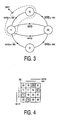
- FIG. 3 A state transition diagram of this logic function is shown in Figure 3 . From the state transition diagram a karnaugh map is derived which is shown in Figure 4 . The karnaughmap is translated directly in compound logic circuit implementations for bits R and S. consider the following situation. Suppose the control loop is out of the regulating range and the output of the comparator comp is constantly high. When the osc signal is also high the PWM limiter logic jumps to state 11 and the output pwm is high. Now when osc goes low the logic jumps to state 10 and pwm remains high. Then when osc goes high again the logic jumps to state 00 causing pwm to go low but then immediately jumps to state 11 causing pwm to go high again.
- the pwm signal shows a very short pulse which should cause the output of the switching unit to also show a (minimal) length pulse.
- the purpose of the PWM limiter is lost if the pwm pulse is not detected by the switching unit.
- a handshake can be used. The handshake is organized in such a way that in the previous example the PWM limiter logic remains instate 00 until the transition of the pwm signal has been confirmed from the switching unit. This confirmation is obtained from the release signal.
- the logic implementation of the PWM limiter is shown in Figure 5 .
- enablepower low the switching unit is inactive and release is constantly high in this case the pwm signal is fed back directly and no handshaking is done with the switching unit.
- enablepower high the switching unit is active.
- release is fed back instead of pwm.
- the release signal follows the pwm signal with a small delay. Consequently the timing of the PWM limiter logic is synchronized with the carrousel.
- the PWM limiter limits the maximal length of an output pulse by comparing it to the period of the oscillator.
- FIG 6 a part of an example of the push-pull amplifier (see also Figure 1 ) is shown.
- the input unit IU6 receives the input signal.
- the pulse width modulator PWM6 a pulse width modulated signal is obtained to overcome the problems of prior art push-pull amplifiers between the pulse width modulator PWM6 and the switching unit SU6 a pulse width modulator limiter PLIM6 is placed, whereby the logic operates as described above.
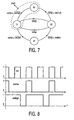
- Figure 7 shows an amended state diagram with two signals osclow and oschigh from the oscillator signal osc.
- Figure 8 shows the corresponding timing signals.
- the number of switchings is divided by two so further improving the performance of the amplifier and reducing the EMC.
Landscapes
- Engineering & Computer Science (AREA)
- Power Engineering (AREA)
- Amplifiers (AREA)
- Error Detection And Correction (AREA)
- Inverter Devices (AREA)
Claims (6)
- Gegentaktverstärker, der einen Eingang zum Empfangen eines Eingangssignals und einen Ausgang zur Bereitstellung eines Ausgangssignals aufweist, wobei der Gegentaktverstärker umfasst:einen Impulsbreitenmodulator (PWM), der wenigstens zwei Integratoren (FI, SI), einen Komparator (COM) zum Bereitstellen eines Komparatorausgangssignals (comp) und ein Rückkopplungselement (RF) umfasst,eine Schalteinheit (SU, SU6), die wenigstens zwei Schalter (SW1, SW2) aufweist, die mit dem Ausgang (Vout) der Schalteinheit gekoppelt sind,ein Demodulatorfilter (DF), das mit dem Ausgang der Schalteinheit (SU) gekoppelt ist, undeinen Impulsbreitenmodulatorbegrenzer (PLIM6) zum Begrenzen der Modulationstiefe,dadurch gekennzeichnet, dass der Impulsbreitenmodulatorbegrenzer (PLIM6) eine Logikschaltung umfasst, die an einem ersten Eingang das Komparatorausgangssignal (comp) und an einem zweiten Eingang ein Oszillatorsignal (osc) empfängt und einen dritten Eingang (release) aufweist, der mit dem Ausgang (Vout) der Schalteinheit gekoppelt ist, um eine Bestätigung von der Schalteinheit zu empfangen, dass deren Ausgang gewechselt hat.
- Gegentaktverstärker nach Anspruch 1, dadurch gekennzeichnet, dass der Gegentaktverstärker ein Klasse-D-Verstärker ist.
- Gegentaktverstärker nach Anspruch 1 oder 2, dadurch gekennzeichnet, dass der Impulsbreitenmodulatorbegrenzer (PLIN6) zwischen dem Impulsbreitenmodulator (PWM6) und der Schalteinheit (SU6) angeordnet ist.
- Gegentaktverstärker nach irgendeinem der vorangehenden Ansprüche, dadurch gekennzeichnet, dass der Impulsbreitenmodulator (PWM) ferner einen Oszillator (OSC) umfasst, und dass der wenigstens eine Integrator (FI) einen ersten Integrator (FI) und einen zweiten Integrator (SI) umfasst, wobei ein Ausgang des ersten Integrators (FI) mit einem Eingang des Impulsbreitenmodulators (PWM) gekoppelt ist, der Eingang des zweiten Integrators (SI) mit einem Ausgang des ersten Integrators und mit dem Oszillator (OSC) gekoppelt ist, und wobei der Komparator (COM) einen ersten Eingang zum Empfangen eines Ausgangssignals des ersten Integrators (FI) und einen zweiten Eingang zum Empfangen eines Ausgangssignals des zweiten Integrators (SI) aufweist.
- Gegentaktverstärker nach Anspruch 4, dadurch gekennzeichnet, dass der Oszillator (OSC) das Oszillatorsignal (osc) bereitstellt.
- Gegentaktverstärker nach irgendeinem der vorangehenden Ansprüche, dadurch gekennzeichnet, dass das Rückkopplungselement (RF) mit einer Seite an einen Ausgang der Schalteinheit (SU) und mit der anderen Seite an einen Eingang des Impulsbreitenmodulators (PWM) gekoppelt ist.
Priority Applications (1)
| Application Number | Priority Date | Filing Date | Title |
|---|---|---|---|
| EP01940395A EP1293038B1 (de) | 2000-05-25 | 2001-05-03 | Pwm-begrenzungsanordnung |
Applications Claiming Priority (4)
| Application Number | Priority Date | Filing Date | Title |
|---|---|---|---|
| EP00201828 | 2000-05-25 | ||
| EP00201828 | 2000-05-25 | ||
| PCT/EP2001/004997 WO2001091284A1 (en) | 2000-05-25 | 2001-05-03 | Pwm limiter |
| EP01940395A EP1293038B1 (de) | 2000-05-25 | 2001-05-03 | Pwm-begrenzungsanordnung |
Publications (2)
| Publication Number | Publication Date |
|---|---|
| EP1293038A1 EP1293038A1 (de) | 2003-03-19 |
| EP1293038B1 true EP1293038B1 (de) | 2009-04-15 |
Family
ID=8171536
Family Applications (1)
| Application Number | Title | Priority Date | Filing Date |
|---|---|---|---|
| EP01940395A Expired - Lifetime EP1293038B1 (de) | 2000-05-25 | 2001-05-03 | Pwm-begrenzungsanordnung |
Country Status (7)
| Country | Link |
|---|---|
| US (1) | US6577186B2 (de) |
| EP (1) | EP1293038B1 (de) |
| JP (1) | JP2003534691A (de) |
| KR (1) | KR100809241B1 (de) |
| AT (1) | ATE429070T1 (de) |
| DE (1) | DE60138382D1 (de) |
| WO (1) | WO2001091284A1 (de) |
Families Citing this family (18)
| Publication number | Priority date | Publication date | Assignee | Title |
|---|---|---|---|---|
| FR2812478B1 (fr) * | 2000-07-27 | 2003-01-10 | Rene Lambruschi | Circuit electronique de conversion d'un signal et amplificateur integrant ledit circuit |
| JP2002299968A (ja) * | 2001-03-30 | 2002-10-11 | Pioneer Electronic Corp | D級アンプ |
| AT411415B (de) * | 2001-12-11 | 2003-12-29 | Bier Guenther Ing | Verfahren und vorrichtung zur erzeugung einer einem eingangs-datenstrom folgenden wechselspannung |
| US7038535B2 (en) * | 2003-03-29 | 2006-05-02 | Wai Laing Lee | PWM digital amplifier with high-order loop filter |
| US7271650B2 (en) * | 2004-03-26 | 2007-09-18 | Asp Technologies | PWM digital amplifier with high-order loop filter |
| US7516114B2 (en) * | 2004-10-22 | 2009-04-07 | International Business Machines Corporation | Visual structuring of multivariable data |
| US7218173B2 (en) * | 2005-04-08 | 2007-05-15 | Maxim Integrated Products, Inc. | Minimum on time, dual supply class D amplifiers with ground speaker returns and methods of class D amplification |
| US20080204132A1 (en) * | 2005-04-15 | 2008-08-28 | Koninklijke Philips Electronics, N.V. | Class-D Amplifier |
| JP2010504004A (ja) * | 2006-07-07 | 2010-02-04 | エヌエックスピー ビー ヴィ | D級音声増幅器 |
| US7518442B1 (en) * | 2006-10-10 | 2009-04-14 | National Semiconductor Corporation | Circuit and method for suppressing switching and supply-related errors in a PWM power stage by instantaneous per-pulse feedback |
| US8081022B2 (en) * | 2007-03-14 | 2011-12-20 | Nxp B.V. | Data processing system for clipping correction |
| US8067980B2 (en) * | 2007-06-27 | 2011-11-29 | Nxp B.V. | Pulse width modulation circuit and class-D amplifier comprising the PWM circuit |
| JP2011097504A (ja) * | 2009-11-02 | 2011-05-12 | Hitachi Kokusai Electric Inc | 電源回路 |
| KR101728185B1 (ko) * | 2009-10-28 | 2017-04-18 | 가부시키가이샤 한도오따이 에네루기 켄큐쇼 | Pwm 리미터 회로 |
| EP2562933A1 (de) | 2011-08-25 | 2013-02-27 | Nxp B.V. | Verstärker der Klasse D und Steuerverfahren |
| WO2016162156A1 (en) * | 2015-04-09 | 2016-10-13 | Bang & Olufsen Icepower A/S | Duty cycle clipper |
| US11646707B2 (en) * | 2020-05-21 | 2023-05-09 | Novatek Microelectronics Corp. | Analog front end with pulse width modulation current compensation |
| US11463052B2 (en) | 2020-11-30 | 2022-10-04 | Stmicroelectronics S.R.L. | PWM driving circuit and method |
Family Cites Families (4)
| Publication number | Priority date | Publication date | Assignee | Title |
|---|---|---|---|---|
| US5389829A (en) * | 1991-09-27 | 1995-02-14 | Exar Corporation | Output limiter for class-D BICMOS hearing aid output amplifier |
| US5777512A (en) * | 1996-06-20 | 1998-07-07 | Tripath Technology, Inc. | Method and apparatus for oversampled, noise-shaping, mixed-signal processing |
| US5974089A (en) * | 1997-07-22 | 1999-10-26 | Tripath Technology, Inc. | Method and apparatus for performance improvement by qualifying pulses in an oversampled noise-shaping signal processor |
| EP0968565A2 (de) * | 1998-01-22 | 2000-01-05 | Koninklijke Philips Electronics N.V. | Pulsbreitenmodulationsverstärker |
-
2001
- 2001-05-03 AT AT01940395T patent/ATE429070T1/de not_active IP Right Cessation
- 2001-05-03 WO PCT/EP2001/004997 patent/WO2001091284A1/en not_active Ceased
- 2001-05-03 JP JP2001586769A patent/JP2003534691A/ja not_active Withdrawn
- 2001-05-03 EP EP01940395A patent/EP1293038B1/de not_active Expired - Lifetime
- 2001-05-03 KR KR1020027000955A patent/KR100809241B1/ko not_active Expired - Fee Related
- 2001-05-03 DE DE60138382T patent/DE60138382D1/de not_active Expired - Lifetime
- 2001-05-24 US US09/864,140 patent/US6577186B2/en not_active Expired - Lifetime
Also Published As
| Publication number | Publication date |
|---|---|
| US6577186B2 (en) | 2003-06-10 |
| US20020000877A1 (en) | 2002-01-03 |
| JP2003534691A (ja) | 2003-11-18 |
| DE60138382D1 (de) | 2009-05-28 |
| KR20020056874A (ko) | 2002-07-10 |
| ATE429070T1 (de) | 2009-05-15 |
| KR100809241B1 (ko) | 2008-02-29 |
| EP1293038A1 (de) | 2003-03-19 |
| WO2001091284A1 (en) | 2001-11-29 |
Similar Documents
| Publication | Publication Date | Title |
|---|---|---|
| US6577186B2 (en) | PWM limiter | |
| EP3687065B1 (de) | Hüllkurvennachführungsmodulator | |
| KR100939728B1 (ko) | 엔벨로프 제거 및 복원 송신기 구조와 함께 사용하기 위한가변 대역폭 엔벨로프 변조기 및 엔벨로프 제거 및 복원송신기용 방법 | |
| US7965141B2 (en) | Class D audio amplifier | |
| CN100527605C (zh) | 放大器及使用它的高频功率放大器 | |
| US6498531B1 (en) | Digital class-D audio amplifier | |
| US7394233B1 (en) | High efficiency modulated power supply | |
| US20020097091A1 (en) | Class D audio amplifier | |
| US10560082B2 (en) | Pulse width modulation circuit, corresponding device and method | |
| WO2007147240A1 (en) | Integrated implementation of a voltage boost follower and method therefor | |
| US6351184B1 (en) | Dynamic switching frequency control for a digital switching amplifier | |
| JPH10163764A (ja) | 広帯域クラスs変調器およびその方法 | |
| AU3451900A (en) | Class d digital amplifier | |
| EP3223427A1 (de) | Selbstschwingender klasse-d verstärker | |
| EP1184973A1 (de) | Leistungsverstärkervorrichtung | |
| US6384678B2 (en) | Silent start | |
| AU2740301A (en) | Active isolated-integrator low-pass filter with attenuation poles | |
| JPH0246417U (de) | ||
| JPH06196940A (ja) | パルス幅変調増幅回路 | |
| CN208638335U (zh) | 一种适用于pwm功放的反馈调节跳脉冲保护装置 | |
| KR101065903B1 (ko) | 발진기를 이용한 고효율 선형 전력증폭 시스템 | |
| JPH0779266B2 (ja) | 送信出力制御回路 | |
| JPH01256229A (ja) | シンセサイザ変調装置 |
Legal Events
| Date | Code | Title | Description |
|---|---|---|---|
| PUAI | Public reference made under article 153(3) epc to a published international application that has entered the european phase |
Free format text: ORIGINAL CODE: 0009012 |
|
| 17P | Request for examination filed |
Effective date: 20021227 |
|
| AK | Designated contracting states |
Kind code of ref document: A1 Designated state(s): AT BE CH CY DE DK ES FI FR GB GR IE IT LI LU MC NL PT SE TR |
|
| 17Q | First examination report despatched |
Effective date: 20060524 |
|
| RAP1 | Party data changed (applicant data changed or rights of an application transferred) |
Owner name: NXP B.V. |
|
| GRAP | Despatch of communication of intention to grant a patent |
Free format text: ORIGINAL CODE: EPIDOSNIGR1 |
|
| GRAS | Grant fee paid |
Free format text: ORIGINAL CODE: EPIDOSNIGR3 |
|
| GRAA | (expected) grant |
Free format text: ORIGINAL CODE: 0009210 |
|
| AK | Designated contracting states |
Kind code of ref document: B1 Designated state(s): AT BE CH CY DE DK ES FI FR GB GR IE IT LI LU MC NL PT SE TR |
|
| REG | Reference to a national code |
Ref country code: GB Ref legal event code: FG4D Ref country code: CH Ref legal event code: EP |
|
| REG | Reference to a national code |
Ref country code: IE Ref legal event code: FG4D |
|
| REF | Corresponds to: |
Ref document number: 60138382 Country of ref document: DE Date of ref document: 20090528 Kind code of ref document: P |
|
| NLV1 | Nl: lapsed or annulled due to failure to fulfill the requirements of art. 29p and 29m of the patents act | ||
| PG25 | Lapsed in a contracting state [announced via postgrant information from national office to epo] |
Ref country code: ES Free format text: LAPSE BECAUSE OF FAILURE TO SUBMIT A TRANSLATION OF THE DESCRIPTION OR TO PAY THE FEE WITHIN THE PRESCRIBED TIME-LIMIT Effective date: 20090726 Ref country code: FI Free format text: LAPSE BECAUSE OF FAILURE TO SUBMIT A TRANSLATION OF THE DESCRIPTION OR TO PAY THE FEE WITHIN THE PRESCRIBED TIME-LIMIT Effective date: 20090415 Ref country code: PT Free format text: LAPSE BECAUSE OF FAILURE TO SUBMIT A TRANSLATION OF THE DESCRIPTION OR TO PAY THE FEE WITHIN THE PRESCRIBED TIME-LIMIT Effective date: 20090915 Ref country code: AT Free format text: LAPSE BECAUSE OF FAILURE TO SUBMIT A TRANSLATION OF THE DESCRIPTION OR TO PAY THE FEE WITHIN THE PRESCRIBED TIME-LIMIT Effective date: 20090415 |
|
| PG25 | Lapsed in a contracting state [announced via postgrant information from national office to epo] |
Ref country code: SE Free format text: LAPSE BECAUSE OF FAILURE TO SUBMIT A TRANSLATION OF THE DESCRIPTION OR TO PAY THE FEE WITHIN THE PRESCRIBED TIME-LIMIT Effective date: 20090715 Ref country code: NL Free format text: LAPSE BECAUSE OF FAILURE TO SUBMIT A TRANSLATION OF THE DESCRIPTION OR TO PAY THE FEE WITHIN THE PRESCRIBED TIME-LIMIT Effective date: 20090415 |
|
| PG25 | Lapsed in a contracting state [announced via postgrant information from national office to epo] |
Ref country code: MC Free format text: LAPSE BECAUSE OF NON-PAYMENT OF DUE FEES Effective date: 20090531 |
|
| REG | Reference to a national code |
Ref country code: CH Ref legal event code: PL |
|
| PG25 | Lapsed in a contracting state [announced via postgrant information from national office to epo] |
Ref country code: LI Free format text: LAPSE BECAUSE OF NON-PAYMENT OF DUE FEES Effective date: 20090531 Ref country code: DK Free format text: LAPSE BECAUSE OF FAILURE TO SUBMIT A TRANSLATION OF THE DESCRIPTION OR TO PAY THE FEE WITHIN THE PRESCRIBED TIME-LIMIT Effective date: 20090415 Ref country code: CH Free format text: LAPSE BECAUSE OF NON-PAYMENT OF DUE FEES Effective date: 20090531 |
|
| PLBE | No opposition filed within time limit |
Free format text: ORIGINAL CODE: 0009261 |
|
| STAA | Information on the status of an ep patent application or granted ep patent |
Free format text: STATUS: NO OPPOSITION FILED WITHIN TIME LIMIT |
|
| PG25 | Lapsed in a contracting state [announced via postgrant information from national office to epo] |
Ref country code: BE Free format text: LAPSE BECAUSE OF FAILURE TO SUBMIT A TRANSLATION OF THE DESCRIPTION OR TO PAY THE FEE WITHIN THE PRESCRIBED TIME-LIMIT Effective date: 20090415 |
|
| REG | Reference to a national code |
Ref country code: IE Ref legal event code: MM4A |
|
| 26N | No opposition filed |
Effective date: 20100118 |
|
| PG25 | Lapsed in a contracting state [announced via postgrant information from national office to epo] |
Ref country code: IE Free format text: LAPSE BECAUSE OF NON-PAYMENT OF DUE FEES Effective date: 20090503 |
|
| PG25 | Lapsed in a contracting state [announced via postgrant information from national office to epo] |
Ref country code: GR Free format text: LAPSE BECAUSE OF FAILURE TO SUBMIT A TRANSLATION OF THE DESCRIPTION OR TO PAY THE FEE WITHIN THE PRESCRIBED TIME-LIMIT Effective date: 20090716 |
|
| PG25 | Lapsed in a contracting state [announced via postgrant information from national office to epo] |
Ref country code: IT Free format text: LAPSE BECAUSE OF FAILURE TO SUBMIT A TRANSLATION OF THE DESCRIPTION OR TO PAY THE FEE WITHIN THE PRESCRIBED TIME-LIMIT Effective date: 20090415 |
|
| PG25 | Lapsed in a contracting state [announced via postgrant information from national office to epo] |
Ref country code: LU Free format text: LAPSE BECAUSE OF NON-PAYMENT OF DUE FEES Effective date: 20090503 |
|
| PG25 | Lapsed in a contracting state [announced via postgrant information from national office to epo] |
Ref country code: TR Free format text: LAPSE BECAUSE OF FAILURE TO SUBMIT A TRANSLATION OF THE DESCRIPTION OR TO PAY THE FEE WITHIN THE PRESCRIBED TIME-LIMIT Effective date: 20090415 |
|
| PG25 | Lapsed in a contracting state [announced via postgrant information from national office to epo] |
Ref country code: CY Free format text: LAPSE BECAUSE OF FAILURE TO SUBMIT A TRANSLATION OF THE DESCRIPTION OR TO PAY THE FEE WITHIN THE PRESCRIBED TIME-LIMIT Effective date: 20090415 |
|
| REG | Reference to a national code |
Ref country code: FR Ref legal event code: PLFP Year of fee payment: 15 |
|
| REG | Reference to a national code |
Ref country code: FR Ref legal event code: PLFP Year of fee payment: 16 |
|
| REG | Reference to a national code |
Ref country code: FR Ref legal event code: PLFP Year of fee payment: 17 |
|
| REG | Reference to a national code |
Ref country code: FR Ref legal event code: PLFP Year of fee payment: 18 |
|
| PGFP | Annual fee paid to national office [announced via postgrant information from national office to epo] |
Ref country code: DE Payment date: 20200421 Year of fee payment: 20 Ref country code: FR Payment date: 20200422 Year of fee payment: 20 |
|
| PGFP | Annual fee paid to national office [announced via postgrant information from national office to epo] |
Ref country code: GB Payment date: 20200423 Year of fee payment: 20 |
|
| REG | Reference to a national code |
Ref country code: DE Ref legal event code: R071 Ref document number: 60138382 Country of ref document: DE |
|
| REG | Reference to a national code |
Ref country code: GB Ref legal event code: PE20 Expiry date: 20210502 |
|
| PG25 | Lapsed in a contracting state [announced via postgrant information from national office to epo] |
Ref country code: GB Free format text: LAPSE BECAUSE OF EXPIRATION OF PROTECTION Effective date: 20210502 |