EP1294028A1 - Lichtemittierendes halbleiterbauelement, verfahren zur herstellung eines lichtemittierenden halbleiterbauelements und elektrodenschichtverbindungsstruktur - Google Patents
Lichtemittierendes halbleiterbauelement, verfahren zur herstellung eines lichtemittierenden halbleiterbauelements und elektrodenschichtverbindungsstruktur Download PDFInfo
- Publication number
- EP1294028A1 EP1294028A1 EP02711454A EP02711454A EP1294028A1 EP 1294028 A1 EP1294028 A1 EP 1294028A1 EP 02711454 A EP02711454 A EP 02711454A EP 02711454 A EP02711454 A EP 02711454A EP 1294028 A1 EP1294028 A1 EP 1294028A1
- Authority
- EP
- European Patent Office
- Prior art keywords
- layer
- semiconductor
- light emitting
- emitting device
- semiconductor light
- Prior art date
- Legal status (The legal status is an assumption and is not a legal conclusion. Google has not performed a legal analysis and makes no representation as to the accuracy of the status listed.)
- Granted
Links
Images

Classifications
-
- H—ELECTRICITY
- H10—SEMICONDUCTOR DEVICES; ELECTRIC SOLID-STATE DEVICES NOT OTHERWISE PROVIDED FOR
- H10H—INORGANIC LIGHT-EMITTING SEMICONDUCTOR DEVICES HAVING POTENTIAL BARRIERS
- H10H20/00—Individual inorganic light-emitting semiconductor devices having potential barriers, e.g. light-emitting diodes [LED]
- H10H20/80—Constructional details
- H10H20/83—Electrodes
- H10H20/832—Electrodes characterised by their material
- H10H20/835—Reflective materials
-
- H—ELECTRICITY
- H10—SEMICONDUCTOR DEVICES; ELECTRIC SOLID-STATE DEVICES NOT OTHERWISE PROVIDED FOR
- H10H—INORGANIC LIGHT-EMITTING SEMICONDUCTOR DEVICES HAVING POTENTIAL BARRIERS
- H10H20/00—Individual inorganic light-emitting semiconductor devices having potential barriers, e.g. light-emitting diodes [LED]
- H10H20/80—Constructional details
- H10H20/81—Bodies
- H10H20/822—Materials of the light-emitting regions
- H10H20/824—Materials of the light-emitting regions comprising only Group III-V materials, e.g. GaP
- H10H20/825—Materials of the light-emitting regions comprising only Group III-V materials, e.g. GaP containing nitrogen, e.g. GaN
Definitions
- This invention relates to a semiconductor light emitting device made by using nitride semiconductors or the like, its manufacturing method, and a connection structure of an electrode layer. More particularly, the invention relates to a semiconductor light emitting device of the type that reflects light generated in the active layer with an electrode layer deposited on the active layer, its manufacturing method, and a connection structure of the electrode layer.
- Gallium nitride-family compound semiconductors are increasing their use as semiconductor materials for visible light emitting devices, and their development is progressing especially in the field of blue and green light emitting diodes.
- Light emitting diodes in general, have a structure of sequential deposition of n-type semiconductor layers, active layers and p-type semiconductor layers by crystal growth of gallium nitride-family compound semiconductor layers on a sapphire substrate, or the like. In case of a light emitting diode having this kind of multi-layered structure, electric current is introduced to the active layer, and light generated in the active layer is externally taken out.
- semiconductor light emitting devices of this type there are known structures configured to extract light traveling upward of the active layer and structures configured to extract light traveling downward of the active layer through a transparent substrate.
- structures configured to extract light through a transparent substrate there is a device having a structure using an electrode connected to a p-type semiconductor layer as a reflective layer.
- a light emitting diode device disclosed in Japanese Patent Laid-Open Publication No. hei 11-191641 a light emitting diode device disclosed in Japanese Patent Laid-Open Publication No. hei 11-220170
- a semiconductor light emitting device disclosed in Japanese Patent Laid-Open Publication No. 2000-91638 are known among others.
- the thickness of the contact layer is as thick as approximately 50 nm, for example, it is difficult to enhance the reflectance, and it needs improvement of the reflection structure itself, including the contact metal layer under the demand for higher and higher light emitting efficiency.
- a semiconductor light emitting device including a semiconductor light emitting layer of a first conduction type, an active layer and a semiconductor layer of a second conduction type which are sequentially deposited on an optically transparent substrate, comprises: an electrode layer formed on the semiconductor layer of the second conduction type on the active layer, and a contact metal layer interposed between the electrode layer and the semiconductor layer of the second conduction type and adjusted in thickness not to exceed the intrusion length of light emitted generated in the active layer.
- the active layer can generate light with a current injected therein. Since the substrate is optically transparent, the light generated in the active layer is radiated through the substrate, but part of the light generated in the active layer travels toward the semiconductor layer of the second conduction type. Since the electrode layer overlies the semiconductor layer of the second conduction type, their interface can reflect the light traveling toward this semiconductor layer. Thus the light traveling toward the semiconductor layer of the second conduction type is reflected toward the substrate.
- the contact metal layer is interposed between the electrode layer and the semiconductor layer of the second conduction type and adjusted in thickness not to exceed the intrusion length of the generated light, reflectance by the electrode layer can be enhanced while the ohmic contact is ensured, and the emission efficiency of the entire device can be enhanced accordingly.
- a method of manufacturing a semiconductor light emitting device comprises the steps of: sequentially depositing a semiconductor light emitting layer of a first conduction type, an active layer and a semiconductor layer of a second conduction type on an optically transparent substrate; forming a contact metal layer on the semiconductor layer of the second conduction type, which is adjusted in thickness not to exceed the intrusion length of light generated in the active layer; and forming an electrode layer on the contact metal layer.
- the contact metal layer adjusted in thickness not to exceed the intrusion length of the light generated in the active layer after the semiconductor layer of the second conduction type is formed, and the electrode layer is formed after the contact metal layer having that thickness is formed. Therefore, the contact metal layer having the thickness not exceeding the intrusion length of the light generated in the active layer can enhance the reflectance by the electrode layer while the ohmic contact is ensured, and the intensity of reflection toward the optically transparent substrate can be enhanced accordingly.
- a connection structure of an electrode layer according to the invention comprises: an optically transparent semiconductor layer; a contact metal layer formed on the semiconductor layer and adjusted in thickness not to exceed the intrusion length of light passing through the semiconductor layer; and an electrode layer formed on the contact metal layer.
- Fig. 1 is a cross-sectional view of a semiconductor light emitting device according to the instant embodiment of the invention.
- the semiconductor light emitting device according to the first embodiment includes a light emitting portion formed by stacking GaN compound semiconductors. Namely, on a insulating transparent sapphire substrate 11 via a GaN buffer layer, an n-type GaN layer 12 doped with silicon, InGaN active layer 13 for emitting light, and p-type GaN layer 14 doped with magnesium are stacked.
- the silicon-doped n-type GaN layer 12 functions as a cladding layer of the first conduction type
- the magnesium-doped p-type GaN layer 14 functions as the cladding layer of the second conduction type.
- the device has a double-hetero structure.
- a nickel layer 15 as a contact metal layer for ohmic contact is formed on the p-type GaN layer 14 as the cladding layer of the second conduction type. Thickness of the nickel layer 15 is adjusted not to exceed the intrusion length of light generated in the active layer as explained later. In this embodiment, the thickness is approximately 10 nm, for example.
- a p-side electrode layer 16 is a thin film of aluminum or silver such that the light passing through the nickel layer 15 as the contact metal layer is reflected by the interface with the p-side electrode layer 16.
- the p-side electrode layer 16 used in this embodiment is a thin film of aluminum or silver, it may be a metal layer of gold or platinum on the aluminum or silver thin film.
- the n-side electrode 18 is formed by first stacking the n-type GaN layer 12, InGaN active layer 13 and p-type GaN layer 14 on the entire surface, thereafter forming an n-side electrode extracting region 17 where the n-type GaN layer 12 is exposed by making an opening, so as to lie on the n-side electrode extracting region 17 for electrical connection with the n-type GaN layer 12.
- the n-side electrode layer 18 has a Ti/Al/Pt/Au electrode structure.
- Fig. 2 is a cross-sectional view of the substantial part of the first embodiment of the invention.
- the semiconductor light emitting device according to the instant embodiment has a double-hetero structure interposing an InGaN active layer 13 between the n-type GaN layer 12 and the p-type GaN layer 14 that are cladding layers.
- the nickel layer 15 as the contact metal layer for making ohmic contact is formed on the p-type GaN layer 14, and the p-side electrode layer 16 of aluminum or silver is formed on the nickel layer 15. Thickness t of the nickel layer 15 is adjusted not to exceed the intrusion length ⁇ of light generated in the active layer 13.
- the thickness is approximately 10 nm in this embodiment, but may be changed in accordance with light to be generated, or may be changed in accordance with the quality of the film upon being formed by vapor deposition or plating, for example.
- the light When light is reflected by a metal surface, the light as a electromagnetic wave having an energy enters into the metal from its surface by the depth called intrusion length from the metal surface. In case of complete reflection, the light reflects while receiving the same energy by phonon interaction.
- ohmic contact can be attained even with an extremely thin film.
- Emitting operation has been confirmed even with a nickel layer 15 as extremely thin as 1 nm through an experiment by the Inventor. As such, when the thickness t of the nickel layer 15 is adjusted not to exceed the intrusion length ⁇ of light generated in the active layer 13, reflection efficiency of the overlying p-type GaN layer 14 can be enhanced.
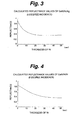
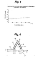
- the thickness t of the nickel layer 15 is preferably not thicker than 20 nm, more preferably not thicker than 10 nm, and more preferably not thicker than 5 nm. Such ranges of the thickness t can be explained also from diagrams of Figs. 3 through 5 that show relationships between thickness of the nickel layer and reflectance.
- Fig. 3 shows calculated values of reflectance obtained by reflecting emitted light while changing thickness of the Ni layer in a multi-layered structure including GaN, Ni and Ag layers.
- the reflectance is higher when the Ni layer is thin, and tends to decrease as the Ni layer becomes thicker.
- the corresponding reflectance is 0.4 or less in absolute value. Therefore, in order to attain reflectance not less than 0.4, thickness of the Ni layer must be limited not to exceed 20 nm, and preferably, it is limited not to exceed 10 nm. If a reflectance of 0.6 or more is desirable, thickness of the Ni layer is preferably limited not to exceed 5 nm.
- Fig. 4 shows calculated values of reflectance obtained by reflecting emitted light while changing thickness of the Ni layer in a multi-layered structure including GaN, Ni and Al layers.
- the reflectance is higher when the Ni layer is thin, and tends to decrease as the Ni layer becomes thicker.
- the corresponding reflectance is 0.5 or less in absolute value. Therefore, in order to attain reflectance not less than 0.5, thickness of the Ni layer must be limited not to exceed 20 nm, and preferably, it is limited not to exceed 10 nm.
- the reflectance becomes 0.6 or more only when the thickness is 10 nm or less. More preferably, therefore, thickness of the Ni layer is preferably adjusted not to exceed 5 nm.
- Fig. 5 is a diagram showing calculated values of reflectance of a multi-layered structure including GaN, Ni and Au layers. This structure using Au as the electrode layer does not exhibit the tendency of increasing reflectance even when the Ni layer is thinned. By comparison with Fig. 5, it is apparent that preferable metal material of the p-side electrode is Ag or Al.
- the semiconductor light emitting device configured to extract light through the transparent sapphire substrate 11
- the light output from the InGaN active layer 13 is the sum of the light directly passing through the n-type GaN layer 12 and the sapphire substrate 11 and the light reflected back from the p-side electrode layer 16, and reflection efficiency of the light from the p-side electrode layer 16 is enhanced by thinning and optimizing the nickel layer 15 as the contact metal layer, emission efficiency of the device as a whole can be realized.
- the foregoing embodiment has been explained as using the sapphire substrate as its substrate, other optically transparent substrates are also usable, such as gallium nitride substrate, glass substrate, transparent resin substrate, etc. It is also possible to use a substrate for mounting separately from a substrate by crystal growth by transfer, for example.
- the contact metal layer having explained as being Ni may be made of Pd, Co, Sb, or the like, or any of the alloys.
- This embodiment is directed to a semiconductor light emitting device having a six-sided-pyramidal crystal portion by selective growth.
- the semiconductor light emitting device has the structure having a growth-inhibiting film 23 in form of a silicon oxide film, for example, formed on a base growth layer 22, and an n-type GaN layer 25 formed by selective growth from a window 24 made by partly opening the growth-inhibiting film 23.
- the base growth layer 22 is a layer grown to stack on a sapphire substrate having a c-oriented major surface via a buffer layer, and separated from the sapphire substrate by laser abrasion between the sapphire substrate and the base growth layer 22 by laser irradiation from beyond the bottom surface of the sapphire substrate.
- n-type GaN layer 25 grown from the base growth layer 22 into a six-sided pyramid or a quadrangular pyramid, and S-oriented slanted planes surround its perimeters.
- An InGaN active layer 26 is formed on the n-type GaN layer 25, and a magnesium-doped p-type GaN layer 27 is further stacked thereon.
- the n-type GaN layer 25 functions as the cladding layer of the first conduction type
- the p-type GaN layer 27 functions as the cladding layer of the second conduction type.
- the semiconductor light emitting device according to the instant embodiment has a double-hetero structure.
- a nickel layer 28 is formed as the contact metal layer so as to cover the slanted surfaces, and a p-side electrode layer 29 is made of a metal material such as Ag or Al on the nickel layer 28.
- the nickel layer shown with a line in Fig. 6 is a thin film for the purpose of ohmic contact. Thickness of the nickel layer 28 is adjusted not to exceed the intrusion length of light generated in the active layer. It is approximately 10 nm, for example, in this embodiment.
- the p-side electrode layer 29 overlying the nickel layer 28 is used for reflecting light passing through the nickel layer 28 at the interface of the p-side electrode layer 29.
- the p-side electrode layer 29 enclose the InGaN active layer 26 in a self-aligned manner to form a structure like a reflector having its center at the apex of the six-sided pyramid such that light can be efficiently extracted while being multiply reflected. Therefore, by adjusting the thickness of the nickel layer 28 not to exceed the intrusion length of light generated in the InGaN active layer 26, it is possible to enhance the reflectance at the reflective surfaces and to increase the throughput of light.
- An experiment by the Inventors gave data that this structure with the nickel layer 28 controlled in thickness not to exceed the intrusion length of light exhibits emission efficiency as high as approximately 1.7 times that of a structures not controlled in thickness of the nickel layer 28.
- Part of the base growth layer 22 is horizontally extended longer than the bottom of the n-type GaN layer 25.
- the growth-inhibiting film 23 is partly removed to form an opening 30, and an n-side electrode layer 31 is formed inside the opening 30.
- the n-side electrode layer 31 has a Ti/Al/Pt/Au electrode structure, for example.
- the p-side electrode layer 16 is a thin film of aluminum or silver, for example, but it may have a structure including a metal layer of gold, platinum, or the like, stacked on an aluminum or silver layer.
- the light output from the InGaN active layer 26 is the sum of the light directly passing through the n-type GaN layer 25 and the base growth layer 22 and the light reflected back from the p-side electrode layer 29, and reflection efficiency of the light from the p-side electrode layer 29 is enhanced by thinning and optimizing the nickel layer 28 as the contact metal layer, emission efficiency of the device as a whole can be realized.
- the six-sided-pyramidal crystal structure is obtained by selective growth and the p-side electrode layer 29 formed in self alignment on the slanted surfaces of S-oriented planes, for example, of the GaN layer functions as a reflective film causing multiplex reflection, still higher reflectance can be realized.
- the invention is applicable also to semiconductor lasers and other optical semiconductor devices.
- the semiconductor light emitting devices according to the invention are not limited in emission wavelength, in case of a device for emitting blue light, the p-side electrode layer is preferably made of Ag or Al.
- the contact metal layer having explained as being made of Ni may be made of Pd, Co or Sb, or any of their alloys instead.
- the semiconductor light emitting device of the invention since the light extracted through the transparent substrate is the sum of the light directly passing through the n-type GaN layer from the active layer and the light reflected back from the p-side electrode layer, and reflection efficiency of the light from the p-side electrode layer is enhanced by thinning and optimizing the contact metal layer, emission efficiency of the device as a whole can be easily realized.
- the semiconductor layers are formed by selective growth, since a pyramidal crystal structure in form of a six-sides pyramid, for example, can be obtained, and the p-side electrode layer formed in self alignment on the slanted surfaces of S-oriented planes, for example, of the GaN layer functions as a reflective film causing multiplex reflection, still higher reflectance can be realized.
Landscapes
- Led Devices (AREA)
Applications Claiming Priority (3)
| Application Number | Priority Date | Filing Date | Title |
|---|---|---|---|
| JP2001044832A JP5283293B2 (ja) | 2001-02-21 | 2001-02-21 | 半導体発光素子 |
| JP2001044832 | 2001-02-21 | ||
| PCT/JP2002/001134 WO2002067340A1 (en) | 2001-02-21 | 2002-02-12 | Semiconductor light-emitting device, method for fabricating semiconductor light-emitting device, and electrode layer connection structure |
Publications (3)
| Publication Number | Publication Date |
|---|---|
| EP1294028A1 true EP1294028A1 (de) | 2003-03-19 |
| EP1294028A4 EP1294028A4 (de) | 2009-04-01 |
| EP1294028B1 EP1294028B1 (de) | 2020-04-01 |
Family
ID=18906750
Family Applications (1)
| Application Number | Title | Priority Date | Filing Date |
|---|---|---|---|
| EP02711454.5A Expired - Lifetime EP1294028B1 (de) | 2001-02-21 | 2002-02-12 | Lichtemittierendes halbleiterbauelement und verfahren zu seiner herstellung |
Country Status (7)
| Country | Link |
|---|---|
| US (1) | US6831300B2 (de) |
| EP (1) | EP1294028B1 (de) |
| JP (1) | JP5283293B2 (de) |
| KR (1) | KR100839179B1 (de) |
| CN (1) | CN100350636C (de) |
| TW (1) | TW535306B (de) |
| WO (1) | WO2002067340A1 (de) |
Cited By (5)
| Publication number | Priority date | Publication date | Assignee | Title |
|---|---|---|---|---|
| WO2004084320A3 (en) * | 2003-03-19 | 2005-04-14 | Gelcore Llc | Flip-chip light emitting diode with a thermally stable multiple layer reflective p-type contact |
| EP1511091A3 (de) * | 2003-08-25 | 2006-12-13 | Samsung Electronics Co., Ltd. | Lichtemittierende Halbleitervorrichtung aus einer Nitridverbindung und Herstellungsverfahren |
| CN100403557C (zh) * | 2003-04-21 | 2008-07-16 | 三星电机株式会社 | 半导体发光二极管及其制造方法 |
| WO2007138527A3 (en) * | 2006-05-25 | 2008-09-12 | Koninkl Philips Electronics Nv | Reflective electrode for a semiconductor light emitting apparatus |
| EP1761960A4 (de) * | 2004-06-24 | 2010-07-21 | Showa Denko Kk | Reflektierende positive elektrode und diese verwendende lichtemittierende halbleitervorrichtung aus einer galliumnitridverbindung |
Families Citing this family (23)
| Publication number | Priority date | Publication date | Assignee | Title |
|---|---|---|---|---|
| KR101034055B1 (ko) | 2003-07-18 | 2011-05-12 | 엘지이노텍 주식회사 | 발광 다이오드 및 그 제조방법 |
| JP4130163B2 (ja) * | 2003-09-29 | 2008-08-06 | 三洋電機株式会社 | 半導体発光素子 |
| TWI254469B (en) * | 2004-04-14 | 2006-05-01 | Osram Opto Semiconductors Gmbh | Luminous diode chip |
| CN100423300C (zh) * | 2004-04-29 | 2008-10-01 | 奥斯兰姆奥普托半导体有限责任公司 | 辐射发射的半导体芯片及其制造方法 |
| DE102004025610A1 (de) * | 2004-04-30 | 2005-11-17 | Osram Opto Semiconductors Gmbh | Optoelektronisches Bauelement mit mehreren Stromaufweitungsschichten und Verfahren zu dessen Herstellung |
| US20060054919A1 (en) * | 2004-08-27 | 2006-03-16 | Kyocera Corporation | Light-emitting element, method for manufacturing the same and lighting equipment using the same |
| KR101217659B1 (ko) * | 2004-09-03 | 2013-01-02 | 스탠리 일렉트릭 컴퍼니, 리미티드 | El소자 |
| JP4384019B2 (ja) * | 2004-12-08 | 2009-12-16 | 住友電気工業株式会社 | ヘッドランプ |
| KR100601992B1 (ko) | 2005-02-16 | 2006-07-18 | 삼성전기주식회사 | 반사전극 및 이를 구비하는 화합물 반도체 발광소자 |
| JP5159040B2 (ja) * | 2005-03-31 | 2013-03-06 | 株式会社光波 | 低温成長バッファ層の形成方法および発光素子の製造方法 |
| KR100638819B1 (ko) * | 2005-05-19 | 2006-10-27 | 삼성전기주식회사 | 광추출효율이 개선된 수직구조 질화물 반도체 발광소자 |
| WO2007004701A1 (en) * | 2005-07-04 | 2007-01-11 | Showa Denko K.K. | Gallium nitride-based compound semiconductor lihgt-emitting device |
| KR100755598B1 (ko) * | 2006-06-30 | 2007-09-06 | 삼성전기주식회사 | 질화물 반도체 발광소자 어레이 |
| US8236594B2 (en) * | 2006-10-20 | 2012-08-07 | Chien-Min Sung | Semiconductor-on-diamond devices and associated methods |
| JP5004337B2 (ja) * | 2007-03-06 | 2012-08-22 | シチズン電子株式会社 | メタルコア基板の外部接続端子 |
| GB2453580B (en) | 2007-10-11 | 2012-06-06 | Dall Production Aps | A Rotary encoder |
| KR101248624B1 (ko) | 2011-08-01 | 2013-03-28 | 주식회사 케이이씨 | 발광 반도체 디바이스 및 그 제조 방법 |
| JP2012169667A (ja) * | 2012-05-11 | 2012-09-06 | Toshiba Corp | 半導体発光素子及びその製造方法 |
| CN104681685A (zh) * | 2013-11-28 | 2015-06-03 | 亚世达科技股份有限公司 | 发光二极管装置及灯具 |
| CN105609611A (zh) * | 2015-09-15 | 2016-05-25 | 华南师范大学 | 倒装芯片发光二极管器件及其制造方法 |
| US11069837B2 (en) * | 2018-04-20 | 2021-07-20 | Glo Ab | Sub pixel light emitting diodes for direct view display and methods of making the same |
| CN109860368B (zh) * | 2018-11-28 | 2020-12-01 | 华灿光电(浙江)有限公司 | 一种发光二极管外延片、芯片及其制备方法 |
| CN114623418B (zh) * | 2018-12-26 | 2023-12-01 | 深圳光峰科技股份有限公司 | 一种具有高的红光亮度和高的可靠性的发光装置 |
Family Cites Families (62)
| Publication number | Priority date | Publication date | Assignee | Title |
|---|---|---|---|---|
| JPS5692577A (en) | 1979-12-26 | 1981-07-27 | Fujitsu Ltd | Lighttemittinggdiode display panel |
| JPS5745583A (en) | 1980-09-01 | 1982-03-15 | Tokyo Shibaura Electric Co | Solid state light emitting display unit |
| JPS5752072A (en) | 1980-09-16 | 1982-03-27 | Tokyo Shibaura Electric Co | Display unit |
| JPS5752071A (en) | 1980-09-16 | 1982-03-27 | Tokyo Shibaura Electric Co | Display unit |
| JPS5752073A (en) | 1980-09-16 | 1982-03-27 | Tokyo Shibaura Electric Co | Method of producing display unit |
| JPS5850577A (ja) | 1981-09-22 | 1983-03-25 | 株式会社東芝 | デイスプレイ装置 |
| JPS61156780A (ja) | 1984-12-28 | 1986-07-16 | Toshiba Corp | 発光素子整列組立体の製造方法 |
| JPS63188938A (ja) | 1987-01-31 | 1988-08-04 | Toyoda Gosei Co Ltd | 窒化ガリウム系化合物半導体の気相成長方法 |
| JP2577089B2 (ja) | 1988-11-10 | 1997-01-29 | 日本板硝子株式会社 | 発光装置およびその駆動方法 |
| EP0405757A3 (en) | 1989-06-27 | 1991-01-30 | Hewlett-Packard Company | High efficiency light-emitting diode |
| EP0410695B1 (de) * | 1989-07-25 | 2001-10-24 | Nippon Sheet Glass Co., Ltd. | Lichtemittierende Vorrichtung |
| JPH05251738A (ja) * | 1992-03-05 | 1993-09-28 | Fujitsu Ltd | 半導体光素子アレイの作製方法 |
| JPH0645648A (ja) | 1992-07-24 | 1994-02-18 | Omron Corp | 上面出射型半導体発光素子、ならびに当該発光素子を用いた光学検知装置、光学的情報処理装置及び発光装置。 |
| JPH0667044A (ja) | 1992-08-21 | 1994-03-11 | Furukawa Electric Co Ltd:The | 光回路・電気回路混載基板 |
| JP2824371B2 (ja) * | 1992-12-16 | 1998-11-11 | シャープ株式会社 | 発光ダイオード |
| JPH07199829A (ja) | 1993-12-28 | 1995-08-04 | Harrison Denki Kk | 発光ユニットおよび表示装置ならびに照明装置 |
| US5385866A (en) | 1994-06-22 | 1995-01-31 | International Business Machines Corporation | Polish planarizing using oxidized boron nitride as a polish stop |
| JPH08116093A (ja) | 1994-10-17 | 1996-05-07 | Fujitsu Ltd | 光半導体装置 |
| US5814839A (en) * | 1995-02-16 | 1998-09-29 | Sharp Kabushiki Kaisha | Semiconductor light-emitting device having a current adjusting layer and a uneven shape light emitting region, and method for producing same |
| JP3571401B2 (ja) | 1995-03-16 | 2004-09-29 | ローム株式会社 | 半導体発光素子の製法 |
| JPH08288544A (ja) * | 1995-04-14 | 1996-11-01 | Toshiba Corp | 半導体発光素子 |
| JP3599896B2 (ja) * | 1995-05-19 | 2004-12-08 | 三洋電機株式会社 | 半導体レーザ素子および半導体レーザ素子の製造方法 |
| JPH09129974A (ja) | 1995-10-27 | 1997-05-16 | Hitachi Ltd | 半導体レーザ素子 |
| JP2830814B2 (ja) * | 1996-01-19 | 1998-12-02 | 日本電気株式会社 | 窒化ガリウム系化合物半導体の結晶成長方法、及び半導体レーザの製造方法 |
| ATE253199T1 (de) | 1996-05-23 | 2003-11-15 | Siemens Ag | Leuchteinrichtung für die signalabgabe auf sowie die kennzeichnung und markierung von verkehrsflächen von flughäfen |
| JP3809681B2 (ja) | 1996-08-27 | 2006-08-16 | セイコーエプソン株式会社 | 剥離方法 |
| US5828088A (en) * | 1996-09-05 | 1998-10-27 | Astropower, Inc. | Semiconductor device structures incorporating "buried" mirrors and/or "buried" metal electrodes |
| JP3139445B2 (ja) | 1997-03-13 | 2001-02-26 | 日本電気株式会社 | GaN系半導体の成長方法およびGaN系半導体膜 |
| JP3863962B2 (ja) | 1997-03-25 | 2006-12-27 | シャープ株式会社 | 窒化物系iii−v族化合物半導体発光素子とその製造方法 |
| JPH10265297A (ja) | 1997-03-26 | 1998-10-06 | Shiro Sakai | GaNバルク単結晶の製造方法 |
| JPH10321910A (ja) | 1997-05-16 | 1998-12-04 | Ricoh Co Ltd | 半導体発光素子 |
| JP3517091B2 (ja) * | 1997-07-04 | 2004-04-05 | 東芝電子エンジニアリング株式会社 | 窒化ガリウム系半導体発光素子およびその製造方法 |
| JPH1175019A (ja) | 1997-09-01 | 1999-03-16 | Nikon Corp | 光源装置及び画像読取装置 |
| JP3130292B2 (ja) * | 1997-10-14 | 2001-01-31 | 松下電子工業株式会社 | 半導体発光装置及びその製造方法 |
| JPH11177138A (ja) | 1997-12-11 | 1999-07-02 | Stanley Electric Co Ltd | 面実装型装置およびこれを用いた発光装置または受光装置 |
| JPH11220170A (ja) | 1998-01-29 | 1999-08-10 | Rohm Co Ltd | 発光ダイオード素子 |
| US6091085A (en) | 1998-02-19 | 2000-07-18 | Agilent Technologies, Inc. | GaN LEDs with improved output coupling efficiency |
| JPH11238687A (ja) | 1998-02-20 | 1999-08-31 | Ricoh Co Ltd | 半導体基板および半導体発光素子 |
| JP3876518B2 (ja) | 1998-03-05 | 2007-01-31 | 日亜化学工業株式会社 | 窒化物半導体基板の製造方法および窒化物半導体基板 |
| JP4183299B2 (ja) * | 1998-03-25 | 2008-11-19 | 株式会社東芝 | 窒化ガリウム系化合物半導体発光素子 |
| JPH11298040A (ja) * | 1998-04-10 | 1999-10-29 | Sharp Corp | 半導体発光素子及びその製造方法 |
| JP4083866B2 (ja) * | 1998-04-28 | 2008-04-30 | シャープ株式会社 | 半導体レーザ素子 |
| DE19921987B4 (de) * | 1998-05-13 | 2007-05-16 | Toyoda Gosei Kk | Licht-Abstrahlende Halbleitervorrichtung mit Gruppe-III-Element-Nitrid-Verbindungen |
| JP3736181B2 (ja) * | 1998-05-13 | 2006-01-18 | 豊田合成株式会社 | Iii族窒化物系化合物半導体発光素子 |
| JP4127426B2 (ja) | 1998-05-29 | 2008-07-30 | シチズン電子株式会社 | チップ型半導体のパッケージ構造および製造方法 |
| JP3196833B2 (ja) | 1998-06-23 | 2001-08-06 | 日本電気株式会社 | Iii−v族化合物半導体の成長方法及びこの方法を用いた半導体発光素子の製造方法 |
| TW418549B (en) * | 1998-06-26 | 2001-01-11 | Sharp Kk | Crystal growth method for nitride semiconductor, nitride semiconductor light emitting device, and method for producing the same |
| JP2000068593A (ja) | 1998-08-25 | 2000-03-03 | Mitsubishi Electric Corp | 半導体レーザ装置及びその製造方法 |
| JP2000091638A (ja) | 1998-09-14 | 2000-03-31 | Matsushita Electric Ind Co Ltd | 窒化ガリウム系化合物半導体発光素子 |
| JP2000150391A (ja) | 1998-11-11 | 2000-05-30 | Shiro Sakai | 集束イオンビームのマスク加工による結晶の選択成長法 |
| JP3796060B2 (ja) | 1998-12-15 | 2006-07-12 | 三洋電機株式会社 | 半導体レーザ素子およびその製造方法 |
| JP2000223417A (ja) | 1999-01-28 | 2000-08-11 | Sony Corp | 半導体の成長方法、半導体基板の製造方法および半導体装置の製造方法 |
| JP2000294837A (ja) * | 1999-04-05 | 2000-10-20 | Stanley Electric Co Ltd | 窒化ガリウム系化合物半導体発光素子 |
| DE19921978A1 (de) | 1999-05-12 | 2000-11-16 | Amazonen Werke Dreyer H | Pneumatische Sämaschine |
| JP4573374B2 (ja) | 1999-05-21 | 2010-11-04 | シャープ株式会社 | 半導体発光装置の製造方法 |
| JP4449113B2 (ja) | 1999-09-10 | 2010-04-14 | ソニー株式会社 | 2次元表示装置 |
| JP2001217503A (ja) | 2000-02-03 | 2001-08-10 | Matsushita Electric Ind Co Ltd | GaN系半導体発光素子およびその製造方法 |
| JP4024994B2 (ja) * | 2000-06-30 | 2007-12-19 | 株式会社東芝 | 半導体発光素子 |
| JP2002185660A (ja) | 2000-12-11 | 2002-06-28 | Canon Inc | 画像通信装置 |
| CN1368764A (zh) * | 2001-01-31 | 2002-09-11 | 广镓光电股份有限公司 | 一种高亮度蓝光发光晶粒的结构 |
| US6949395B2 (en) * | 2001-10-22 | 2005-09-27 | Oriol, Inc. | Method of making diode having reflective layer |
| TW513821B (en) * | 2002-02-01 | 2002-12-11 | Hsiu-Hen Chang | Electrode structure of LED and manufacturing the same |
-
2001
- 2001-02-21 JP JP2001044832A patent/JP5283293B2/ja not_active Expired - Lifetime
-
2002
- 2002-02-12 EP EP02711454.5A patent/EP1294028B1/de not_active Expired - Lifetime
- 2002-02-12 KR KR1020027013791A patent/KR100839179B1/ko not_active Expired - Lifetime
- 2002-02-12 CN CNB028009134A patent/CN100350636C/zh not_active Expired - Lifetime
- 2002-02-12 WO PCT/JP2002/001134 patent/WO2002067340A1/ja not_active Ceased
- 2002-02-12 US US10/258,157 patent/US6831300B2/en not_active Expired - Lifetime
- 2002-02-19 TW TW091102802A patent/TW535306B/zh not_active IP Right Cessation
Cited By (8)
| Publication number | Priority date | Publication date | Assignee | Title |
|---|---|---|---|---|
| WO2004084320A3 (en) * | 2003-03-19 | 2005-04-14 | Gelcore Llc | Flip-chip light emitting diode with a thermally stable multiple layer reflective p-type contact |
| US7141828B2 (en) | 2003-03-19 | 2006-11-28 | Gelcore, Llc | Flip-chip light emitting diode with a thermally stable multiple layer reflective p-type contact |
| US7385229B2 (en) | 2003-03-19 | 2008-06-10 | Lumination Llc | Flip-chip light emitting diode with a thermally stable multiple layer reflective p-type contact |
| CN100403557C (zh) * | 2003-04-21 | 2008-07-16 | 三星电机株式会社 | 半导体发光二极管及其制造方法 |
| EP1511091A3 (de) * | 2003-08-25 | 2006-12-13 | Samsung Electronics Co., Ltd. | Lichtemittierende Halbleitervorrichtung aus einer Nitridverbindung und Herstellungsverfahren |
| US7462877B2 (en) | 2003-08-25 | 2008-12-09 | Samsung Electronics Co., Ltd. | Nitride-based light emitting device, and method of manufacturing the same |
| EP1761960A4 (de) * | 2004-06-24 | 2010-07-21 | Showa Denko Kk | Reflektierende positive elektrode und diese verwendende lichtemittierende halbleitervorrichtung aus einer galliumnitridverbindung |
| WO2007138527A3 (en) * | 2006-05-25 | 2008-09-12 | Koninkl Philips Electronics Nv | Reflective electrode for a semiconductor light emitting apparatus |
Also Published As
| Publication number | Publication date |
|---|---|
| US6831300B2 (en) | 2004-12-14 |
| EP1294028B1 (de) | 2020-04-01 |
| EP1294028A4 (de) | 2009-04-01 |
| CN1460300A (zh) | 2003-12-03 |
| US20030183824A1 (en) | 2003-10-02 |
| JP2002246649A (ja) | 2002-08-30 |
| KR20020089466A (ko) | 2002-11-29 |
| WO2002067340A1 (en) | 2002-08-29 |
| TW535306B (en) | 2003-06-01 |
| CN100350636C (zh) | 2007-11-21 |
| KR100839179B1 (ko) | 2008-06-17 |
| JP5283293B2 (ja) | 2013-09-04 |
Similar Documents
| Publication | Publication Date | Title |
|---|---|---|
| US6831300B2 (en) | Semiconductor light emitting device, manufacturing method of a semiconductor light emitting device and connection structure of an electrode layer | |
| US7345315B2 (en) | Gallium nitride based light-emitting device | |
| US6969874B1 (en) | Flip-chip light emitting diode with resonant optical microcavity | |
| JP4907842B2 (ja) | 平面全方位リフレクタを有する発光ダイオード | |
| EP0926744B1 (de) | Licht-emittierende Vorrichtung | |
| US6794684B2 (en) | Reflective ohmic contacts for silicon carbide including a layer consisting essentially of nickel, methods of fabricating same, and light emitting devices including the same | |
| US7915624B2 (en) | III-nitride light-emitting devices with one or more resonance reflectors and reflective engineered growth templates for such devices, and methods | |
| EP2070122B1 (de) | Lichtemittierende iii-nitrid-elemente mit einem oder mehreren resonanzreflektoren und reflexionsmanipulierte wachstumsmatrizen für derartige elemente sowie verfahren | |
| JP4976849B2 (ja) | 半導体発光素子 | |
| US7173277B2 (en) | Semiconductor light emitting device and method for fabricating the same | |
| JP3326545B2 (ja) | 半導体発光素子 | |
| US6630689B2 (en) | Semiconductor LED flip-chip with high reflectivity dielectric coating on the mesa | |
| JP5623074B2 (ja) | 光電子半導体部品 | |
| EP1821346A2 (de) | Lichtemittierendes Halbleiterbauelement und Verfahren zu seiner Herstellung | |
| JP4644193B2 (ja) | 半導体発光素子 | |
| US7557380B2 (en) | Light emitting devices having a reflective bond pad and methods of fabricating light emitting devices having reflective bond pads | |
| JP2002217450A (ja) | 半導体発光素子及びその製造方法 | |
| JPH11330559A (ja) | 発光素子 | |
| US10910538B2 (en) | Optoelectronic semiconductor component and method for producing an optoelectronic semiconductor component | |
| JP2007096327A (ja) | ビーム放射半導体チップ | |
| KR20200121815A (ko) | 귀금속들을 산화물들에 접속하기 위한 광학적으로 투명한 접착 층 |
Legal Events
| Date | Code | Title | Description |
|---|---|---|---|
| PUAI | Public reference made under article 153(3) epc to a published international application that has entered the european phase |
Free format text: ORIGINAL CODE: 0009012 |
|
| 17P | Request for examination filed |
Effective date: 20021015 |
|
| AK | Designated contracting states |
Kind code of ref document: A1 Designated state(s): AT BE CH CY DE DK ES FI FR GB GR IE IT LI LU MC NL PT SE TR Designated state(s): AT BE CH CY DE DK ES FI FR GB GR IE IT LI LU MC NL PT SE TR |
|
| AX | Request for extension of the european patent |
Extension state: AL LT LV MK RO SI |
|
| A4 | Supplementary search report drawn up and despatched |
Effective date: 20090227 |
|
| 17Q | First examination report despatched |
Effective date: 20110202 |
|
| REG | Reference to a national code |
Ref country code: DE Ref legal event code: R079 Ref document number: 60250112 Country of ref document: DE Free format text: PREVIOUS MAIN CLASS: H01L0033000000 Ipc: H01L0033400000 |
|
| RIC1 | Information provided on ipc code assigned before grant |
Ipc: H01L 23/32 20060101ALN20190801BHEP Ipc: H01L 33/40 20100101AFI20190801BHEP |
|
| GRAP | Despatch of communication of intention to grant a patent |
Free format text: ORIGINAL CODE: EPIDOSNIGR1 |
|
| RBV | Designated contracting states (corrected) |
Designated state(s): DE FR GB |
|
| RIN1 | Information on inventor provided before grant (corrected) |
Inventor name: DOI, MASATO Inventor name: OOHATA, TOYOHARU Inventor name: OKUYAMA, HIROYUKI Inventor name: BIWA, GOSHI |
|
| INTG | Intention to grant announced |
Effective date: 20190917 |
|
| GRAS | Grant fee paid |
Free format text: ORIGINAL CODE: EPIDOSNIGR3 |
|
| GRAA | (expected) grant |
Free format text: ORIGINAL CODE: 0009210 |
|
| STAA | Information on the status of an ep patent application or granted ep patent |
Free format text: STATUS: THE PATENT HAS BEEN GRANTED |
|
| AK | Designated contracting states |
Kind code of ref document: B1 Designated state(s): DE FR GB |
|
| REG | Reference to a national code |
Ref country code: GB Ref legal event code: FG4D |
|
| REG | Reference to a national code |
Ref country code: DE Ref legal event code: R096 Ref document number: 60250112 Country of ref document: DE |
|
| REG | Reference to a national code |
Ref country code: DE Ref legal event code: R097 Ref document number: 60250112 Country of ref document: DE |
|
| PLBE | No opposition filed within time limit |
Free format text: ORIGINAL CODE: 0009261 |
|
| STAA | Information on the status of an ep patent application or granted ep patent |
Free format text: STATUS: NO OPPOSITION FILED WITHIN TIME LIMIT |
|
| 26N | No opposition filed |
Effective date: 20210112 |
|
| PGFP | Annual fee paid to national office [announced via postgrant information from national office to epo] |
Ref country code: FR Payment date: 20210120 Year of fee payment: 20 |
|
| PGFP | Annual fee paid to national office [announced via postgrant information from national office to epo] |
Ref country code: GB Payment date: 20210120 Year of fee payment: 20 Ref country code: DE Payment date: 20210120 Year of fee payment: 20 |
|
| REG | Reference to a national code |
Ref country code: DE Ref legal event code: R071 Ref document number: 60250112 Country of ref document: DE |
|
| REG | Reference to a national code |
Ref country code: GB Ref legal event code: PE20 Expiry date: 20220211 |
|
| PG25 | Lapsed in a contracting state [announced via postgrant information from national office to epo] |
Ref country code: GB Free format text: LAPSE BECAUSE OF EXPIRATION OF PROTECTION Effective date: 20220211 |