EP1296175A2 - Flüssigkristallanzeige - Google Patents
Flüssigkristallanzeige Download PDFInfo
- Publication number
- EP1296175A2 EP1296175A2 EP02020580A EP02020580A EP1296175A2 EP 1296175 A2 EP1296175 A2 EP 1296175A2 EP 02020580 A EP02020580 A EP 02020580A EP 02020580 A EP02020580 A EP 02020580A EP 1296175 A2 EP1296175 A2 EP 1296175A2
- Authority
- EP
- European Patent Office
- Prior art keywords
- liquid crystal
- light
- electrode lines
- crystal layer
- crystal molecules
- Prior art date
- Legal status (The legal status is an assumption and is not a legal conclusion. Google has not performed a legal analysis and makes no representation as to the accuracy of the status listed.)
- Withdrawn
Links
Images


Classifications
-
- G—PHYSICS
- G02—OPTICS
- G02F—OPTICAL DEVICES OR ARRANGEMENTS FOR THE CONTROL OF LIGHT BY MODIFICATION OF THE OPTICAL PROPERTIES OF THE MEDIA OF THE ELEMENTS INVOLVED THEREIN; NON-LINEAR OPTICS; FREQUENCY-CHANGING OF LIGHT; OPTICAL LOGIC ELEMENTS; OPTICAL ANALOGUE/DIGITAL CONVERTERS
- G02F1/00—Devices or arrangements for the control of the intensity, colour, phase, polarisation or direction of light arriving from an independent light source, e.g. switching, gating or modulating; Non-linear optics
- G02F1/01—Devices or arrangements for the control of the intensity, colour, phase, polarisation or direction of light arriving from an independent light source, e.g. switching, gating or modulating; Non-linear optics for the control of the intensity, phase, polarisation or colour
- G02F1/13—Devices or arrangements for the control of the intensity, colour, phase, polarisation or direction of light arriving from an independent light source, e.g. switching, gating or modulating; Non-linear optics for the control of the intensity, phase, polarisation or colour based on liquid crystals, e.g. single liquid crystal display cells
- G02F1/133—Constructional arrangements; Operation of liquid crystal cells; Circuit arrangements
- G02F1/1333—Constructional arrangements; Manufacturing methods
- G02F1/1343—Electrodes
- G02F1/134309—Electrodes characterised by their geometrical arrangement
- G02F1/134336—Matrix
-
- G—PHYSICS
- G02—OPTICS
- G02F—OPTICAL DEVICES OR ARRANGEMENTS FOR THE CONTROL OF LIGHT BY MODIFICATION OF THE OPTICAL PROPERTIES OF THE MEDIA OF THE ELEMENTS INVOLVED THEREIN; NON-LINEAR OPTICS; FREQUENCY-CHANGING OF LIGHT; OPTICAL LOGIC ELEMENTS; OPTICAL ANALOGUE/DIGITAL CONVERTERS
- G02F1/00—Devices or arrangements for the control of the intensity, colour, phase, polarisation or direction of light arriving from an independent light source, e.g. switching, gating or modulating; Non-linear optics
- G02F1/01—Devices or arrangements for the control of the intensity, colour, phase, polarisation or direction of light arriving from an independent light source, e.g. switching, gating or modulating; Non-linear optics for the control of the intensity, phase, polarisation or colour
- G02F1/13—Devices or arrangements for the control of the intensity, colour, phase, polarisation or direction of light arriving from an independent light source, e.g. switching, gating or modulating; Non-linear optics for the control of the intensity, phase, polarisation or colour based on liquid crystals, e.g. single liquid crystal display cells
- G02F1/133—Constructional arrangements; Operation of liquid crystal cells; Circuit arrangements
- G02F1/1333—Constructional arrangements; Manufacturing methods
- G02F1/1343—Electrodes
-
- G—PHYSICS
- G02—OPTICS
- G02F—OPTICAL DEVICES OR ARRANGEMENTS FOR THE CONTROL OF LIGHT BY MODIFICATION OF THE OPTICAL PROPERTIES OF THE MEDIA OF THE ELEMENTS INVOLVED THEREIN; NON-LINEAR OPTICS; FREQUENCY-CHANGING OF LIGHT; OPTICAL LOGIC ELEMENTS; OPTICAL ANALOGUE/DIGITAL CONVERTERS
- G02F1/00—Devices or arrangements for the control of the intensity, colour, phase, polarisation or direction of light arriving from an independent light source, e.g. switching, gating or modulating; Non-linear optics
- G02F1/01—Devices or arrangements for the control of the intensity, colour, phase, polarisation or direction of light arriving from an independent light source, e.g. switching, gating or modulating; Non-linear optics for the control of the intensity, phase, polarisation or colour
- G02F1/13—Devices or arrangements for the control of the intensity, colour, phase, polarisation or direction of light arriving from an independent light source, e.g. switching, gating or modulating; Non-linear optics for the control of the intensity, phase, polarisation or colour based on liquid crystals, e.g. single liquid crystal display cells
- G02F1/133—Constructional arrangements; Operation of liquid crystal cells; Circuit arrangements
- G02F1/1333—Constructional arrangements; Manufacturing methods
- G02F1/1337—Surface-induced orientation of the liquid crystal molecules, e.g. by alignment layers
- G02F1/133707—Structures for producing distorted electric fields, e.g. bumps, protrusions, recesses, slits in pixel electrodes
-
- G—PHYSICS
- G02—OPTICS
- G02F—OPTICAL DEVICES OR ARRANGEMENTS FOR THE CONTROL OF LIGHT BY MODIFICATION OF THE OPTICAL PROPERTIES OF THE MEDIA OF THE ELEMENTS INVOLVED THEREIN; NON-LINEAR OPTICS; FREQUENCY-CHANGING OF LIGHT; OPTICAL LOGIC ELEMENTS; OPTICAL ANALOGUE/DIGITAL CONVERTERS
- G02F1/00—Devices or arrangements for the control of the intensity, colour, phase, polarisation or direction of light arriving from an independent light source, e.g. switching, gating or modulating; Non-linear optics
- G02F1/01—Devices or arrangements for the control of the intensity, colour, phase, polarisation or direction of light arriving from an independent light source, e.g. switching, gating or modulating; Non-linear optics for the control of the intensity, phase, polarisation or colour
- G02F1/13—Devices or arrangements for the control of the intensity, colour, phase, polarisation or direction of light arriving from an independent light source, e.g. switching, gating or modulating; Non-linear optics for the control of the intensity, phase, polarisation or colour based on liquid crystals, e.g. single liquid crystal display cells
- G02F1/133—Constructional arrangements; Operation of liquid crystal cells; Circuit arrangements
- G02F1/136—Liquid crystal cells structurally associated with a semi-conducting layer or substrate, e.g. cells forming part of an integrated circuit
- G02F1/1362—Active matrix addressed cells
- G02F1/136218—Shield electrodes
-
- G—PHYSICS
- G02—OPTICS
- G02F—OPTICAL DEVICES OR ARRANGEMENTS FOR THE CONTROL OF LIGHT BY MODIFICATION OF THE OPTICAL PROPERTIES OF THE MEDIA OF THE ELEMENTS INVOLVED THEREIN; NON-LINEAR OPTICS; FREQUENCY-CHANGING OF LIGHT; OPTICAL LOGIC ELEMENTS; OPTICAL ANALOGUE/DIGITAL CONVERTERS
- G02F1/00—Devices or arrangements for the control of the intensity, colour, phase, polarisation or direction of light arriving from an independent light source, e.g. switching, gating or modulating; Non-linear optics
- G02F1/01—Devices or arrangements for the control of the intensity, colour, phase, polarisation or direction of light arriving from an independent light source, e.g. switching, gating or modulating; Non-linear optics for the control of the intensity, phase, polarisation or colour
- G02F1/13—Devices or arrangements for the control of the intensity, colour, phase, polarisation or direction of light arriving from an independent light source, e.g. switching, gating or modulating; Non-linear optics for the control of the intensity, phase, polarisation or colour based on liquid crystals, e.g. single liquid crystal display cells
- G02F1/137—Devices or arrangements for the control of the intensity, colour, phase, polarisation or direction of light arriving from an independent light source, e.g. switching, gating or modulating; Non-linear optics for the control of the intensity, phase, polarisation or colour based on liquid crystals, e.g. single liquid crystal display cells characterised by the electro-optical or magneto-optical effect, e.g. field-induced phase transition, orientation effect, guest-host interaction or dynamic scattering
- G02F1/139—Devices or arrangements for the control of the intensity, colour, phase, polarisation or direction of light arriving from an independent light source, e.g. switching, gating or modulating; Non-linear optics for the control of the intensity, phase, polarisation or colour based on liquid crystals, e.g. single liquid crystal display cells characterised by the electro-optical or magneto-optical effect, e.g. field-induced phase transition, orientation effect, guest-host interaction or dynamic scattering based on orientation effects in which the liquid crystal remains transparent
- G02F1/1393—Devices or arrangements for the control of the intensity, colour, phase, polarisation or direction of light arriving from an independent light source, e.g. switching, gating or modulating; Non-linear optics for the control of the intensity, phase, polarisation or colour based on liquid crystals, e.g. single liquid crystal display cells characterised by the electro-optical or magneto-optical effect, e.g. field-induced phase transition, orientation effect, guest-host interaction or dynamic scattering based on orientation effects in which the liquid crystal remains transparent the birefringence of the liquid crystal being electrically controlled, e.g. ECB-, DAP-, HAN-, PI-LC cells
Definitions
- the present invention relates generally to a liquid crystal display device wherein a liquid crystal layer is held between a pair of electrode substrates, and more particularly to a liquid crystal display device whose liquid crystal layer is divided into a plurality of domains among which liquid crystal molecules are set in different tilt directions.
- Liquid crystal display (LCD) panels are applied to various technical fields of OA equipment, information terminals, watches, televisions, etc., because of their characteristics of lightness, thinness, and low power consumption.
- an active matrix type LCD panel has an excellent response characteristic obtained by thin film transistors for switching pixels.
- the active matrix type LCD panel is used as a monitor display for a portable TV or a computer, which is required to quickly display a large quantity of image information.
- Such an LCD mode can be selected from Optically Compensated Birefringence (OCB), Vertically Aligned Nematic (VAN), Hybrid Aligned Nematic (HAN), and ⁇ -alignment modes using a nematic liquid crystal, and Surface-Stabilized Ferroelectric Liquid Crystal (SSFLC) and Anti-Ferroelectric Liquid Crystal (AFLC) modes using a smectic liquid crystal, for example.
- OBC Optically Compensated Birefringence
- VAN Vertically Aligned Nematic
- HAN Hybrid Aligned Nematic
- ⁇ -alignment modes using a nematic liquid crystal nematic liquid crystal
- SSFLC Surface-Stabilized Ferroelectric Liquid Crystal
- AFLC Anti-Ferroelectric Liquid Crystal
- VAN mode which has a higher response speed than the conventional twisted nematic (TN) mode and adopts a vertical alignment treatment, thus dispensing with a conventional rubbing process that may cause defects such as electrostatic destruction.
- TN twisted nematic
- a design for viewing angle compensation becomes easier when the VAN mode is employed.
- the viewing angle can be widened by a multi-domain structure that each pixel region of the liquid crystal layer is divided into a plurality of domains between which liquid crystal molecules are set in different tilt directions.
- the plurality of domains are created, for example, by causing an electric field applied from each electrode into the liquid crystal layer to be non-uniform at an inside part or periphery of the electrode, so that the tilt directions can be determined according to the dielectric constant anisotropy of liquid crystal material and the non-uniformity of electric field.
- sufficient multi-directional components are not obtained in the non-uniform electric field, with a result that the viewing angle characteristic is made uneven.
- An object of the present invention is to provide a liquid crystal display device which can control the threshold characteristic while remedying the unevenness in the viewing angle characteristic owing to the shape of each electrode.
- a liquid crystal display device comprising: a liquid crystal layer containing a nematic liquid crystal material; first and second light-transmissive substrates which hold the nematic liquid crystal material therebetween such that liquid crystal molecules are aligned in a predetermined directions; and first and second circular electrodes which are formed on the first and second light-transmissive substrates and apply to the liquid crystal layer an electric field for controlling the orientation of the liquid crystal molecules; wherein the first and second circular electrodes include radial light-shielding electrode lines and concentric light-shielding electrode lines, respectively, and the radial electrode lines and the concentric electrode lines are opposed to each other to divide the liquid crystal layer into a plurality of domains between which liquid crystal molecules are set in different tilt directions under the electric field.
- the liquid crystal display device an electric field is applied to the liquid crystal layer from the radial light-shielding electrode lines and concentric light-shielding electrode lines. Under the electric field, the liquid crystal layer is divided into a plurality of domains between which liquid crystal molecules are set in different tilt directions. With this structure, the plural domains are made symmetric with respect to the center of each circular electrode, and thus the viewing angle characteristic can be prevented from being made uneven. In addition, the domain size gradually increases in the radial direction outward from the center of the circular electrode, and thus the threshold characteristic, i.e. the point from which a change in the transmittance is initiated can be controlled. Moreover, when an image is displayed using a region corresponding to the circular electrodes as a pixel, curves in the displayed image can be prevented from being degraded.
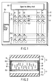
- FIG. 1 shows a planar structure of the LCD panel
- FIG. 2 shows a cross-sectional structure of pixels of the LCD panel.
- the LCD panel operates in a multi-domain VAN mode.
- the LCD panel comprises light-transmissive electrode substrates 11 and 12, and a liquid crystal layer 13 containing a nematic liquid crystal material held between the electrode substrates 11 and 12.
- the electrode substrate 11 comprises a plurality of pixel electrodes EL1 arrayed substantially in a matrix form; a plurality of scanning lines Y (Y1 to Ym) disposed along rows of the pixel electrodes EL1; a plurality of signal lines X (X1 to Xn) disposed along columns of the pixel electrodes EL1; a plurality of switching elements SW disposed near intersections of the scanning lines Y and signal lines X; a scanning line driving circuit YD for driving the scanning lines Y; and a signal line driving circuit XD for driving the signal lines X.
- the pixel electrodes EL1 are formed on an insulating substrate G1 shown in FIG.
- the switching elements SW are formed of amorphous-silicon or polysilicon thin-film transistors.
- the scanning line driving circuit YD and signal line driving circuit XD are formed of, e.g. polysilicon thin-film transistors or Si peripheral circuit. Each switching element SW is driven via a corresponding scanning line Y to electrically connect a corresponding signal line X to a corresponding pixel electrode EL1.
- the scanning lines Y, signal lines X, switching elements SW, scanning line driving circuit YD and signal line driving circuit YD are disposed on the insulating substrate G1.
- the electrode substrate 12 includes a color filter 15 formed on an insulating substrate G2; a plurality of counter electrodes EL2 formed on the color filter 15 and opposed to the pixel electrodes EL1; and an alignment film 16 which covers the counter electrodes EL2 and aligns liquid crystal molecules of the liquid crystal layer 13 substantially vertical to the electrode substrate 12 plane in a voltage non-application state.
- the color filter 15 includes three color layers of red (R), green (G) and blue (B) formed in pixel regions defined by the electrodes EL1 and EL2, and shield layers formed around the pixel regions defined by the electrodes EL1 and EL2.
- the insulating substrate G1, G2 be formed of such a transparent material as glass, polycarbonate, or a cycloolefin resin, and has low hygroscopicity, thermal resistance, low birefringence, and high dimensional stability.
- the electrode substrates G1 and G2 and liquid crystal layer 13 are integrated by means of a peripheral sealing member surrounding the liquid crystal layer 13 between the electrode substrates 11 and 12.
- the cell thickness of the liquid crystal layer 13 is kept substantially constant by columnar spacers SP which are formed in contact with the electrode substrates 11 and 12 at a central area of the pixel region and an outside area of the pixel region. It is preferable that a pre-tilt angle of liquid crystal molecules, which is provided by the alignment film 14, 16, be 90°.
- the LCD panel further comprises polarization plates PL1 and PL2 covering those surfaces of the electrode substrates 11 and 12, which are located opposite to the liquid crystal layer 13.
- the polarization plates PL1 and PL2 are affixed to the electrode substrates G1 and G2 in such orientations that their polarization axes are set in a cross-Nicol.
- the pixel electrodes EL1 and counter electrodes EL2 are, as shown in FIG. 3, circular electrodes for applying an electric field to the liquid crystal layer 13 to control orientation of liquid crystal molecules serving as a pixel of a circular form defined by these circular electrodes.
- the pixel electrodes EL1 and counter electrodes EL2 are arrayed substantially in a matrix form. In fact, however, these electrodes are slightly displaced to eliminate useless regions among the pixels, as shown in FIG. 3.
- Each of the pixel electrodes EL1 is formed of light-shielding electrode lines CM1 which are arranged radially in the pixel region, as shown in FIG. 4.
- Each of the counter electrodes EL2 is formed of light-shielding electrode lines CM2 which are arranged concentrically about the center of the pixel region, as shown in FIG. 5.
- the light-shielding electrode lines CM1 are connected to a bridge fine line BR disposed, e.g. along periphery of the pixel region.
- the light-shielding electrode lines CM2 are connected to a cruciform bridge fine lines BR disposed, e.g. to extend vertically and horizontally and intersect at the center of the pixel region.
- the light-shielding electrode lines CM1 and CM2 are opposed to each other as shown in FIG.
- the electrode lines CM1 and CM2 are formed of the light-shielding material in order to prevent the light leak from the disclination lines.
- the radius of each of the electrodes EL1 and EL2 is set at, e.g. 60 ⁇ m, and the line widths of the electrode lines CM1 and CM2 are set at 2 ⁇ m and 3 ⁇ m, respectively.
- the precision of a stepper for forming electrodes is about 1.5 ⁇ m in the state of the art.
- the precision in alignment for attaching the electrode substrates 11 and 12 is about 2 ⁇ m in the state of the art. If the precision of the stepper and the precision in alignment with these values are available, the domains DM can be obtained, as shown in FIG. 6, by precisely dividing the liquid crystal layer 13 at the intervals of about 10 ⁇ m for each pixel.
- each electrode EL1, EL2 was set at 60 ⁇ m, as mentioned above.
- the radial electrode lines CM1 were patterned with a line width of 2 ⁇ m so as to equally divide the electrode EL1 into 16 portions in its circumferential direction.
- the concentric electrode lines CM2 were patterned with a line width of 3 ⁇ m so as to divide the electrode EL2 at radial points of 10 ⁇ m, 20 ⁇ m, 30 ⁇ m, 40 ⁇ m, 50 ⁇ m and 60 ⁇ m from the center of the electrode EL2.
- the number of domains was set at 80.
- Each of the alignment films 14 and 16 was formed by vertical alignment treatment of a full-coated silane coupling material.
- FIG. 7 shows the voltage-to-transmittance characteristic of the actually manufactured LCD panel.
- the transmittance gradually rises with a threshold point of about 2V, and the contrast ratio is 210:1.
- a voltage was applied between the pixel electrode EL1 and counter electrode EL2, and the liquid crystal alignment was observed by a polarization microscope. It was confirmed that there was a multi-domain structure wherein the liquid crystal alignment differs between the domains of the pixel region partitioned by the radial electrode lines CM1 and concentric electrode lines CM2.
- FIG. 8 shows the viewing angle characteristic of the LCD panel.
- the viewing angle characteristic is measurement results obtained by applying voltages for attaining transmittances of 100%, 80%, 60%, 40%, 20% and 0% in a front view. Although the pixel was divided in units of 22.5° in the circumferential direction, the measurement results show that the variation in transmittance was substantially symmetric in all viewing angles.
- an electric field is applied to the liquid crystal layer 13 from the radial light-shielding electrode lines CM1 and concentric light-shielding electrode lines CM2.
- the liquid crystal layer 13 is divided into domains DM between which liquid crystal molecules are set in different tilt directions.
- the plural domains DM are made symmetric with respect to the center of the electrodes EL1 and EL2, and thus the unevenness in the viewing angle characteristic can be remedied.
- the domain size is gradually varied in the radial direction outward from the center of the electrodes EL1 and EL2, and thus the threshold characteristic, i.e. the point from which a change in the transmittance is initiated can be controlled.
- the threshold characteristic i.e. the point from which a change in the transmittance is initiated can be controlled.
- curves in the displayed image can be prevented from being degraded.
- the alignment films 14 and 16 are subjected to alignment treatment such that the liquid crystal molecules of the liquid crystal layer 13 are aligned substantially vertical to the planes of the electrode substrates 11 and 12 in a voltage non-application state.
- the alignment films 14 and 16 may be subjected to alignment treatment such that the liquid crystal molecules of the liquid crystal layer 13 are aligned substantially horizontal with respect to the planes of the electrode substrates 11 and 12 in a voltage non-application state.
- the pre-tilt angle of liquid crystal molecules provided by the alignment films 14 and 16 be 0°.
- the pixel electrodes EL1 as well as the scanning line driving circuit YD, signal line driving circuit XD and switching elements SW, are provided on the electrode substrate 11, and the counter electrodes EL2 are provided on the electrode substrate 12 so as to face the pixel electrodes EL1.
- the structural relationship between the pixel electrodes EL1 and the counter electrodes EL2 may be reversed since the transmittance of the liquid crystal layer 13 is controlled by a potential difference between the pixel electrodes EL1 and the counter electrodes EL2.
- each of the pixel electrodes EL1 is formed of concentric light-shielding electrode lines CM2, and each of the counter electrodes EL2 is formed of radial light-shielding electrode lines CM1.
Landscapes
- Physics & Mathematics (AREA)
- Nonlinear Science (AREA)
- Mathematical Physics (AREA)
- Chemical & Material Sciences (AREA)
- Crystallography & Structural Chemistry (AREA)
- General Physics & Mathematics (AREA)
- Optics & Photonics (AREA)
- Geometry (AREA)
- Liquid Crystal (AREA)
Applications Claiming Priority (2)
| Application Number | Priority Date | Filing Date | Title |
|---|---|---|---|
| JP2001285342A JP3656103B2 (ja) | 2001-09-19 | 2001-09-19 | 液晶表示素子 |
| JP2001285342 | 2001-09-19 |
Publications (2)
| Publication Number | Publication Date |
|---|---|
| EP1296175A2 true EP1296175A2 (de) | 2003-03-26 |
| EP1296175A3 EP1296175A3 (de) | 2004-01-28 |
Family
ID=19108505
Family Applications (1)
| Application Number | Title | Priority Date | Filing Date |
|---|---|---|---|
| EP02020580A Withdrawn EP1296175A3 (de) | 2001-09-19 | 2002-09-17 | Flüssigkristallanzeige |
Country Status (4)
| Country | Link |
|---|---|
| US (1) | US6894752B2 (de) |
| EP (1) | EP1296175A3 (de) |
| JP (1) | JP3656103B2 (de) |
| KR (1) | KR100474608B1 (de) |
Families Citing this family (20)
| Publication number | Priority date | Publication date | Assignee | Title |
|---|---|---|---|---|
| JP2004177788A (ja) * | 2002-11-28 | 2004-06-24 | Hitachi Displays Ltd | 液晶表示装置 |
| US7202928B2 (en) * | 2003-10-16 | 2007-04-10 | Lg. Philips Lcd Co., Ltd | Array substrate for in-plane switching mode liquid crystal display device and method of fabricating the same |
| KR100568959B1 (ko) * | 2003-12-11 | 2006-04-07 | 엘지.필립스 엘시디 주식회사 | 액정표시장치의 액정셀 공정 |
| KR100564218B1 (ko) * | 2003-12-11 | 2006-03-28 | 엘지.필립스 엘시디 주식회사 | 횡전계형 액정표시장치용 기판 및 그 제조 방법 |
| KR100565948B1 (ko) * | 2003-12-11 | 2006-03-30 | 엘지.필립스 엘시디 주식회사 | 횡전계형 액정표시장치의 액정셀 공정 |
| KR100643039B1 (ko) * | 2003-12-11 | 2006-11-10 | 엘지.필립스 엘시디 주식회사 | 횡전계형 액정표시장치 |
| KR100564219B1 (ko) * | 2003-12-11 | 2006-03-28 | 엘지.필립스 엘시디 주식회사 | 횡전계형 액정표시장치용 어레이 기판 |
| US7227607B2 (en) * | 2003-12-11 | 2007-06-05 | Lg.Philips Lcd Co., Ltd | Array substrate for in-plane switching mode liquid crystal display device and method of fabricating the same |
| US7304709B2 (en) * | 2003-12-12 | 2007-12-04 | Lg. Philips Lcd Co., Ltd. | Fringe field switching mode liquid crystal display device and method of fabricating the same |
| KR100565148B1 (ko) * | 2003-12-16 | 2006-03-30 | 엘지.필립스 엘시디 주식회사 | 액정표시장치 및 그 제조방법 |
| KR20050060594A (ko) * | 2003-12-17 | 2005-06-22 | 엘지.필립스 엘시디 주식회사 | 액정표시장치 |
| KR20050067682A (ko) * | 2003-12-29 | 2005-07-05 | 엘지.필립스 엘시디 주식회사 | 횡전계형 액정표시장치 및 그 구동방법 |
| KR101041057B1 (ko) * | 2004-01-09 | 2011-06-13 | 삼성전자주식회사 | 표시장치 |
| US7466385B2 (en) * | 2004-12-23 | 2008-12-16 | University Of Central Florida Research Foundation, Inc. | Vertical alignment liquid crystal displays with high transmittance and wide view angle |
| US8928845B2 (en) * | 2005-04-22 | 2015-01-06 | Citizen Holdings Co., Ltd. | Liquid crystal optical element, optical device, and aperture control method |
| KR100668140B1 (ko) * | 2005-11-11 | 2007-01-16 | 비오이 하이디스 테크놀로지 주식회사 | 수직 배향 모드 액정표시장치 |
| KR101245126B1 (ko) * | 2006-02-07 | 2013-03-25 | 삼성디스플레이 주식회사 | 액정표시패널 및 이를 갖는 액정표시장치 |
| CN101957692B (zh) * | 2009-07-17 | 2013-08-21 | 鸿富锦精密工业(深圳)有限公司 | 触控装置及手写输入系统 |
| TWI450139B (zh) * | 2009-08-11 | 2014-08-21 | Hon Hai Prec Ind Co Ltd | 觸控裝置及手寫輸入系統 |
| JP5846770B2 (ja) * | 2011-06-21 | 2016-01-20 | 日本放送協会 | 液晶表示パネルの電極構造およびホログラム記録装置 |
Family Cites Families (20)
| Publication number | Priority date | Publication date | Assignee | Title |
|---|---|---|---|---|
| JPS6319880A (ja) | 1986-07-14 | 1988-01-27 | Hitachi Ltd | 太陽電池用基板 |
| DE3856483T2 (de) * | 1987-03-18 | 2002-04-18 | Kabushiki Kaisha Toshiba, Kawasaki | Verfahren zur Herstellung von Dünnschichten |
| US5028566A (en) * | 1987-04-10 | 1991-07-02 | Air Products And Chemicals, Inc. | Method of forming silicon dioxide glass films |
| CA2017719C (en) * | 1990-05-29 | 1999-01-19 | Zarlink Semiconductor Inc. | Moisture-free sog process |
| US5309264A (en) * | 1992-04-30 | 1994-05-03 | International Business Machines Corporation | Liquid crystal displays having multi-domain cells |
| JPH06324337A (ja) | 1993-03-15 | 1994-11-25 | Toshiba Corp | 液晶表示装置 |
| JP3529434B2 (ja) | 1993-07-27 | 2004-05-24 | 株式会社東芝 | 液晶表示素子 |
| JPH0921913A (ja) * | 1995-07-05 | 1997-01-21 | Sharp Corp | 軸対称偏光板及びその製造方法,並びに液晶表示装置 |
| TW354833B (en) | 1995-08-23 | 1999-03-21 | United Microelectronics Corp | Liquid crystal display with improved viewing angle and method of producing the same |
| US5719085A (en) * | 1995-09-29 | 1998-02-17 | Intel Corporation | Shallow trench isolation technique |
| US5610743A (en) * | 1995-10-30 | 1997-03-11 | United Microelectronics Corporation | Liquid crystal display including concentric shapes and radial spokes which has an improved viewing angle |
| KR100209365B1 (ko) * | 1995-11-01 | 1999-07-15 | 김영환 | 에스.오.아이 반도체 웨이퍼의 제조방법 |
| JPH09304757A (ja) | 1996-03-11 | 1997-11-28 | Sharp Corp | 液晶表示素子及びその製造方法 |
| TW589504B (en) | 1997-06-12 | 2004-06-01 | Sharp Kk | Liquid crystal display device |
| US5883006A (en) * | 1997-12-12 | 1999-03-16 | Kabushiki Kaisha Toshiba | Method for making a semiconductor device using a flowable oxide film |
| US6030881A (en) * | 1998-05-05 | 2000-02-29 | Novellus Systems, Inc. | High throughput chemical vapor deposition process capable of filling high aspect ratio structures |
| KR100354904B1 (ko) * | 1998-05-19 | 2002-12-26 | 삼성전자 주식회사 | 광시야각액정표시장치 |
| KR100286978B1 (ko) * | 1999-03-04 | 2001-04-16 | 윤종용 | 반사형 액정표시장치 및 그 제조방법 |
| KR100601173B1 (ko) * | 1999-06-30 | 2006-07-13 | 삼성전자주식회사 | 액정 표시 장치 |
| JP3941437B2 (ja) | 2001-08-31 | 2007-07-04 | セイコーエプソン株式会社 | 液晶表示装置およびその製造方法ならびに電子機器 |
-
2001
- 2001-09-19 JP JP2001285342A patent/JP3656103B2/ja not_active Expired - Lifetime
-
2002
- 2002-09-17 EP EP02020580A patent/EP1296175A3/de not_active Withdrawn
- 2002-09-18 KR KR10-2002-0056873A patent/KR100474608B1/ko not_active Expired - Fee Related
- 2002-09-18 US US10/245,756 patent/US6894752B2/en not_active Expired - Fee Related
Also Published As
| Publication number | Publication date |
|---|---|
| EP1296175A3 (de) | 2004-01-28 |
| US6894752B2 (en) | 2005-05-17 |
| US20030053020A1 (en) | 2003-03-20 |
| KR100474608B1 (ko) | 2005-03-10 |
| JP2003091009A (ja) | 2003-03-28 |
| JP3656103B2 (ja) | 2005-06-08 |
| KR20030025206A (ko) | 2003-03-28 |
Similar Documents
| Publication | Publication Date | Title |
|---|---|---|
| US6894752B2 (en) | Liquid crystal display device | |
| KR100209531B1 (ko) | 액정표시장치 | |
| US8094282B1 (en) | Method of fabricating a liquid crystal display device having image-displaying and viewing angle-adjusting sub pixels and method of driving the same | |
| JP3066255B2 (ja) | 液晶表示装置 | |
| JP3234357B2 (ja) | 液晶表示装置 | |
| JPH06160878A (ja) | 液晶表示装置 | |
| US7113240B2 (en) | Liquid crystal display device having insulating patterns with width larger than gap in between | |
| US20010043301A1 (en) | Structure of a multi-domain wide viewing angle liquid crystal display | |
| US6940571B2 (en) | Liquid crystal display device | |
| US6476896B1 (en) | Structure of a multi-domain wide viewing angle liquid crystal display | |
| US7259819B2 (en) | Liquid crystal display device with a bridge wiring member with an electric field weaker than that created in minute domains above the pixel electrode | |
| US7423715B2 (en) | Liquid crystal display device with retardation layer | |
| US20070040974A1 (en) | Liquid crystal display panel | |
| CN1708724A (zh) | 多区域垂直排列液晶显示器 | |
| JP2004037850A (ja) | 液晶表示装置 | |
| US20080225212A1 (en) | Pixel designs for multi-domain vertical alignment liquid crystal display | |
| JP4127623B2 (ja) | 液晶表示装置 | |
| WO2004015487A1 (en) | A panel and a liquid crystal display including the panel | |
| JP2002098967A (ja) | 液晶表示装置 | |
| JPH09230364A (ja) | 液晶表示装置 | |
| KR101108387B1 (ko) | 티엔 모드 액정표시장치 및 그 제조방법 | |
| JP2001255524A (ja) | 液晶表示素子 | |
| JP3441999B2 (ja) | 液晶表示装置 | |
| JP2005316331A (ja) | 液晶表示装置 | |
| JP2007163590A (ja) | 液晶表示装置 |
Legal Events
| Date | Code | Title | Description |
|---|---|---|---|
| PUAI | Public reference made under article 153(3) epc to a published international application that has entered the european phase |
Free format text: ORIGINAL CODE: 0009012 |
|
| 17P | Request for examination filed |
Effective date: 20020917 |
|
| AK | Designated contracting states |
Kind code of ref document: A2 Designated state(s): AT BE BG CH CY CZ DE DK EE ES FI FR GB GR IE IT LI LU MC NL PT SE SK TR Designated state(s): AT BE BG CH CY CZ DE DK EE ES FI FR GB GR IE IT LI LU MC NL PT SE SK TR |
|
| AX | Request for extension of the european patent |
Extension state: AL LT LV MK RO SI |
|
| PUAL | Search report despatched |
Free format text: ORIGINAL CODE: 0009013 |
|
| AK | Designated contracting states |
Kind code of ref document: A3 Designated state(s): AT BE BG CH CY CZ DE DK EE ES FI FR GB GR IE IT LI LU MC NL PT SE SK TR |
|
| AX | Request for extension of the european patent |
Extension state: AL LT LV MK RO SI |
|
| RIC1 | Information provided on ipc code assigned before grant |
Ipc: 7G 02F 1/139 B Ipc: 7G 02F 1/1368 B Ipc: 7G 02F 1/1343 A |
|
| 17Q | First examination report despatched |
Effective date: 20040720 |
|
| AKX | Designation fees paid |
Designated state(s): AT DE FR GB |
|
| GRAP | Despatch of communication of intention to grant a patent |
Free format text: ORIGINAL CODE: EPIDOSNIGR1 |
|
| STAA | Information on the status of an ep patent application or granted ep patent |
Free format text: STATUS: THE APPLICATION IS DEEMED TO BE WITHDRAWN |
|
| 18D | Application deemed to be withdrawn |
Effective date: 20050921 |