EP1298968B1 - Metall bekleidete keramische Schaltungsplatte - Google Patents
Metall bekleidete keramische Schaltungsplatte Download PDFInfo
- Publication number
- EP1298968B1 EP1298968B1 EP02021755A EP02021755A EP1298968B1 EP 1298968 B1 EP1298968 B1 EP 1298968B1 EP 02021755 A EP02021755 A EP 02021755A EP 02021755 A EP02021755 A EP 02021755A EP 1298968 B1 EP1298968 B1 EP 1298968B1
- Authority
- EP
- European Patent Office
- Prior art keywords
- metal
- plate
- circuit board
- ceramic
- ceramic substrate
- Prior art date
- Legal status (The legal status is an assumption and is not a legal conclusion. Google has not performed a legal analysis and makes no representation as to the accuracy of the status listed.)
- Expired - Lifetime
Links
Images


Classifications
-
- H—ELECTRICITY
- H05—ELECTRIC TECHNIQUES NOT OTHERWISE PROVIDED FOR
- H05K—PRINTED CIRCUITS; CASINGS OR CONSTRUCTIONAL DETAILS OF ELECTRIC APPARATUS; MANUFACTURE OF ASSEMBLAGES OF ELECTRICAL COMPONENTS
- H05K3/00—Apparatus or processes for manufacturing printed circuits
- H05K3/38—Improvement of the adhesion between the insulating substrate and the metal
-
- C—CHEMISTRY; METALLURGY
- C04—CEMENTS; CONCRETE; ARTIFICIAL STONE; CERAMICS; REFRACTORIES
- C04B—LIME, MAGNESIA; SLAG; CEMENTS; COMPOSITIONS THEREOF, e.g. MORTARS, CONCRETE OR LIKE BUILDING MATERIALS; ARTIFICIAL STONE; CERAMICS; REFRACTORIES; TREATMENT OF NATURAL STONE
- C04B37/00—Joining burned ceramic articles with other burned ceramic articles or other articles by heating
- C04B37/02—Joining burned ceramic articles with other burned ceramic articles or other articles by heating with metallic articles
- C04B37/021—Joining burned ceramic articles with other burned ceramic articles or other articles by heating with metallic articles in a direct manner, e.g. direct copper bonding [DCB]
-
- C—CHEMISTRY; METALLURGY
- C04—CEMENTS; CONCRETE; ARTIFICIAL STONE; CERAMICS; REFRACTORIES
- C04B—LIME, MAGNESIA; SLAG; CEMENTS; COMPOSITIONS THEREOF, e.g. MORTARS, CONCRETE OR LIKE BUILDING MATERIALS; ARTIFICIAL STONE; CERAMICS; REFRACTORIES; TREATMENT OF NATURAL STONE
- C04B37/00—Joining burned ceramic articles with other burned ceramic articles or other articles by heating
- C04B37/02—Joining burned ceramic articles with other burned ceramic articles or other articles by heating with metallic articles
- C04B37/023—Joining burned ceramic articles with other burned ceramic articles or other articles by heating with metallic articles characterised by the interlayer used
- C04B37/026—Joining burned ceramic articles with other burned ceramic articles or other articles by heating with metallic articles characterised by the interlayer used consisting of metals or metal salts
-
- H—ELECTRICITY
- H05—ELECTRIC TECHNIQUES NOT OTHERWISE PROVIDED FOR
- H05K—PRINTED CIRCUITS; CASINGS OR CONSTRUCTIONAL DETAILS OF ELECTRIC APPARATUS; MANUFACTURE OF ASSEMBLAGES OF ELECTRICAL COMPONENTS
- H05K3/00—Apparatus or processes for manufacturing printed circuits
- H05K3/02—Apparatus or processes for manufacturing printed circuits in which the conductive material is applied to the surface of the insulating support and is thereafter removed from such areas of the surface which are not intended for current conducting or shielding
- H05K3/06—Apparatus or processes for manufacturing printed circuits in which the conductive material is applied to the surface of the insulating support and is thereafter removed from such areas of the surface which are not intended for current conducting or shielding the conductive material being removed chemically or electrolytically, e.g. by photo-etch process
-
- H—ELECTRICITY
- H10—SEMICONDUCTOR DEVICES; ELECTRIC SOLID-STATE DEVICES NOT OTHERWISE PROVIDED FOR
- H10W—GENERIC PACKAGES, INTERCONNECTIONS, CONNECTORS OR OTHER CONSTRUCTIONAL DETAILS OF DEVICES COVERED BY CLASS H10
- H10W40/00—Arrangements for thermal protection or thermal control
- H10W40/20—Arrangements for cooling
- H10W40/25—Arrangements for cooling characterised by their materials
- H10W40/255—Arrangements for cooling characterised by their materials having a laminate or multilayered structure, e.g. direct bond copper [DBC] ceramic substrates
-
- C—CHEMISTRY; METALLURGY
- C04—CEMENTS; CONCRETE; ARTIFICIAL STONE; CERAMICS; REFRACTORIES
- C04B—LIME, MAGNESIA; SLAG; CEMENTS; COMPOSITIONS THEREOF, e.g. MORTARS, CONCRETE OR LIKE BUILDING MATERIALS; ARTIFICIAL STONE; CERAMICS; REFRACTORIES; TREATMENT OF NATURAL STONE
- C04B2237/00—Aspects relating to ceramic laminates or to joining of ceramic articles with other articles by heating
- C04B2237/02—Aspects relating to interlayers, e.g. used to join ceramic articles with other articles by heating
- C04B2237/12—Metallic interlayers
- C04B2237/121—Metallic interlayers based on aluminium
-
- C—CHEMISTRY; METALLURGY
- C04—CEMENTS; CONCRETE; ARTIFICIAL STONE; CERAMICS; REFRACTORIES
- C04B—LIME, MAGNESIA; SLAG; CEMENTS; COMPOSITIONS THEREOF, e.g. MORTARS, CONCRETE OR LIKE BUILDING MATERIALS; ARTIFICIAL STONE; CERAMICS; REFRACTORIES; TREATMENT OF NATURAL STONE
- C04B2237/00—Aspects relating to ceramic laminates or to joining of ceramic articles with other articles by heating
- C04B2237/02—Aspects relating to interlayers, e.g. used to join ceramic articles with other articles by heating
- C04B2237/12—Metallic interlayers
- C04B2237/125—Metallic interlayers based on noble metals, e.g. silver
-
- C—CHEMISTRY; METALLURGY
- C04—CEMENTS; CONCRETE; ARTIFICIAL STONE; CERAMICS; REFRACTORIES
- C04B—LIME, MAGNESIA; SLAG; CEMENTS; COMPOSITIONS THEREOF, e.g. MORTARS, CONCRETE OR LIKE BUILDING MATERIALS; ARTIFICIAL STONE; CERAMICS; REFRACTORIES; TREATMENT OF NATURAL STONE
- C04B2237/00—Aspects relating to ceramic laminates or to joining of ceramic articles with other articles by heating
- C04B2237/02—Aspects relating to interlayers, e.g. used to join ceramic articles with other articles by heating
- C04B2237/12—Metallic interlayers
- C04B2237/126—Metallic interlayers wherein the active component for bonding is not the largest fraction of the interlayer
- C04B2237/127—The active component for bonding being a refractory metal
-
- C—CHEMISTRY; METALLURGY
- C04—CEMENTS; CONCRETE; ARTIFICIAL STONE; CERAMICS; REFRACTORIES
- C04B—LIME, MAGNESIA; SLAG; CEMENTS; COMPOSITIONS THEREOF, e.g. MORTARS, CONCRETE OR LIKE BUILDING MATERIALS; ARTIFICIAL STONE; CERAMICS; REFRACTORIES; TREATMENT OF NATURAL STONE
- C04B2237/00—Aspects relating to ceramic laminates or to joining of ceramic articles with other articles by heating
- C04B2237/02—Aspects relating to interlayers, e.g. used to join ceramic articles with other articles by heating
- C04B2237/12—Metallic interlayers
- C04B2237/126—Metallic interlayers wherein the active component for bonding is not the largest fraction of the interlayer
- C04B2237/128—The active component for bonding being silicon
-
- C—CHEMISTRY; METALLURGY
- C04—CEMENTS; CONCRETE; ARTIFICIAL STONE; CERAMICS; REFRACTORIES
- C04B—LIME, MAGNESIA; SLAG; CEMENTS; COMPOSITIONS THEREOF, e.g. MORTARS, CONCRETE OR LIKE BUILDING MATERIALS; ARTIFICIAL STONE; CERAMICS; REFRACTORIES; TREATMENT OF NATURAL STONE
- C04B2237/00—Aspects relating to ceramic laminates or to joining of ceramic articles with other articles by heating
- C04B2237/30—Composition of layers of ceramic laminates or of ceramic or metallic articles to be joined by heating, e.g. Si substrates
- C04B2237/32—Ceramic
- C04B2237/36—Non-oxidic
- C04B2237/366—Aluminium nitride
-
- C—CHEMISTRY; METALLURGY
- C04—CEMENTS; CONCRETE; ARTIFICIAL STONE; CERAMICS; REFRACTORIES
- C04B—LIME, MAGNESIA; SLAG; CEMENTS; COMPOSITIONS THEREOF, e.g. MORTARS, CONCRETE OR LIKE BUILDING MATERIALS; ARTIFICIAL STONE; CERAMICS; REFRACTORIES; TREATMENT OF NATURAL STONE
- C04B2237/00—Aspects relating to ceramic laminates or to joining of ceramic articles with other articles by heating
- C04B2237/30—Composition of layers of ceramic laminates or of ceramic or metallic articles to be joined by heating, e.g. Si substrates
- C04B2237/40—Metallic
- C04B2237/402—Aluminium
-
- C—CHEMISTRY; METALLURGY
- C04—CEMENTS; CONCRETE; ARTIFICIAL STONE; CERAMICS; REFRACTORIES
- C04B—LIME, MAGNESIA; SLAG; CEMENTS; COMPOSITIONS THEREOF, e.g. MORTARS, CONCRETE OR LIKE BUILDING MATERIALS; ARTIFICIAL STONE; CERAMICS; REFRACTORIES; TREATMENT OF NATURAL STONE
- C04B2237/00—Aspects relating to ceramic laminates or to joining of ceramic articles with other articles by heating
- C04B2237/30—Composition of layers of ceramic laminates or of ceramic or metallic articles to be joined by heating, e.g. Si substrates
- C04B2237/40—Metallic
- C04B2237/407—Copper
-
- C—CHEMISTRY; METALLURGY
- C04—CEMENTS; CONCRETE; ARTIFICIAL STONE; CERAMICS; REFRACTORIES
- C04B—LIME, MAGNESIA; SLAG; CEMENTS; COMPOSITIONS THEREOF, e.g. MORTARS, CONCRETE OR LIKE BUILDING MATERIALS; ARTIFICIAL STONE; CERAMICS; REFRACTORIES; TREATMENT OF NATURAL STONE
- C04B2237/00—Aspects relating to ceramic laminates or to joining of ceramic articles with other articles by heating
- C04B2237/50—Processing aspects relating to ceramic laminates or to the joining of ceramic articles with other articles by heating
- C04B2237/70—Forming laminates or joined articles comprising layers of a specific, unusual thickness
- C04B2237/706—Forming laminates or joined articles comprising layers of a specific, unusual thickness of one or more of the metallic layers or articles
-
- H—ELECTRICITY
- H05—ELECTRIC TECHNIQUES NOT OTHERWISE PROVIDED FOR
- H05K—PRINTED CIRCUITS; CASINGS OR CONSTRUCTIONAL DETAILS OF ELECTRIC APPARATUS; MANUFACTURE OF ASSEMBLAGES OF ELECTRICAL COMPONENTS
- H05K1/00—Printed circuits
- H05K1/02—Details
- H05K1/03—Use of materials for the substrate
- H05K1/0306—Inorganic insulating substrates, e.g. ceramic, glass
-
- H—ELECTRICITY
- H05—ELECTRIC TECHNIQUES NOT OTHERWISE PROVIDED FOR
- H05K—PRINTED CIRCUITS; CASINGS OR CONSTRUCTIONAL DETAILS OF ELECTRIC APPARATUS; MANUFACTURE OF ASSEMBLAGES OF ELECTRICAL COMPONENTS
- H05K2201/00—Indexing scheme relating to printed circuits covered by H05K1/00
- H05K2201/03—Conductive materials
- H05K2201/0332—Structure of the conductor
- H05K2201/0335—Layered conductors or foils
- H05K2201/0355—Metal foils
-
- H—ELECTRICITY
- H05—ELECTRIC TECHNIQUES NOT OTHERWISE PROVIDED FOR
- H05K—PRINTED CIRCUITS; CASINGS OR CONSTRUCTIONAL DETAILS OF ELECTRIC APPARATUS; MANUFACTURE OF ASSEMBLAGES OF ELECTRICAL COMPONENTS
- H05K2201/00—Indexing scheme relating to printed circuits covered by H05K1/00
- H05K2201/09—Shape and layout
- H05K2201/09209—Shape and layout details of conductors
- H05K2201/09654—Shape and layout details of conductors covering at least two types of conductors provided for in H05K2201/09218 - H05K2201/095
- H05K2201/098—Special shape of the cross-section of conductors, e.g. very thick plated conductors
-
- H—ELECTRICITY
- H05—ELECTRIC TECHNIQUES NOT OTHERWISE PROVIDED FOR
- H05K—PRINTED CIRCUITS; CASINGS OR CONSTRUCTIONAL DETAILS OF ELECTRIC APPARATUS; MANUFACTURE OF ASSEMBLAGES OF ELECTRICAL COMPONENTS
- H05K3/00—Apparatus or processes for manufacturing printed circuits
- H05K3/02—Apparatus or processes for manufacturing printed circuits in which the conductive material is applied to the surface of the insulating support and is thereafter removed from such areas of the surface which are not intended for current conducting or shielding
- H05K3/06—Apparatus or processes for manufacturing printed circuits in which the conductive material is applied to the surface of the insulating support and is thereafter removed from such areas of the surface which are not intended for current conducting or shielding the conductive material being removed chemically or electrolytically, e.g. by photo-etch process
- H05K3/067—Etchants
-
- H—ELECTRICITY
- H05—ELECTRIC TECHNIQUES NOT OTHERWISE PROVIDED FOR
- H05K—PRINTED CIRCUITS; CASINGS OR CONSTRUCTIONAL DETAILS OF ELECTRIC APPARATUS; MANUFACTURE OF ASSEMBLAGES OF ELECTRICAL COMPONENTS
- H05K3/00—Apparatus or processes for manufacturing printed circuits
- H05K3/22—Secondary treatment of printed circuits
- H05K3/24—Reinforcing of the conductive pattern
- H05K3/244—Finish plating of conductors, especially of copper conductors, e.g. for pads or lands
-
- Y—GENERAL TAGGING OF NEW TECHNOLOGICAL DEVELOPMENTS; GENERAL TAGGING OF CROSS-SECTIONAL TECHNOLOGIES SPANNING OVER SEVERAL SECTIONS OF THE IPC; TECHNICAL SUBJECTS COVERED BY FORMER USPC CROSS-REFERENCE ART COLLECTIONS [XRACs] AND DIGESTS
- Y10—TECHNICAL SUBJECTS COVERED BY FORMER USPC
- Y10T—TECHNICAL SUBJECTS COVERED BY FORMER US CLASSIFICATION
- Y10T428/00—Stock material or miscellaneous articles
- Y10T428/12—All metal or with adjacent metals
- Y10T428/12493—Composite; i.e., plural, adjacent, spatially distinct metal components [e.g., layers, joint, etc.]
- Y10T428/12535—Composite; i.e., plural, adjacent, spatially distinct metal components [e.g., layers, joint, etc.] with additional, spatially distinct nonmetal component
-
- Y—GENERAL TAGGING OF NEW TECHNOLOGICAL DEVELOPMENTS; GENERAL TAGGING OF CROSS-SECTIONAL TECHNOLOGIES SPANNING OVER SEVERAL SECTIONS OF THE IPC; TECHNICAL SUBJECTS COVERED BY FORMER USPC CROSS-REFERENCE ART COLLECTIONS [XRACs] AND DIGESTS
- Y10—TECHNICAL SUBJECTS COVERED BY FORMER USPC
- Y10T—TECHNICAL SUBJECTS COVERED BY FORMER US CLASSIFICATION
- Y10T428/00—Stock material or miscellaneous articles
- Y10T428/12—All metal or with adjacent metals
- Y10T428/12493—Composite; i.e., plural, adjacent, spatially distinct metal components [e.g., layers, joint, etc.]
- Y10T428/12535—Composite; i.e., plural, adjacent, spatially distinct metal components [e.g., layers, joint, etc.] with additional, spatially distinct nonmetal component
- Y10T428/12576—Boride, carbide or nitride component
-
- Y—GENERAL TAGGING OF NEW TECHNOLOGICAL DEVELOPMENTS; GENERAL TAGGING OF CROSS-SECTIONAL TECHNOLOGIES SPANNING OVER SEVERAL SECTIONS OF THE IPC; TECHNICAL SUBJECTS COVERED BY FORMER USPC CROSS-REFERENCE ART COLLECTIONS [XRACs] AND DIGESTS
- Y10—TECHNICAL SUBJECTS COVERED BY FORMER USPC
- Y10T—TECHNICAL SUBJECTS COVERED BY FORMER US CLASSIFICATION
- Y10T428/00—Stock material or miscellaneous articles
- Y10T428/24—Structurally defined web or sheet [e.g., overall dimension, etc.]
- Y10T428/24802—Discontinuous or differential coating, impregnation or bond [e.g., artwork, printing, retouched photograph, etc.]
- Y10T428/24917—Discontinuous or differential coating, impregnation or bond [e.g., artwork, printing, retouched photograph, etc.] including metal layer
-
- Y—GENERAL TAGGING OF NEW TECHNOLOGICAL DEVELOPMENTS; GENERAL TAGGING OF CROSS-SECTIONAL TECHNOLOGIES SPANNING OVER SEVERAL SECTIONS OF THE IPC; TECHNICAL SUBJECTS COVERED BY FORMER USPC CROSS-REFERENCE ART COLLECTIONS [XRACs] AND DIGESTS
- Y10—TECHNICAL SUBJECTS COVERED BY FORMER USPC
- Y10T—TECHNICAL SUBJECTS COVERED BY FORMER US CLASSIFICATION
- Y10T428/00—Stock material or miscellaneous articles
- Y10T428/24—Structurally defined web or sheet [e.g., overall dimension, etc.]
- Y10T428/24802—Discontinuous or differential coating, impregnation or bond [e.g., artwork, printing, retouched photograph, etc.]
- Y10T428/24926—Discontinuous or differential coating, impregnation or bond [e.g., artwork, printing, retouched photograph, etc.] including ceramic, glass, porcelain or quartz layer
Definitions
- the present invention generally relates to a metal/ceramic circuit board having a ceramic substrate and a metal circuit plate which is formed on the ceramic substrate directly or via a brazing filler metal or the like. More specifically, the invention relates to a metal/ceramic circuit board on which parts, such as semiconductor parts, are mounted and which is used for a power module or a Peltier element module.
- a metal plate and a ceramic substrate are first bonded to each other.
- the direct bonding method for arranging a copper plate on a ceramic substrate so as to allow the copper plate to directly contact the ceramic substrate and for heating the copper plate and the ceramic substrate in an inert gas to bond the ceramic substrate and the copper plate to each other.
- the brazing and soldering method for arranging a copper plate on a ceramic substrate via a brazing filler metal containing an active metal, such as Ti, Zr or Hf, and for heating them in a vacuum to bond the ceramic substrate and the copper plate to each other.
- the active metal concerns the bonding of the ceramic substrate to the metal plate, and the ceramic substrate reacts with the brazing filler metal to form a reaction product.
- EP 0 935 286 A1 discloses a copper circuit-joined board comprising at least one joining unit containing a ceramic substrate being joined to a conductor layer containing copper as a main component through an interposing layer, wherein the length and width in the planar direction of the conductor layer in the interface between the conductor layer and the interposing layer are at least 0.05 mm shorter than those in the planar direction of the interposing layer, and, wherein the outer peripheral side portion of the conductor layer in the interface between the conductor layer and the interposing layer does not extend from the outer peripheral side portion of the interposing layer.
- the created thermal stress shall be dispersed through the interposing layer in the outward of the substrate so that neither cracking nor warpage is created at the time of mounting the conductor layer on the ceramic substrate and during use.
- circuit boards for power boards the minimum distance between patterns is generally about 0.5 mm, and it is required to ensure a certain withstand voltage.
- circuit boards for Peltier elements and high frequency circuits it is required to form finer patterns. Therefore, the above described metal plate bonding method is not suitable for the production of such circuit boards, so that a metal film is formed on a ceramic substrate by plating or spattering.
- the dimensional difference between the bottom and top faces of the peripheral edge portion of a metal circuit plate is about 50 % of the thickness of the metal circuit plate.
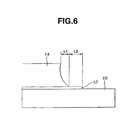
- This difference is the distance between a plane perpendicular to the principal plane of a metal plate at one end of the bottom face of the metal plate and a plane perpendicular to the principal plane of the metal date at one end of the top face of the metal plate on the same side as the one end of the bottom face of the metal plate, i.e., the length shown by L1 in FIG. 6. It is assumed that the sign of the distance is positive (+) when the area of the bottom face is greater than the area of the top face.
- L2 denotes a "brazing filler metal protruding length".
- a resin substrate such as a glass epoxy substrate
- a metal thin film having a thickness of several micrometers is formed on a ceramic substrate by spattering or plating to form a circuit
- the skirt spreading lengths are over ten micrometers and several micrometers, respectively. Such dimensional differences do not influence the formation of the circuit and precision.
- the metal plate in a substrate where a metal plate is bonded to a ceramic substrate directly or via a brazing filler metal, the metal plate usually has a relatively large thickness of about 100 to 500 ⁇ m, and the skirt spreading length of the metal circuit plate is at least in the range of from about 50 ⁇ m to about 250 ⁇ m. Such a dimensional difference can not ignore in order to form a fine circuit.
- skirt spreading length of a metal circuit plate in a conventional metal/ceramic substrate is generally in the range of from about 50 ⁇ m to about 200 ⁇ m
- a metal/ceramic circuit board wherein the skirt spreading length of a metal circuit plate is in the range of from 50 ⁇ m to 100 ⁇ m (see Japanese Patent Laid-Open No. 10-326949).
- the parts are mounted using a solder paste or the like. If the semiconductor mounting design area (the area of the top of the metal plate) is small, even if the amount of the paste slightly decreases, the possibility of producing voids increases.
- the discrepancy in mounting of these parts decreases the effective heat transfer area of parts, such as an area below a chip, in a substrate similar to a power module. Therefore, there are some cases where heat dissipation decreases to accumulate heat in the circuit to promote the deterioration of reliability. For example, if a 11 x 11 mm part is displaced by 0.1 mm in horizontal (x, y) directions in the mounting portion to protrude, respectively, the effective heat transfer area decreases by about 2 %, and if a 0.8 x 1.8 mm part is displace by 0.1 mm in horizontal (x, y) directions in the mounting portion to protrude, respectively, the effective heat transfer area decreases by about 17 %.
- the inventors have diligently studied and found that it is possible to decrease the skirt spreading length of a metal circuit board in comparison with that of a conventional metal circuit board, to increase the area of a circuit pattern, i.e., a part mounting area, to improve the reliability of mounting of parts, by studying etching conditions for the metal circuit plate.
- a metal/ceramic circuit board comprising: a ceramic substrate; and a metal circuit plate arranged on the ceramic substrate, the metal circuit plate having a thickness of 0.1 mm to 0.5 mm, and the metal circuit plate having a skirt spreading length of less than 50 ⁇ m, the skirt spreading length being a distance between a plane perpendicular to a principal plane of the metal plate at one end of a bottom face of the metal plate and a plane perpendicular to a principal plane of the metal plate at one end of a top face of the metal plate on the same side as the one end of the bottom face of the metal plate assuming that the distance is positive when the bottom face has a greater area than that of the top face, wherein a super power element is mounted on the metal/ceramic circuit board or the metal/ceramic board has a fine pattern on which a Peltier element or a high frequency circuit is mounted.
- the metal circuit plate may be bonded directly to the ceramic substrate.
- the metal circuit plate is preferably treated by nickel plating, nickel alloy plating, gold plating or preservation.
- the metal circuit plate may be bonded to the ceramic substrate via a brazing filler metal.
- the brazing filler metal is preferably made of a material selected from the group consisting of alloys and compounds containing Ag and an active metal, alloys and compounds containing Al, and mixtures thereof.
- the metal circuit plate and the brazing filler metal are preferably treated by nickel plating, nickel alloy plating, gold plating or preservation.
- the ceramic substrate is preferably formed of a material selected from the group consisting of oxides, nitrides and carbides.
- the metal circuit plate is preferably formed of a material selected from the group consisting of copper, aluminum, and alloys thereof.
- a module is assembled by using the above described metal/ceramic circuit board.
- the preferred embodiment of a metal/ceramic circuit board according to the present invention is produced by using the direct bonding method for arranging a metal plate on a ceramic substrate so as to allow the metal plate to directly contact the ceramic substrate and for heating the metal plate and the ceramic substrate in an inert gas to bond the ceramic substrate and the metal plate to each other, or by using the brazing and soldering method for arranging a metal plate on a ceramic substrate via a brazing filler metal containing an active metal, such as Ti, Zr or Hf, to heat them in a vacuum to bond the ceramic substrate and the metal plate to each other.
- an active metal such as Ti, Zr or Hf
- a method for brazing and soldering a metal plate to a ceramic substrate via Al-Si or Al-Si-Ti brazing filler metals containing Al, or a method for bonding a metal plate directly to a ceramic substrate by the molten metal bonding method may be used. These methods are preferred when the metal plate is an Al plate.
- an etching resist is applied on the surface of the metal plate in a pattern shape (or the surface of the metal plate is masked with an etching resist in a pattern shape), to etch the metal plate in a predetermined pattern.
- a method for bonding a metal plate to a ceramic substrate after forming a metal plate having a predetermined pattern shape by press working or etching may be used.
- the etching method is preferred in view of the dimensional precision or positional precision of the pattern.
- the above described methods may be chosen in view of the required precision and costs.
- a mixed solution of iron chloride or copper chloride and hydrochloric acid and aqueous hydrogen peroxide may be used.
- reactionproducts canbe ignored, so that the copper plate can be etched to form a pattern without causing problems.
- the brazing filler metal remains, so that it is required to remove the brazing filler metal with other chemicals.
- the skirt spreading length is set to be less than 50 ⁇ m by optimizing etching conditions and the design of the dimension of the mask used for etching.
- a metal plate having a predetermined pattern shape is bonded to a ceramic substrate, it is required to control the skirt spreading length in the metal plate working stage, and it is required to optimize the skirt spreading length in view of thermal expansion and contraction caused by overheating and supercooling due to bonding.
- Ni plating or Ni alloy plating is carried out if necessary.
- chip parts such as semiconductor parts, are mounted thereon by soldering or the like, to be used as a power module, a Peltier element or a high frequency circuit board.
- the weight of metal powder containing metal components was measured so that the components are 91 Ag - 7 Cu -1.5 Ti - 0.5 TiO 2 (wt%).
- To this metal powder about 10 % of an acrylic vehicle was added.
- a paste-like brazing filler metal was prepared.
- a ceramic substrate 10 was prepared (FIG. 1A), and the brazing filler metal 12 was applied on both faces of the ceramic substrate 10 by the screen printing (FIG. 1B). Then, copper plates 14 having a thickness of 0.25 mm were arranged on both side thereof, and the copper plates 14 were bonded to the ceramic substrate 10 at 835 °C in a vacuum furnace. In order to verify the thickness of the brazing filler metal 12, the sample thus bonded was cut to measure the thickness of the brazing filler metal 12. As a result, the thickness of the brazing filler metal 12 was about 20 ⁇ m.
- the ceramic substrate 10 an S grade AlN substrate produced by ATG company was used.
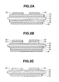
- FIGS. 2A through 2C ultraviolet curing alkali peeling resists 16 having a desired circuit pattern and a thickness of 10 to 15 ⁇ m were applied on both faces of the bonded copper plates 14 (FIG. 2A), and undesired portions of the copper plates 14 were removed with an etchant comprising copper chloride, aqueous hydrogen peroxide and hydrochloric acid (FIG. 2B). Thereafter, the resists 16 were removed with an aqueous solution of 3.5 % sodium hydroxide (FIG. 2C).
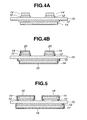
- the sample was dipped in amixed solution containing 1.4 % EDTA, 6 % hydrogenperoxide and 3 % ammonia to remove undesired portions of the brazing filler metal 12 (FIG. 3A).
- the design value of a chip mounting portion was 11 mm x 11 mm (the bottom face of the copper plate) .
- ultraviolet curing alkali peeling resists 18 having a desired circuit pattern were applied on both faces of the copper plates 14 again (FIG.
- the weight of metal powder containing metal components was measured so that the components are 91 Ag - 7 Cu -1.5 Ti - 0.5 TiO 2 (wt%).
- To this metal powder about 10 % of an acrylic vehicle was added.
- a paste-like brazing filler metal was prepared.
- a ceramic substrate 10 was prepared (FIG. 1A), and the brazing filler metal 12 was applied on both faces of the ceramic substrate 10 by the screen printing (FIG. 1B). Then, copper plates 14 having a thickness of 0.25 mm were arranged on both side thereof, and the copper plates 14 were bonded to the ceramic substrate 10 at 835 °C in a vacuum furnace. In order to verify the thickness of the brazing filler metal 12, the sample thus bonded was cut to measure the thickness of the brazing filler metal 12. As a result, the thickness of the brazing filler metal 12 was about 20 ⁇ m.
- the ceramic substrate 10 an S grade AlN substrate produced by ATG company was used.
- FIGS. 2A through 2C ultraviolet curing alkali peeling resists 16 having a desired circuit pattern and a thickness of 10 to 15 ⁇ m were applied on both faces of the bonded copper plates 14 (FIG. 2A), and undesired portions of the copper plates 14 were removed with an etchant comprising copper chloride, aqueous hydrogen peroxide and hydrochloric acid (FIG. 2B). Thereafter, the resists 16 were removed with an aqueous solution of 3.5 % sodium hydroxide (FIG. 2C).
- etching In the etching at this time, larger masks than usual masks by 50 ⁇ m were used as the resists 16 in view of correction carried out by etching, and conditions, such as the conveyer speed of the etching machine and the spray pressure of the etchant, were controlled so as to provide a difference of 20 ⁇ m or less between the top and bottom portions of the copper plate and so as to meet the dimensional precision.
- the design value of a chip mounting portion was 11 mm x 11 mm (the bottom face of the copper plate) .
- the sample was dipped in amixed solution containing 1.4 % EDTA, 6 % hydrogen peroxide and 3 % ammonia to remove undesired portions of the brazing filler metal 12 (FIG. 3A) . Thereafter, an Ni-P electroless plating 20 was carried out on the surfaces of the copper plates 14 and brazing filler metal 12 (FIG. 5).
- Samples were prepared by the same method as that in Example 2, except that the thickness of the copper plate was 0.2 mm and the dimension of the chip mounting portion was 0.8 mm x 1.8 mm.
- Samples were prepared by the same method as that in Example 2, except that the skirt spreading length was 100 ⁇ m. Furthermore, the ratio of the area of the top face of the metal plate of the sample prepared in each of Examples 1 and 2 to the area of the top face of the metal plate of the sample prepared in this comparative example is 103 %.
- Samples were prepared by the same method as that in Example 3, except that the skirt spreading lengthwas 100 ⁇ m. Furthermore, the ratio of the area of the top face of the metal plate of the sample prepared in Example 3 to the area of the top face of the metal plate of the sample prepared in this comparative example is 139 %.
- the skirt spreading length of a metal plate is less than 50 ⁇ m, so that it is possible to realize a reliable chip mounting.
- the margin in design can be set even in the case of a smaller substrate.
- the ratio of the area of the top face of the metal plate before the change of the skirt spreading length to that after the change of the skirt spreading length is a large value, and the margin in design around a chip is very large when the chip is mounted, so that it is possible to greatly improve the reliability of the chip mounting and prevent the displacement of the chip.
Landscapes
- Engineering & Computer Science (AREA)
- Chemical & Material Sciences (AREA)
- Ceramic Engineering (AREA)
- Manufacturing & Machinery (AREA)
- Microelectronics & Electronic Packaging (AREA)
- Materials Engineering (AREA)
- Structural Engineering (AREA)
- Organic Chemistry (AREA)
- Manufacturing Of Printed Wiring (AREA)
- Structure Of Printed Boards (AREA)
- Insulated Metal Substrates For Printed Circuits (AREA)
- Ceramic Products (AREA)
Claims (9)
- Metall-/Keramik-Leiterplatte umfassend:ein Keramiksubstrat (10) undeine auf dem Keramiksubstrat (10) angeordnete Metallleiterplatte (14), wobei die Metallleiterplatte (14) eine Dicke zwischen 0,1 mm und 0,5 mm aufweist und die Metallleiterplatte (14) eine Randausdehnung (L1) von weniger als 50 µm aufweist, wobei die Randausdehnung (L1) die Entfernung zwischen einer zu einer Hauptebene der Metallplatte (14) an einem Ende der Bodenfläche der Metallplatte (14) senkrechten Ebene und einer zu einer Hauptebene der Metallplatte (14) an einem Ende der Deckfläche der Metallplatte (14) auf derselben Seite wie das eine Ende der Bodenfläche der Metallplatte (14) senkrechten Ebene ist, angenommen, dass die Entfernung positiv ist, wenn die Bodenfläche eine größere Fläche aufweist als die der Deckfläche, dadurch gekennzeichnet, dass auf der Metall-/Keramik-Leiterplatte ein Superleistungsteil montiert ist oder dass die Metall-/Keramik-Leiterplatte ein feines Muster aufweist, auf dem ein Peltier-Element oder eine Hochfrequenzschaltung montiert ist.
- Metall-/Keramik-Leiterplatte nach Anspruch 1, wobei die Metallleiterplatte (14) direkt mit dem Keramiksubstrat (10) verbunden ist.
- Metall-/Keramik-Leiterplatte nach Anspruch 1, wobei die Metallleiterplatte (14) durch Nickelplattieren, Nickellegierungsplattieren, Goldplattieren oder Konservieren behandelt ist.
- Metall-/Keramik-Leiterplatte nach Anspruch 1, wobei die Metallleiterplatte (14) mit dem Keramiksubstrat (10) über ein Lötzusatzmetall (12) verbunden ist.
- Metall-/Keramik-Leiterplatte nach Anspruch 4, wobei das Lötzusatzmetall (12) aus einem Material ausgewählt aus der Gruppe bestehend aus Legierungen und Verbindungen enthaltend Silber und ein aktives Metall, Legierungen und Verbindungen enthaltend Aluminium sowie Mischungen hiervon gefertigt ist.
- Metall-/Keramik-Leiterplatte nach Anspruch 4, wobei die Metallleiterplatte (14) und das Lötzusatzmetall (12) durch Nickelplattieren, Nickellegierungsplattieren, Goldplattieren oder Konservieren behandelt sind.
- Metall-/Keramik-Leiterplatte nach Anspruch 1, wobei das Keramiksubstrat (10) aus einem Material ausgewählt aus der Gruppe bestehend aus Oxiden, Nitriden und Carbiden gebildet ist.
- Metall-/Keramik-Leiterplatte nach Anspruch 1, wobei die Metallleiterplatte (14) aus einem Material ausgewählt aus der Gruppe bestehend aus Kupfer, Aluminium und Legierungen hiervon gebildet ist.
- Modul aufgebaut durch Verwendung einer Metall-/Keramik-Leiterplatte nach Anspruch 1.
Applications Claiming Priority (2)
| Application Number | Priority Date | Filing Date | Title |
|---|---|---|---|
| JP2001304513A JP3648189B2 (ja) | 2001-09-28 | 2001-09-28 | 金属−セラミックス回路基板 |
| JP2001304513 | 2001-09-28 |
Publications (3)
| Publication Number | Publication Date |
|---|---|
| EP1298968A2 EP1298968A2 (de) | 2003-04-02 |
| EP1298968A3 EP1298968A3 (de) | 2005-02-02 |
| EP1298968B1 true EP1298968B1 (de) | 2006-06-07 |
Family
ID=19124423
Family Applications (1)
| Application Number | Title | Priority Date | Filing Date |
|---|---|---|---|
| EP02021755A Expired - Lifetime EP1298968B1 (de) | 2001-09-28 | 2002-09-25 | Metall bekleidete keramische Schaltungsplatte |
Country Status (4)
| Country | Link |
|---|---|
| US (1) | US6686030B2 (de) |
| EP (1) | EP1298968B1 (de) |
| JP (1) | JP3648189B2 (de) |
| DE (1) | DE60212027T2 (de) |
Families Citing this family (22)
| Publication number | Priority date | Publication date | Assignee | Title |
|---|---|---|---|---|
| US6936337B2 (en) * | 2001-09-28 | 2005-08-30 | Dowa Mining Co., Ltd. | Metal/ceramic circuit board |
| JP3863067B2 (ja) * | 2002-06-04 | 2006-12-27 | Dowaホールディングス株式会社 | 金属−セラミックス接合体の製造方法 |
| JP3868854B2 (ja) * | 2002-06-14 | 2007-01-17 | Dowaホールディングス株式会社 | 金属−セラミックス接合体およびその製造方法 |
| JP4362597B2 (ja) * | 2003-05-30 | 2009-11-11 | Dowaメタルテック株式会社 | 金属−セラミックス回路基板およびその製造方法 |
| CN100508698C (zh) * | 2003-09-25 | 2009-07-01 | 株式会社东芝 | 陶瓷电路板、其生产方法以及电源模块 |
| DE102004030800B4 (de) | 2004-06-25 | 2017-05-18 | Epcos Ag | Verfahren zur Herstellung einer keramischen Leiterplatte |
| EP1791176B1 (de) * | 2004-08-17 | 2019-07-03 | Mitsubishi Materials Corporation | Herstellungsverfahren eines leistungsmodulsubstrats |
| JP5413707B2 (ja) * | 2005-06-06 | 2014-02-12 | Dowaエレクトロニクス株式会社 | 金属−セラミック複合基板及びその製造方法 |
| TW201037803A (en) * | 2009-04-13 | 2010-10-16 | High Conduction Scient Co Ltd | Multi-layer packaging substrate, method for making the packaging substrate, and package structure of light-emitting semiconductor |
| EP3273755B1 (de) * | 2009-09-15 | 2018-11-07 | Kabushiki Kaisha Toshiba | Verfahren zur herstellung einer keramikleiterplatte |
| JP5516696B2 (ja) * | 2012-11-01 | 2014-06-11 | 株式会社豊田自動織機 | 基板 |
| CN103862898A (zh) * | 2014-02-28 | 2014-06-18 | 奥士康精密电路(惠州)有限公司 | 一种线路板蓝胶印刷工艺 |
| DE102014220650A1 (de) * | 2014-10-13 | 2016-04-14 | Heraeus Deutschland GmbH & Co. KG | Optimiertes Leiterbahndesign von metallischen Materialien auf keramischen Substanzen |
| EP3321957B1 (de) * | 2015-07-09 | 2022-07-27 | Kabushiki Kaisha Toshiba | Keramik-metall-leiterplatte und halbleiterbauelement damit |
| EP3358614B1 (de) * | 2015-09-28 | 2022-12-14 | Kabushiki Kaisha Toshiba | Schaltsubstrat und halbleiterbauelement |
| JP7230432B2 (ja) * | 2017-11-02 | 2023-03-01 | 三菱マテリアル株式会社 | 接合体、及び、絶縁回路基板 |
| CN108346952B (zh) * | 2018-01-25 | 2020-11-24 | 番禺得意精密电子工业有限公司 | 电连接器固持装置 |
| JP7332588B2 (ja) * | 2018-05-16 | 2023-08-23 | 株式会社東芝 | セラミックス銅回路基板およびその製造方法 |
| JP7739105B2 (ja) * | 2021-09-21 | 2025-09-16 | Dowaメタルテック株式会社 | 金属-セラミックス接合基板およびその製造方法 |
| EP4482262A4 (de) * | 2022-03-16 | 2025-06-04 | Denka Company Limited | Keramisches verbundsubstrat und verfahren zur herstellung eines keramischen verbundsubstrats |
| WO2023176376A1 (ja) * | 2022-03-16 | 2023-09-21 | デンカ株式会社 | セラミック複合基板、及びセラミック複合基板の製造方法 |
| WO2025134898A1 (ja) * | 2023-12-22 | 2025-06-26 | 株式会社 東芝 | セラミックス回路基板及びその製造方法 |
Family Cites Families (8)
| Publication number | Priority date | Publication date | Assignee | Title |
|---|---|---|---|---|
| US5014159A (en) * | 1982-04-19 | 1991-05-07 | Olin Corporation | Semiconductor package |
| DE4406397A1 (de) * | 1994-02-26 | 1995-08-31 | Curamik Electronics Gmbh | Substrat für elektrische Schaltkreise sowie Verfahren zum Herstellen des Substrates |
| JP3512977B2 (ja) * | 1996-08-27 | 2004-03-31 | 同和鉱業株式会社 | 高信頼性半導体用基板 |
| EP0935286A4 (de) * | 1997-05-26 | 2008-04-09 | Sumitomo Electric Industries | Kupfer-schaltungsverbindungssubstrat und seine herstellung |
| JP3449458B2 (ja) * | 1997-05-26 | 2003-09-22 | 電気化学工業株式会社 | 回路基板 |
| JPH11322455A (ja) * | 1998-05-14 | 1999-11-24 | Tokuyama Corp | セラミックス/金属接合体およびその製造方法 |
| JP4334054B2 (ja) * | 1999-03-26 | 2009-09-16 | 株式会社東芝 | セラミックス回路基板 |
| JP2001210948A (ja) * | 2000-01-21 | 2001-08-03 | Kyocera Corp | セラミック回路基板 |
-
2001
- 2001-09-28 JP JP2001304513A patent/JP3648189B2/ja not_active Expired - Lifetime
-
2002
- 2002-09-25 EP EP02021755A patent/EP1298968B1/de not_active Expired - Lifetime
- 2002-09-25 DE DE60212027T patent/DE60212027T2/de not_active Expired - Lifetime
- 2002-09-25 US US10/254,724 patent/US6686030B2/en not_active Expired - Lifetime
Also Published As
| Publication number | Publication date |
|---|---|
| JP3648189B2 (ja) | 2005-05-18 |
| EP1298968A3 (de) | 2005-02-02 |
| EP1298968A2 (de) | 2003-04-02 |
| JP2003110205A (ja) | 2003-04-11 |
| DE60212027D1 (de) | 2006-07-20 |
| US20030068537A1 (en) | 2003-04-10 |
| US6686030B2 (en) | 2004-02-03 |
| DE60212027T2 (de) | 2006-12-28 |
Similar Documents
| Publication | Publication Date | Title |
|---|---|---|
| EP1298968B1 (de) | Metall bekleidete keramische Schaltungsplatte | |
| EP1298108B1 (de) | Metall-keramik Verbundgegenstand | |
| EP1298970B1 (de) | Verfahren zur Herstellung einer Metall/Keramik-Verbundleiterplatte | |
| EP2259308B1 (de) | Substrat für leistungsmodul mit kühlkörper und herstellungsverfahren dafür, leistungsmodul mit kühlkörper und substrat für leistungsmodul | |
| EP0339881B1 (de) | Verfahren zum Herstellen einer Leiterplatte | |
| EP0874399A1 (de) | Siliziumnitrid-leiterplatte und halbleiter-modul | |
| EP1482771B1 (de) | Metall/Keramik-Leiterplatte und deren Verfahren zur Herstellung | |
| EP1039539B1 (de) | Herstellungsmethode für eine Keramikleiterplatte | |
| US6936337B2 (en) | Metal/ceramic circuit board | |
| JP3449458B2 (ja) | 回路基板 | |
| JP5002614B2 (ja) | セラミックス回路基板の製造方法 | |
| JP2001185664A (ja) | セラミックス回路基板 | |
| JP2004307307A (ja) | セラミックス回路基板とその製造方法 | |
| JP3531133B2 (ja) | パワーモジュール用基板及びその製造法 | |
| JPH10242330A (ja) | パワーモジュール用基板及びその製造法 | |
| KR20040043530A (ko) | 금속/세라믹 접합 제품 | |
| JP3729637B2 (ja) | 電子部品 | |
| JP2000049427A (ja) | 接合体及びそれを用いた回路基板 | |
| JP7208439B2 (ja) | セラミックス回路基板、電子デバイス、金属部材、及びセラミックス回路基板の製造方法 | |
| JP3155885B2 (ja) | 回路基板 | |
| JP2000086367A (ja) | 接合体及びそれを用いた回路基板 | |
| EP4033524A1 (de) | Leiterplatte und modul damit | |
| WO2024195329A1 (ja) | 銅-セラミックス回路基板およびその製造方法 | |
| JP3354002B2 (ja) | 回路基板の製造方法 | |
| JPH06105822B2 (ja) | セラミックス回路基板 |
Legal Events
| Date | Code | Title | Description |
|---|---|---|---|
| PUAI | Public reference made under article 153(3) epc to a published international application that has entered the european phase |
Free format text: ORIGINAL CODE: 0009012 |
|
| AK | Designated contracting states |
Kind code of ref document: A2 Designated state(s): AT BE BG CH CY CZ DE DK EE ES FI FR GB GR IE IT LI LU MC NL PT SE SK TR |
|
| AX | Request for extension of the european patent |
Extension state: AL LT LV MK RO SI |
|
| PUAL | Search report despatched |
Free format text: ORIGINAL CODE: 0009013 |
|
| AK | Designated contracting states |
Kind code of ref document: A3 Designated state(s): AT BE BG CH CY CZ DE DK EE ES FI FR GB GR IE IT LI LU MC NL PT SE SK TR |
|
| AX | Request for extension of the european patent |
Extension state: AL LT LV MK RO SI |
|
| RIC1 | Information provided on ipc code assigned before grant |
Ipc: 7H 01L 23/373 B Ipc: 7H 05K 1/02 B Ipc: 7H 05K 3/06 B Ipc: 7H 05K 1/03 A |
|
| 17P | Request for examination filed |
Effective date: 20050421 |
|
| 17Q | First examination report despatched |
Effective date: 20050520 |
|
| AKX | Designation fees paid |
Designated state(s): DE FR GB NL |
|
| GRAP | Despatch of communication of intention to grant a patent |
Free format text: ORIGINAL CODE: EPIDOSNIGR1 |
|
| GRAS | Grant fee paid |
Free format text: ORIGINAL CODE: EPIDOSNIGR3 |
|
| GRAA | (expected) grant |
Free format text: ORIGINAL CODE: 0009210 |
|
| AK | Designated contracting states |
Kind code of ref document: B1 Designated state(s): DE FR GB NL |
|
| REG | Reference to a national code |
Ref country code: GB Ref legal event code: FG4D |
|
| REF | Corresponds to: |
Ref document number: 60212027 Country of ref document: DE Date of ref document: 20060720 Kind code of ref document: P |
|
| ET | Fr: translation filed | ||
| PLBE | No opposition filed within time limit |
Free format text: ORIGINAL CODE: 0009261 |
|
| STAA | Information on the status of an ep patent application or granted ep patent |
Free format text: STATUS: NO OPPOSITION FILED WITHIN TIME LIMIT |
|
| 26N | No opposition filed |
Effective date: 20070308 |
|
| REG | Reference to a national code |
Ref country code: FR Ref legal event code: PLFP Year of fee payment: 15 |
|
| REG | Reference to a national code |
Ref country code: FR Ref legal event code: PLFP Year of fee payment: 16 |
|
| REG | Reference to a national code |
Ref country code: FR Ref legal event code: PLFP Year of fee payment: 17 |
|
| PGFP | Annual fee paid to national office [announced via postgrant information from national office to epo] |
Ref country code: NL Payment date: 20210813 Year of fee payment: 20 |
|
| PGFP | Annual fee paid to national office [announced via postgrant information from national office to epo] |
Ref country code: FR Payment date: 20210812 Year of fee payment: 20 |
|
| PGFP | Annual fee paid to national office [announced via postgrant information from national office to epo] |
Ref country code: DE Payment date: 20210818 Year of fee payment: 20 Ref country code: GB Payment date: 20210818 Year of fee payment: 20 |
|
| REG | Reference to a national code |
Ref country code: DE Ref legal event code: R071 Ref document number: 60212027 Country of ref document: DE |
|
| REG | Reference to a national code |
Ref country code: NL Ref legal event code: MK Effective date: 20220924 |
|
| REG | Reference to a national code |
Ref country code: GB Ref legal event code: PE20 Expiry date: 20220924 |
|
| PG25 | Lapsed in a contracting state [announced via postgrant information from national office to epo] |
Ref country code: GB Free format text: LAPSE BECAUSE OF EXPIRATION OF PROTECTION Effective date: 20220924 |