EP1300944A2 - Dispositif à gain variable et dispositif de communication sans fil - Google Patents
Dispositif à gain variable et dispositif de communication sans fil Download PDFInfo
- Publication number
- EP1300944A2 EP1300944A2 EP02022304A EP02022304A EP1300944A2 EP 1300944 A2 EP1300944 A2 EP 1300944A2 EP 02022304 A EP02022304 A EP 02022304A EP 02022304 A EP02022304 A EP 02022304A EP 1300944 A2 EP1300944 A2 EP 1300944A2
- Authority
- EP
- European Patent Office
- Prior art keywords
- variable gain
- switching element
- amplifying apparatus
- gain amplifying
- amplifier
- Prior art date
- Legal status (The legal status is an assumption and is not a legal conclusion. Google has not performed a legal analysis and makes no representation as to the accuracy of the status listed.)
- Withdrawn
Links
Images










Classifications
-
- H—ELECTRICITY
- H03—ELECTRONIC CIRCUITRY
- H03G—CONTROL OF AMPLIFICATION
- H03G1/00—Details of arrangements for controlling amplification
- H03G1/0005—Circuits characterised by the type of controlling devices operated by a controlling current or voltage signal
- H03G1/0088—Circuits characterised by the type of controlling devices operated by a controlling current or voltage signal using discontinuously variable devices, e.g. switch-operated
Definitions
- the present invention relates to a variable gain amplifying apparatus having a gain control function, and a wireless communication apparatus.
- a pre-stage amplifier of a reception device in a radio system represented by cellular phones needs to have low-noise and high-gain characteristics if receiving very weak signals, and the pre-amplifier needs to have low-distortion and low-gain characteristics if receiving large signals.
- the reception device since the electric field intensity during reception varies significantly depending on the distance between a base station and a mobile station, the reception device requires a large dynamic range, and consequently the pre-amplifier of the reception device needs to have a gain control function.
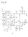
- FIG. 21 shows the circuit configuration of main parts of a cellular phone terminal in which a conventional variable gain amplifying apparatus having this gain control function is used.
- the cellular phone terminal of FIG. 21 is used in digital radio communications using modulation systems such as QPSK.
- the cellular phone terminal is comprised of an antenna 1, a duplexer 2, a transmission circuit portion 3, a variable gain amplifying apparatus 4, a mixer 7, a filter 8, mixers 9, 10, a local oscillator 11 and a phase shifter 12.
- the variable gain amplifying apparatus 4, the mixer 7, the filter 8, the mixers 9, 10, the local oscillator 11 and the phase shifter 12 constitute a reception circuit portion.
- the mixer 9, the mixer 10, the local oscillator 11 and the phase shifter 12 constitute an orthogonal demodulator.
- the antenna 1 sends a send signal as a send wave, and receives a receive wave as a receive signal.
- the duplexer 2 guides the send signal outputted from the transmission circuit 3 to the antenna 1, and guides the receive wave received at the antenna 1 to the variable gain amplifying apparatus 4.
- the variable gain amplifying apparatus 4 is a circuit that amplifies the receive signal as the pre-amplifier of the reception circuit portion.
- the mixer 7 is a circuit that combines the signal inputted form an oscillator (not shown) with the receive signal amplified by the variable gain amplifying apparatus 4, thereby converting the amplified signal into an intermediate frequency signal.
- the filter 8 is a circuit that weakens unnecessary frequency components of the signal converted into the intermediate frequency signal.
- the mixer 10 is a circuit that combines together the signal outputted from the filter 8 and the signal inputted from the local oscillator 11, thereby demodulating a base band I signal.
- the mixer 9 is a circuit that combines together the signal outputted from the filter 8 and the signal with its phase shifted by an angle of 90 degrees by the phase shifter 12, thereby demodulating a base band Q signal.
- the phase shifter 12 is a circuit that shifts the phase of the signal oscillated by the local oscillator 11 by an angle of 90 degrees.
- variable gain amplifying apparatus 4 is comprised of an amplifier 5 and a switching element 6.
- the receive signal received at the antenna 1 is amplified by the variable gain amplifying apparatus 4 via the duplexer 2.
- the mixer 7 converts the receive signal amplified by the variable gain amplifying apparatus 4 into the intermediate frequency signal, and the filter 8 weakens unnecessary frequency components of the converted intermediate frequency signal.
- the signal from the local oscillator 11 is outputted to the mixer 10 and the phase shifter 12.
- the mixer 10 combines together the output signal from the filter 8 and the signal inputted from the local oscillator 11, thereby demodulating the base band I signal.
- the phase shifter 12 outputs to the mixer 9 the signal with its phase shifted by an angle of 90 degrees coming from the local oscillator 11, and the mixer 9 combines together the output signal from the filter 8 and the signal from the phase shifter 12, thereby demodulating the base band Q signal.
- the demodulated base band I signal and base band Q signal are inputted to a base band portion (not shown) , where they are restored to digital voice data.
- variable gain amplifying apparatus 4 If the cellular phone terminal exists within close range of the base station, and so on, the magnitude of the receive signal received at the antenna 1 is large. In this case, a large receive signal is inputted to the variable gain amplifying apparatus 4 as well. In this case, the supply to the variable gain amplifying apparatus 4 of a power voltage for operating the amplifier 5 is stopped, and the switching element 6 is controlled so that it becomes enabled. Therefore, the large receive signal inputted from the duplexer 2 is outputted to the mixer 7 through the switching element 6 without being amplified by the amplifier 5. That is, the variable gain amplifying apparatus 4 operates in a low gain mode. In this way, the variable gain amplifying apparatus 4 operates in a low gain mode when the magnitude of the receive signal is large.
- variable gain amplifying apparatus 4 is supplied with a power voltage for operating the amplifier 5, and the switching element 6 is controlled so that it becomes disabled. Therefore, the very weak receive signal inputted from the duplexer 2 is amplified by the amplifier 5 and then outputted to the mixer 7 without passing through the switching element 6. That is, the variable gain amplifying apparatus 4 operates in a high gain mode. In this way, the variable gain amplifying apparatus 4 operates in a high gain mode when the intensity of the receive signal is very low.
- variable gain amplifying apparatus 4 operates in a low gain mode when the magnitude of the receive signal is large, and operates in a high gain mode when the intensity of the receive signal is very low, and therefore the variable gain amplifying apparatus 4 can have a wide dynamic range.
- the inventor has found that the amount of phase shift of the receive signal passed through the variable gain amplifying apparatus 4 when the variable gain amplifying apparatus 4 operates in a low gain mode is different from the amount of phase shift of the receive signal passed through the variable gain amplifying apparatus 4 when the variable gain amplifying apparatus 4 operates in a high gain mode.
- variable gain amplifying apparatus 4 when the variable gain amplifying apparatus 4 is switched from the low gain mode to the high gain mode, or switched from the high gain mode to the low gain mode, the phase of the signal outputted from the variable gain amplifying apparatus 4 is shifted in a discontinuous manner, thus making it impossible to provide synchronization in the orthogonal demodulator constituted by the mixer 9, the mixer 10, the local oscillator 11 and the phase shifter 12. Therefore, the base band I signal and the base band Q signal cannot be demodulated normally in the orthogonal demodulator until synchronization can be provided.
- the output signal cos ⁇ t from the local oscillator 11 is inputted to a phase shifter 12, and the phase shifter 12 shifts the phase by an angle of 90 degrees, thereby outputting the signal of sin ⁇ t to the mixer 9.
- the signal outputted from the phase shifter 12 and the input signal to the orthogonal demodulator are combined together, and thus the output signal from the mixer 9 is expressed by the following equation 4.
- the base band I signal and the base band Q signal can be demodulated normally by the orthogonal demodulator.
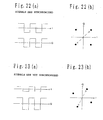
- FIG. 22(A) Examples of values of the demodulated base band I signal and base band Q signal expressed by the equations 3 and 5, respectively, are shown in FIG. 22(A). That is, in FIG. 22(B), the values of I(t) and Q(t) are identical to each other, and change with time from +1 to -1 to +1...
- FIG. 22(B) shows a plot with the base band I signal on the horizontal axis and the base band Q signal on the vertical axis for given values of I(t) and Q(t).
- the pair of the base band I signal and base band Q signal shown in FIG. 22(A) is plotted in the first and third quadrant in FIG. 22(B). When a straight line is drawn along the plotted spots, the line slants at an angle of 45° relative to the horizontal axis.
- variable gain amplifying apparatus 4 is switched from the low gain mode to the high gain mode, or switched from the high gain mode to the low gain mode.
- the amount of phase shift of the receive signal passed through the variable gain amplifying apparatus 4 when the variable gain amplifying apparatus 4 operates in the low gain mode is different from the amount of phase shift of the receive signal passed through the variable gain amplifying apparatus 4 when the variable gain amplifying apparatus 4 operates in the high gain mode. Therefore, the phase of the input signal S(t) to the orthogonal demodulator is shifted by ⁇ .
- the output signal cos ⁇ t from the local oscillator 11 is inputted to a phase shifter 12, and the phase shifter 12 shifts the phase by an angle of 90 degrees, thereby outputting the signal of sin ⁇ t to the mixer 9.
- the signal outputted from the phase shifter 12 and the input signal to the orthogonal demodulator are combined together, and thus the output signal from the mixer 9 is expressed by the following equation 9.
- S(t) ⁇ sin ⁇ t I(t) ⁇ (1/2) ⁇ (sin ⁇ + sin2 ⁇ t) + Q(t) ⁇ (1/2) ⁇ (cos ⁇ -cos2 ⁇ t)
- the demodulated base band I signal and base bandQ signal are changed to those shown in FIG. 23.
- the situation shown in FIG. 22(A) is changed to that shown in FIG. 23(A)
- the associated plot shown in FIG. 22(B) is changed to that shown in FIG. 23(B).
- the pair of the base band I signal and base band Q signal shown in FIG. 23(A) is plotted in the first and third quadrants in FIG. 23(B), but when a straight line is drawn along the plotted spots, the line slants at an angle larger than 45° relative to the horizontal axis.
- the pair of values of the demodulated base band I signal and base band Q signal is expressed by (1, 1) in FIG. 22(A)
- the pair of values may be shifted to the second quadrant when the mode of the variable gain amplifying apparatus 4 is switched. In some cases, the pair of values may be shifted to the third quadrant.
- the base band I signal and base band Q signal can be demodulated normally until the local oscillator 11 is synchronized with the input signal to the orthogonal demodulator after the mode of the variable gain amplifying apparatus 4 is switched, and therefore the voice digital signal can be restored normally, which may cause disconnection of received voices of the cellular phone terminal and occurrence of noises.
- the object of the present invention is to provide a variable gain amplifying apparatus capable of sufficiently alleviating the situation in which the phase outputted from the variable gain amplifying apparatus is shifted in a discontinuous manner even when the gain of the variable gain amplifying apparatus is switched, and a wireless communication apparatus.
- the 1st invention of the present invention is a variable gain amplifying apparatus comprising:
- the 2nd invention of the present invention is a variable gain amplifying apparatus comprising:
- the 3rd invention of the present invention is the variable gain amplifying apparatus according to the 1st invention, wherein said first switching element is comprised of one or more third switching elements and one or more fourth switching elements, one end of said third switching element is connected to the input of said amplifier, the other end of said third switching element is connected to one end of said phase shifter, the other end of said phase shifter is connected to one end of said fourth switching element, and the other end of said fourth switching element is connected to the output of said amplifier.
- the 4th invention of the present invention is the variable gain amplifying apparatus according to the 2nd invention, wherein said first switching element is comprised of one or more third switching elements and one or more fourth switching elements, one end of said third switching element is connected to the input of said amplifier, the other end of said third switching element is connected to one end of said phase shifter, the other end of said phase shifter is connected to one end of said fourth switching element, and the other end of said fourth switching element is connected to the output of said amplifier.
- the 5th invention of the present invention is a variable gain amplifying apparatus comprising:
- the 6th invention of the present invention is the variable gain amplifying apparatus according to any of the 1st to 5th inventions, wherein said phase shifter is comprised of one or more serial-connected capacitors and one or more parallel-connected resistors.
- the 7th invention of the present invention is the variable gain amplifying apparatus according to any of the 1st to 5th inventions, wherein said phase shifter is comprised of one or more serial-connected resistors and one or more parallel-connected capacitors.
- the 8th invention of the present invention is the variable gain amplifying apparatus according to any of the 1st to 5th inventions, wherein said phase shifter is comprised of one or more strip lines, and said strip lines are connected so that a characteristic impedance monotonously increases or monotonously decreases.
- the 9th invention of the present invention is the variable gain amplifying apparatus according to any of the 1st to 5th inventions, wherein said phase shifter is comprised of one or more parallel twin lines, and said parallel twin lines are connected so that a characteristic impedance monotonously increases or monotonously decreases.
- the 10th invention of the present invention is the variable gain amplifying apparatus according to any of the 1st to 5th inventions , wherein said phase shifter is comprised of one or more serial-connected capacitors and one or more parallel-connected inductors.
- the 11th invention of the present invention is the variable gain amplifying apparatus according to any of the 1st to 5th inventions, wherein said phase shifter is comprised of one or more serial-connected inductors and one or more parallel-connected capacitors.
- the 12th invention of the present invention is the variable gain amplifying apparatus according to any of the 1st to 5th inventions, wherein one end or both ends of said switching element are connected to the ground through the resistor or the inductor.
- the 13th invention of the present invention is a wireless communication apparatus comprising the variable gain amplifying apparatus according to any of the 1st to 5th inventions, and using phase modulation signals as send/receive signals.
- the 14th invention of the present invention is a wireless communication apparatus comprising:
- the 15th invention of the present invention is a wireless communication apparatus comprising:
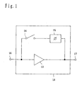
- variable gain amplifying apparatus 18 of this embodiment is shown in FIG. 1.
- the variable gain amplifying apparatus 18 is used as, for example, a variable gain amplifying apparatus 4 of a cellular phone terminal of FIG. 21.
- variable gain amplifying apparatus 18 is comprised of an amplifier 13, a switching element 14 and a phase shifter 15.
- the amplifier 13 has its input connected to an input terminal 16 and its output connected to an output terminal 17.
- the switching element 14 is connected at one end to the input of the amplifier 13 and connected at the other end to one end of the phase shifter 15.
- the other end of the phase shifter 15 is connected to the output of the amplifier 13.
- the input terminal 16 is a terminal to which the receive signal outputted from the front stage of a duplexer 2 of FIG. 21 is inputted
- the output terminal 17 is a terminal for outputting the signal amplified in the variable gain amplifying apparatus 18 to the rear stage of a mixer 7 of FIG. 21 and the like.
- variable gain amplifying apparatus 18 of this embodiment has a configuration such that the switching element 14 is connected in parallel to the amplifier 13, and the phase shifter 15 is connected in series to the switching element 14.
- variable gain amplifying apparatus 18 of this embodiment is operated by being controlled in accordance with a control circuit (not shown) .
- the control circuit controls the operation of the variable gain amplifying apparatus 18 depending on the level of the receive signal received at the antenna 1.
- control is performed so that the switching element 14 is enabled if the level of the input signal is higher than a predetermined level, and the switching element 14 is disabled if the level of the input signal is equal to or lower than the predetermined level.
- control is performed so that the amplifier 13 does not operate when the switching element 14 is enabled, and the amplifier 13 operates when the switching element 14 is disabled.
- This control is performed by, for example, supplying a power voltage for operating the amplifier 13 when the amplifier 13 is to be operated, and stopping the supply of a power voltage for operating the amplifier 13 when the operation of the amplifier 13 is to be stopped.
- variable gain amplifying apparatus 13 operates in the low gain mode if the level of the receive signal is higher than a predetermined level. That is, since the switching element is enabled and the amplifier 13 stops its operation, the receive signal is inputted from the input terminal 16, passed through the switching element 14 and the phase shifter 15, and outputted from the output terminal 17.
- variable gain amplifying apparatus 18 operates in the high gain mode if the level of the receive signal is equal to or lower than the predetermined level. That is, since the switching element is disabled and the amplifier 13 operates, the receive signal is inputted from the input terminal 16, amplified by the amplifier 13, and outputted from the output terminal 17.
- the phase shifter 15 shifts the phase of the receive signal inputted to the phase shifter 15 so that the amount of phase shift of the receive signal when the receive signal is passed through the amplifier is substantially equal to the amount of phase shift of the receive signal when the receive signal is passed through the switching element 14 and the phase shifter 15.
- variable gain amplifying apparatus 18 is switched from the high gain mode to the low gain mode, or switched from the low gain mode to the high gain mode, the phase of the signal outputted from the output terminal 17 is not shifted in a discontinuous manner.
- variable gain amplifying apparatus 18 of this embodiment in the pre-amplifier of the reception apparatus in the radio system represented by cellular phones , cellular phone terminals and the like with high quality of received voice can be provided.
- the switching element 14 is connected to the input of the amplifier 13, and the phase shifter 15 is connected to the output of the amplifier 13, but the invention is not limited to this configuration.
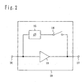
- variable gain amplifying apparatus 19 having a configuration different from that of FIG. 1 is shown in FIG. 2.
- the switching element 14 is connected to the output of the amplifier 13, and the phase shifter 15 is connected to the input of the amplifier 13.
- the positions of the switching element 14 and the phase shifter 15 in the variable gain amplifying apparatus 18 are changed to each other. That is, one end of the phase shifter 15 is connected to the input of the amplifier 13, the other end of the phase shifter 15 is connected to one end of the switching element 14, and the other end of the switching element 14 is connected to the output of the amplifier 13.
- Use of the variable gain amplifying apparatus 19 makes it possible to attain a same degree of effectiveness as that described above.
- variable gain amplifying apparatus 21 having a configuration different from that of FIG. 1 is shown in FIG. 3. Unlike the variable gain amplifying apparatus 18 of FIG. 1, the variable gain amplifying apparatus 21 comprises two switching elements. Specifically, in the variable gain amplifying apparatus 21, one end of the switching element 14 is connected to the input of the amplifier 13, the other end of the switching element 14 is connected to the phase shifter 15, the other end of the phase shifter 15 is connected to one end of a switching element 20, and the other end of the switching element 20 is connected to the output of the amplifier 13.
- the switching elements 14, 20 are enabled if the level of the receive signal inputted from the input terminal 16 is higher than a predetermined level, and the switching elements 14, 20 are disabled if the lever of the receive signal inputted from the input terminal 16 is equal to or lower than the predetermined level.
- the power voltage for operating the amplifier 13 is controlled as in the case of the above embodiment, so that the amplifier 13 does not operate when the switching elements 14 and 20 are enabled, and the amplifier 13 operates when the switching elements 14 and 20 are disabled.
- the phase shifter 15 shifts the phase of the receive signal inputted to the phase shifter 15 so that the amount of phase shift of the receive signal when the receive signal inputted from the input terminal 16 is passed through the amplifier 13 is substantially equal to the amount of phase shift of the receive signal when the receive signal inputted from the input terminal 16 is passed through the switching element 14, the phase shifter 15 and the switching element 20.
- variable gain amplifying apparatus 18 of FIG. 1 if the level of the receive signal inputted to the input terminal 16 is equal to or lower than a predetermined level, the switching element 14 is disabled, but the other end of the phase shifter 15 is still connected to the output of the amplifier 13. Therefore, due to the fact that the phase shifter 15 is connected to the output of the amplifier 13, the quality of the amplifier 13 is more or less compromised.
- variable gain amplifying apparatus 19 of FIG. 2 if the level of the receive signal inputted to the input terminal 16 is equal to or lower than a predetermined level, the switching element 14 is disabled, but the other end of the phase shifter 15 is still connected to the input of the amplifier 13. Therefore, due to the fact that the phase shifter 15 is connected to the input of the amplifier 13, the quality of the amplifier 13 is more or less compromised.
- the switching elements 14 and 20 are both disabled, and therefore the phase shifter 15 is disconnected from the input and output of the amplifier 13.
- certain degradation of the amplifier 13 caused by the phase shifter 15 can be prevented in addition to attaining the effectiveness of this embodiment.
- variable gain amplifying apparatus 61 having a configuration different from that of FIG. 1 is shown in FIG. 25(A). Unlike the variable gain amplifying apparatus 18 of FIG. 1, the variable gain amplifying apparatus 61 has a phase shifter 15a connected in series to the amplifier 13. Specifically, in the variable gain amplifying apparatus 61, one end of the switching element 14 is connected to the input of the amplifier 13, the other end of the switching element 14 is connected to one end of the phase shifter 15a, and the other end of the phase shifter 15a is connected to the output of the amplifier 13. The phase shifter 15a is not same as the phase shifter 15 of the variable gain amplifying apparatus 18 of FIG. 1.
- phase shifter 15a shifts the phase of the receive signal inputted to the phase shifter 15a so that the amount of phase shift of the receive signal when the receive signal is passed through the amplifier 13 and the phase shifter 15a is substantially equal to the amount of phase shift of the receive signal when the receive signal is passed through the switching element 14.
- the positions of the phase shifter 15a and the amplifier 13 of the variable gain amplifying apparatus 61 may be changed to each other.
- a variable gain amplifying apparatus 62 resulting from the change of these positions is shown in FIG. 25 (B) .
- the variable gain amplifying apparatus 62 one end of the phase shifter 15a is connected to the input of the amplifier 13, and the other end of the phase shifter 15a is connected to one end of the switching element 14.
- the output of the amplifier 13 is connected to the other end of the switching element 14. In this way, even if the positions of the phase shifter 15a and the amplifier 13 are changed to each other, a same degree of effectiveness as that of this embodiment can be attained.
- the amplifier 13 may also be connected in series to the phase shifter 15a. (Second Embodiment)
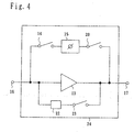
- variable gain amplifying apparatus 24 of this embodiment is shown in FIG. 4.
- the variable gain amplifying apparatus 24 is used as, for example, the variable gain amplifying apparatus 4 of the cellular phone terminal of FIG. 21. Furthermore, the parts identical to those of the first embodiment are given same symbols and descriptions thereof are not presented here.
- the variable gain amplifying apparatus 24 is comprised of the amplifier 13, the switching element 14, the phase shifter 15, the switching element 20, a feedback circuit 22 and a switching element 23.
- the amplifier 13 has its input connected to the input terminal 16 and its output connected to the output terminal 17.
- the switching element 14 is connected at one end to the input of the amplifier 13, and connected at the other end to one end of the phase shifter 15.
- the other end of the phase shifter 15 is connected to one end of the switching element 20, and the other end of the switching element 20 is connected to the output of the amplifier 13.
- One end of the switching element 23 is connected to the output of the amplifier 13, the other end of the switching element 23 is connected to one end of the feedback circuit 22, and the other end of the feedback circuit 22 is connected to the input of the amplifier 12.
- variable gain amplifying apparatus 24 of this embodiment is operated by being controlled by being controlled in accordance with a control circuit (not shown) as in the case of the first embodiment.
- This control circuit controls the operation of the variable gain amplifying apparatus 18 depending on the level of the receive signal received at the antenna 1.
- control is performed so that the switching elements 14 and 20 are enabled if the level of the input signal is higher than a predetermined level, and the switching elements 14 and 20 are disabled if the level of the input signal is equal to or lower than the predetermined level.
- Control is performed so that the amplifier 13 does not operate when the switching element 14 is enabled, and the amplifier 13 operates when the switching element 14 is disabled.
- This control is performed by, for example, supplying a power voltage for operating the amplifier 13 when the amplifier 13 is to be operated, and stopping the supply of a power voltage for operating the amplifier 13 when the operation of the amplifier 13 is to be stopped.
- the switching element 23 is disabled when the switching elements 14 and 20 are enabled, and the switching element 23 is enabled when the switching elements 14 and 20 are disabled.
- variable gain amplifying apparatus 24 operates in the low gain mode. That is, since the switching elements 14 and 20 are enabled, and the amplifier 13 stops operating, and the switching element 23 is disabled, the receive signal is inputted from the input terminal 16, passed through the switching element 14, the phase shifter 15 and the switching element 20, and outputted from the output terminal 17.
- variable gain amplifying apparatus 18 operates in the high gain mode, That is, since the switching elements 14 and 20 are disabled, and the amplifier 13 operates, and the switching element 23 is enabled, the receive signal is inputted from the input terminal 16, amplified by the amplifier 13, and outputted from the output terminal 17, and for some output signals from the amplifier 13, a negative feedback is applied to the input of the amplifier 13 via the switching element 23 and the feedback circuit 22.
- the phase shifter 15 shifts the phase of the receive signal inputted to the phase shifter 15 so that the amount of phase shift of the receive signal when the receive signal is passed through the amplifier 13 is substantially equal to the amount of phase shift of the receive signal when the receive signal is passed through the switching element 14, the phase shifter 15 and the switching element 20.
- variable gain amplifying apparatus 24 is switched from the high gain mode to the low gain mode, or switched from the low gain mode to the high gain mode, the phase of the signal outputted from the output terminal 17 is not shifted in a discontinuous manner.
- variable gain amplifying apparatus 24 of this embodiment in the pre-amplifier of the reception apparatus in the radio system represented by cellular phones, cellular phone terminals and the like with high quality of received voice can be provided.
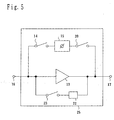
- variable gain amplifying apparatus 25 in which the positions of the switching element 23 and the feedback circuit 22 in the variable gain amplifying apparatus 24 of FIG. 4 are changed to each other is shown in FIG. 5. That is, in the variable gain amplifying apparatus 25, one end of the switching element 23 is connected to the input of the amplifier 13, the other end of the switching element 23 is connected to one end of the feedback circuit 22, and the other end of the feedback circuit 22 is connected to the output of the amplifier 13.
- Use of the variable gain amplifying apparatus 25 makes it possible to attain a same degree of effectiveness as that of this embodiment.
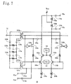
- FIG. 6 is a circuit diagram of a variable gain amplifying apparatus 30 of this embodiment.
- an input terminal P1 is connected to one end of an input side capacitor 131 for breaking direct currents, and the other end of the input side capacitor 131 is connected to one end of a switching element 121 and the base of a transistor 101.
- a bias power circuit 107 is connected to the base of the transistor 101, the emitter of the transistor 101 is grounded through an inductor 103 for widening the input dynamic range, and the collector of the transistor 101 is connected to the emitter of a transistor 102.
- the base of the transistor 102 is connected to a bias power circuit 108 and a bypass capacitor 106 which is grounded.
- the collector of the transistor 102 is connected to one end of an output side capacitor 133 for breaking direct currents and one end of a negative feedback side capacitor 105 for breaking direct currents, and the collector of the transistor 102 is also connected to a power supply terminal for amplifiers Vcc through a choke coil 132 for high-frequency cutoff.
- the other end of the output side capacitor 133 is connected to an output terminal P2.
- the other end of the negative feedback side capacitor 105 is connected to one end of a switching element 123 and one end of switching element 122.
- the other end of the switching element 123 is connected to one end of a resistor 104 to apply a negative feedback, and the other end of the resistor 104 is connected to the base of the transistor 101.
- the other end of the switching element 122 is connected to one end of a capacitor 116, and the other end of the capacitor 116 is connected to a grounded resistor 113 and one end of a capacitor 115.
- the other end of the capacitor 115 is connected to a grounded resistor 112 and one end of a capacitor 114.
- the other end of the capacitor 114 is connected to a grounded resistor 111 and the other end of the switching element 121.
- a switching element power supply terminal 31 is connected to a terminal for control of the switching element 121 and the switching element 122.
- the switching element power supply terminal 31 is connected to one end of an inverter 124, and the other end of the inverter 124 is connected to a terminal for control of the switching element 123.
- variable gain amplifying apparatus 30 of this embodiment corresponds to the variable gain amplifying apparatus 24 of the second embodiment of FIG. 4.
- the input terminal P1 corresponds to the input terminal 16 of FIG. 4
- the terminal P2 corresponds to the output terminal 17 of FIG. 4
- the resistor 104 corresponds to the feedback circuit 22 of FIG. 4
- the inverter 124 and the switching element 123 correspond to the switching element 23 of FIG. 4
- the transistors 101 and 102, the capacitor 106, the inductor 103, and the bias power circuits 107 and 108 correspond to the amplifier 13 of FIG. 4.
- the capacitors 114, 115 and 116 and the resistors 111, 112 and 113 correspond to the phase shifter 15 of FIG. 4
- the switching element 121 corresponds to the switching element 14 of FIG. 4
- the switching element 122 corresponds to the switching element 20 of FIG. 4.
- the switching element power supply terminal 31 is a terminal to supply a power voltage for changing the states of the switching elements 121, 122 and 123 from the enabled state to the disabled state and vice versa.
- the bias power circuit 107 is a circuit to supply a bias voltage to the base of the transistor 101
- the bias power circuit 108 is a circuit to supply a bias voltage to the base of the transistor 102, and is capable of stopping and starting the supply of operating voltage by means of a control circuit (not shown).
- the power supply terminal for amplifiers Vcc is a terminal to supply operating voltage to the transistors 102 and 101.
- the switching element power supply terminal 21 is a terminal to change the states of the switching elements 121, 122 and 123 from the enabled state to the disabled state and vice versa by supplying a control power voltage or stopping the supply of the power voltage to the respective control terminals for the switching elements 121, 122 and 123.
- terminals of this embodiment such as the input terminal P1 and the output terminal P2 also include terminals such as pad electrodes and modes as junction points of elements in the wiring.
- the resistors 111, 112 and 113 and the like are made of polysilicon, and the capacitors 114, 115 and 116 and the like are composed of MOS capacitors. Furthermore, the capacitors 114, 115 and 116 may be composed of MIM capacitors.
- the receive signal is amplified by elements such as the transistors 101 and 102, but these elements, namely the elements corresponding to the amplifier 13 of FIG. 4 cause the phase of the receive signal outputted from the output terminal P2 to be advanced farther than the phase of the receive signal inputted to the input terminal P1.
- the input impedance to the base of the transistor 101 is smaller than the output impedance of the collector of the transistor 102.
- variable gain amplifying apparatus 30 operating in the high gain mode will be described.
- the variable gain amplifying apparatus 30 When the level of the receive signal inputted from the input terminal P1 is equal to or lower than a predetermined level, the variable gain amplifying apparatus 30 operates in the high gain mode. That is, when detecting that the level of the receive signal is lower than the predetermined level, the control circuit (not shown) supplies a voltage (e.g. voltage of 0V) allowing the switching elements 122 and 121 to become disabled as a control voltage that is supplied to the switching element power supply terminal 31. The control circuit (not shown) supplies a voltage allowing the transistors 101 and 102 to operate from the bias circuits 107 and 108. Thus, the transistors 101 and 102 become enabled.
- a voltage e.g. voltage of 0V
- the receive signal inputted from the input terminal P1 is passed through the input side capacitor 131 and then inputted to the base of the transistor 101.
- the receive signal is not flown to the capacitor 114 because the switching element 121 is disabled.
- the base of the transistor 101 is supplied with a bias voltage by the bias power circuit 107, and the base of the transistor 102 is supplied with a bias voltage by the bias power circuit 108.
- the receive signal inputted to the base of the transistor 101 is amplified by the transistors 101 and 102 and then outputted from the collector of the transistor 102.
- Some of signals outputted from the collector of the transistor 102 are passed through the capacitor 133 and then outputted from the output terminal P2 to the rear stage such as the mixer 7 .
- the other signals outputted from the collector of the transistor 102 are passed through the negative feedback side capacitor 105.
- the signal passed through the negative feedback side capacitor 105 is passed through the switching element 123, adjusted to a predetermined level in the resistor 104, and again inputted to the base of the transistor 101.
- the signal passed through the negative feedback side capacitor 105 is not flown to the capacitor 116 because the switching element 122 is disabled.
- the receive signal inputted from the input terminal P1 is amplified in the transistors 101, 102 while receiving a negative feedback, and is then outputted from the output terminal P2 to the rear stage.
- the phase of the receive signal outputted from the output terminal P2 is advanced farther than the phase of the receive signal inputted from the input signal P1, and the input impedance
- Zi(high) and Zo(high) are both complex numbers.
- variable gain amplifying apparatus 30 operating in the low gain mode
- variable gain amplifying apparatus 30 When the level of the receive signal inputted from the input terminal P1 is higher than a predetermined level, the variable gain amplifying apparatus 30 operates in the low gain mode. That is, when detecting that the level of the receive signal is higher than the predetermined level, the control circuit (not shown) turns to the low gain mode in order to prevent the situation in which the transistors 101 and 102 are saturated.
- the control circuit when detecting that the level of the receive signal is higher than the predetermined level, the control circuit (not shown) supplies a voltage (e.g. voltage of 3V) allowing the switching elements 122 and 121 to become enabled as a control voltage that is supplied to the switching element power supply terminal 31.
- the control circuit stops supplying a voltage allowing the transistors 101 and 102 from the power supply terminal for amplifiers Vcc. Thus, the transistors 101 and 102 stop their operations.
- the receive signal inputted from the input terminal P1 is passed through the input side capacitor 131, the switching element 121, the capacitors 114, 115 and 116, and a circuit portion consisting of the capacitors 114, 115 and 116 and resistors 111, 112 and 113.
- This circuit portion functions as the phase shifter 15 of FIG. 4 as described above. An adjustment is made so that the phase of the receive signal inputted from the input terminal P1 is advanced in this circuit portion.
- the ratio between the resistance value of the resistor 111 and the resistance value of the resistor 112 and the resistance value of the resistor 113 is 1:a:a 2 .
- the ratio between the capacitance value of the capacitor 114 and the capacitance value of the capacitor 115 and the capacitance value of the capacitor 116 is a 2 :a:1.
- an adjustment is made so that a represents a predetermined value greater than 1.
- the circuit portion functioning as the phase shifter 15 of FIG. 4 has basic unit circuits each consisting of a resistor and a capacitor combined in three stages.
- the circuit portion functioning as the phase shifter 15 of FIG. 4 also plays a role as an impedance converter.
- the output impedance of this circuit may be expressed as a
- Z1 is a complex number.
- the input impedance of a circuit being the second-stage basic unit circuit that consists of the resistor 112 and the capacitor 115 equals a
- the input impedance of a circuit being the third-stage basic unit circuit that consists of the resistor 113 and the capacitor 116 equals a 2
- the value of the output impedance of the basic unit circuit in a certain stage is relatively close to the value of the output impedance of the basic unit in the following stage, and thus a loss between the stages is reduced.
- the frequency properties of passing phases between stages are relatively close to each other.
- the input impedance of the base of the transistor 101 equals
- the output impedance of the collector of the transistor 102 equals
- the impedances Z1 and Zi(high) are made to be close to each other, whereby the value of output impedance in the high gain mode is relatively close to the value of output impedance in the low gain mode.
- the passing phase of the circuit portion functioning as the phase shifter 15 of FIG. 4 is uniquely determined, the value of passing phase is made to be close to the value of passing phase in the high gain mode by increasing/decreasing the number of stages of basic unit circuits consisting of resistors and capacitors.
- the circuit portion functioning as the phase shifter 15 of FIG. 4 is constituted by n basic unit circuits (n is an integer number greater than 1)
- the value of a is defined as a value satisfying the following equation 12. [Equation 12]
- a n
- a receive signal is outputted from the output terminal P2 as a signal of which amount of phase advance is substantially equal to the amount of advance of the passing phase in the case of high gain mode.
- the signal passed through this circuit portion is passed through the switching element 122. Because the switching element 124 is disabled, this signal is not flown to the resistor 104. Thus, the signal passed through the switching element 122 is passed through the negative feedback side capacitor 105 and then outputted from the output terminal P2 through the output side capacitor 133.
- the phase of a passing signal is adjusted in the portion corresponding to the phase shifter 15 of FIG. 4, and therefore even if the variable gain amplifying apparatus is switched from the high gain mode to the low gain mode, the situation in which the phase of the signal outputted from the output terminal P2 is shifted in a discontinuous manner can be sufficiently alleviated.
- variable gain amplifying apparatus 30 of this embodiment may have a configuration in which a resistor 2641 is inserted between the switching element 122 and the ground, a resistor 2642 is inserted between the switching element 123 and the ground, and a capacitor 2643 is inserted between the base of the transistor 101 and the resistor 104, as shown in FIG. 26.
- the switching elements 121, 122 and 123 take on 0 potentials at least at one ends, and therefore the switching elements are reliably enabled/disabled, and the insertion loss when the switching elements are enabled is improved.
- Inductor quarter wave lines may be used instead of the resistors 2641, 2642.
- variable gain amplifying apparatus 30 of this embodiment has been described as an unbalanced circuit, but may also be achieved as a balanced circuit.
- variable gain amplifying apparatus 32 achieved as a balanced circuit by modifying the variable gain amplifying apparatus 30 of this embodiment is shown in FIG. 7.
- the input terminal P1 of FIG. 6 is replaced by input terminals P1a and P1b in FIG. 7, the input side capacitor 131 of FIG. 6 is replaced by input side capacitors 131a, 131b in FIG. 7, the switching element 121 of FIG. 6 is replaced by switching elements 121a, 121b in FIG. 7, the transistor 101 of FIG. 6 is replaced by transistors 101a, 101b in FIG. 7, the transistor 102 of FIG. 6 is replaced by transistors 102a, 102b in FIG. 7, the inductor 103 of FIG. 6 is replaced by inductors 103a, 103b in FIG. 7, the resistor 104 of FIG. 6 is replaced by resistors 104a, 104b in FIG. 7, the output side capacitor 133 of FIG.
- variable gain amplifying apparatus 32 may also have a configuration in which the switching elements 121, 122, 123a and 123b take on 0 potentials at least at one ends as in the case of the variable gain amplifying apparatus 30.
- the switching elements are reliably enabled/disabled, and the insertion loss when the switching elements are enabled is improved.
- variable gain amplifying apparatus 30 of this embodiment may be achieved as a balanced circuit like the variable gain amplifying apparatus 32, for example.
- variable gain amplifying apparatus 30 of FIG. 6 when the variable gain amplifying apparatus is used in the high gain mode, the receive signal is passed through the circuit portion corresponding to the amplifier 13 of FIG. 4, whereby the phase of the receive signal outputted from the output terminal P2 is advanced farther than the phase of the receive signal inputted to the input terminal P1, and the input impedance to the base of the transistor 101 is smaller than the output impedance of the collector of the transistor 102, but the circuit portion corresponding to the phase shifter 15 of FIG. 4 should be changed if the circuit portion corresponding to the amplifier 13 of FIG. 4 has a characteristic other than that described above.
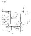
- FIG. 8 a circuit diagram of a variable gain amplifying apparatus 33 in which the circuit portion corresponding to the phase shifter 15 is changed is shown in FIG. 8.
- the passing phase in the high gain mode is advanced, and the input impedance of the portion corresponding to the amplifier 13 is larger than the output impedance of the same portion.
- one end of a capacitor 314 is connected to one end of the switching element 121, and the other end of the capacitor 314 is connected to a grounded resistor 311 and to one end of a capacitor 315.
- the other end of the capacitor 315 is connected to a grounded resistor 312 and to one end of a capacitor 316.
- the other end of the capacitor 316 is connected to a grounded resistor 313 and to one end of the switching element 122.
- the circuit portion functioning as the phase shifter 15 of FIG. 4 in the variable gain amplifying apparatus 33 adjusts the phase in the same way as the third embodiment.
- the ratio between the resistance value of the resistor 311 and the resistance value of the resistor 312 and the resistance value of the resistor 313 is 1:a:a 2 .
- the ratio between the capacitance value of the capacitor 314 and the capacitance value of the capacitor 315 and the capacitance value of the capacitor 316 is a 2 :a:1.
- an adjustment is made so that the value of a equals a predetermined value smaller than 1. That is, the value of a is previously designed so as to provide an amount of phase advance equal to the amount of advance of the phase of the receive signal outputted from the output terminal P2 relative to the phase of the receive signal inputted from the input terminal P1 in the case of high gain mode.
- the value of the value of a can be determined in the same way as described above.
- variable gain amplifying apparatus 33 of this embodiment may have a configuration in which the switching elements 121, 122, 123 take on 0 potentials at least at one ends as in the case of the variable gain amplifying apparatus 30 of this embodiment. Thereby, the switching elements are reliably enabled/disabled, and the insertion loss when the switching elements are enabled is improved.
- variable gain amplifying apparatus 33 of this embodiment may also be comprised of balanced circuits as described in this embodiment.
- FIG. 9 A circuit diagram of another variable gain amplifying apparatus 34 in which the circuit portion corresponding to the phase shifter 15 is changed is shown in FIG. 9.
- the passing phase of the receive signal is delayed in the case of high gain mode, and the input impedance of the portion corresponding to the amplifier 13 is smaller than the output impedance of the same portion.
- one end of a resistor 414 is connected to one end of the switching element 121, a grounded capacitor 411 is connected to one end of the resistor 414, and the other end of the resistor 414 is connected to one end of a resistor 415 and to a grounded capacitor 412.
- a grounded capacitor 413 is connected to the other end of the resistor 415, and the other end of the resistor 415 is connected to one end of a resistor 416.
- the other end of the resistor 416 is connected to one end of the switching element 122.
- the circuit portion functioning as the phase shifter 15 of FIG. 4 has the phase adjusted in the same way as this embodiment.
- the ratio between the resistance value of the resistor 414 and the resistance value of the resistor 415 and the resistance value of the resistor 416 is 1:a:a 2 .
- the ratio between the capacitance value of the capacitor 411 and the capacitance value of the capacitor 412 and the capacitance value of the capacitor 413 is a 2 :a:1.
- an adjustment is made so that the value of a equals a predetermined value smaller than 1. That is, the value of a is previously designed so as to provide an amount of phase delay equal to the amount of delay of the phase of the receive signal outputted from the output terminal P2 relative to the phase of the receive signal inputted from the input terminal P1 in the case of high gain mode.
- the value of the value of a can be determined in the same way as described above.
- variable gain amplifying apparatus 34 of this embodiment may have a configuration in which the switching elements 121, 122, 123 take on 0 potentials at least at one ends as in the case of the variable gain amplifying apparatus 30 of this embodiment. Thereby, the switching elements are reliably enabled/disabled, and the insertion loss when the switching elements are enabled is improved.
- variable gain amplifying apparatus 34 of this embodiment may also be comprised of balanced circuits as described in this embodiment.
- FIG. 10 A circuit diagram of another variable gain amplifying apparatus 35 in which the circuit portion corresponding to the phase shifter 15 is changed is shown in FIG. 10.
- the passing phase of the receive signal is delayed in the case of high gain mode , and the input impedance of the portion corresponding to the amplifier 13 is larger than the output impedance of the same portion.
- one end of a resistor 514 is connected to one end of the switching element 121, and a grounded capacitor 511 is connected to the other end of the resistor 514, and one end of a resistor 515 is connected to the other end of the resistor 514.
- a grounded capacitor 512 is connected to the other end of the resistor 515, and the other end of the resistor 515 is connected to one end of a resistor 516.
- a grounded capacitor 513 is connected to the other end of the resistor 516, and one end of the switching element 122 is connected to the other end of the resistor 516.
- the circuit portion functioning as the phase shifter 15 of FIG. 4 has the phase adjusted in the same way as this embodiment.
- the ratio between the resistance value of the resistor 514 and the resistance value of the resistor 515 and the resistance value of the resistor 516 is 1:a:a 2 .
- the ratio between the capacitance value of the capacitor 511 and the capacitance value of the capacitor 512 and the capacitance value of the capacitor 513 is a 2 :a:1.
- an adjustment is made so that the value of a equals a predetermined value smaller than 1. That is, the value of a is previously designed so as to provide an amount of phase delay equal to the amount of delay of the phase of the receive signal outputted from the output terminal P2 relative to the phase of the receive signal inputted from the input terminal P1 in the case of high gain mode.
- the value of the value of a can be determined in the same way as described above.
- variable gain amplifying apparatus 35 of this embodiment may have a configuration in which the switching elements 121, 122, 123 take on 0 potentials at least at one ends as in the case of the variable gain amplifying apparatus 30 of this embodiment. Thereby, the switching elements are reliably enabled/disabled, and the insertion loss when the switching elements are enabled is improved.
- variable gain amplifying apparatus 35 may also be comprised of balanced circuits as described in this embodiment.
- a FET switch made of potassium and arsenic a MOSFET switch of triple-well structure and a switch of silicon-on-insulator structure, and the like may be used.
- FIG. 11 schematically shows the cross sectional structure of a high frequency switching element 50 for use in the switching elements 121, 122 and 123. That is, the high frequency switching element is a MOSFET switch of triple-well structure.
- the high frequency switching element 50 is formed on an element formation area partitioned by trench portions 608, 609 selectively provided on a semiconductor substrate 601 made of P-type silicon, for example.
- a n-type well 602 and a p-type well 603 surrounded by the n-type well 602 are formed on the element formation area in the semiconductor substrate 601.
- a drain layer 606 and a source layer 607 are formed on the p-type well 603 with some distance therebetween, and a gate electrode 605 made of polysilicon is formed via a gate insulation film 604 made of silicon oxide in the area between the drain layer 606 and the source layer 607 on the p-type well 603.
- the drain layer 606 is connected to an input node P10 receiving the receive signal inputted from the input side capacitor 11 of FIG. 6, and the source layer 607 is connected to an output node P20 outputting the receive signal to the capacitor 114 and resistor 111 shown in FIG. 6.
- the gate electrode 605 is connected to a voltage control terminal P3 receiving a control voltage supplied from the switching element power supply terminal 31 through a resistor 611, and a n-type well 602 is connected to voltage control terminal P3 through a resistor 610.
- the semiconductor substrate 601 is grounded, and the p-type well 603 is grounded through a resistor 612.
- a reverse bias voltage is applied to between the n-type well 602 and the p-type well 603, resulting in a depletion layer by pn connection composed of the interface between the n-type well 602 and the p-type well 603, and thus the n-type well 602 and the p-type well 603 are insulated from each other in the vertical direction relative to the substrate surface.
- a reverse voltage is applied to between the semiconductor substrate 601 and the n-type well 602, resulting in a depletion layer by pn connection composed of the interface between the semiconductor substrate 601 and the n-type well 602, and thus the semiconductor substrate 601 and the n-type well 602 are insulated from each other.
- the high frequency switching element 50 when the high frequency switching element 50 is enabled, the level of losses of the receive signal due to the situation in which the receive signal inputted to the input node P10 leaks into the semiconductor substrate 601 from the drain layer 606, the source layer 607 and the channel area formed between the drain layer 606 and the source layer 607 can be reduced, and as a result, the level of insertion losses by the high frequency element 50 during operation in the low gain mode can be reduced.
- the level of leakage into the semiconductor substrate 601 of the receive signal inputted to the input node P10 through the drain layer 606 can be reduced even when the high frequency switching element 50 is disabled.
- degradation of noise characteristics due to the fact that some of high frequency signals inputted to the input terminal P1 shown in FIG. 6 bring about insertion losses of the high frequency switching element 50 can be alleviated during operation in the high gain mode.
- inductance elements may be used instead of resistors 610, 611 and 612.
- FIG. 12 A circuit diagram of a variable gain amplifying apparatus 36 of the fourth embodiment is shown in FIG. 12.
- the portion corresponding to the phase shifter 15 of FIG. 4 is constituted by strip lines.
- variable gain amplifying apparatus 36 of the fourth embodiment the passing phase of the receive signal in the case of the high gain mode is delayed, and the input impedance of the portion corresponding to the amplifier 13 is smaller than the output impedance of the same portion.
- variable gain amplifying apparatus 36 is different from the variable gain amplifying apparatus 33 in the portion corresponding to the phase shifter 15 of FIG. 4.
- the portion corresponding to the phase shifter 15 of FIG. 4 is comprised of strip lines 711, 712, 713.
- One of the strip line 711 is connected to one of the switching element 121, the other end of the strip line 711 is connected to one end of the strip line 712, and the other end of the strip line 712 is connected to one end of the strip line 713.
- the other end of the strip line 713 is connected to the switching element 122.
- strip lines 711, 712, 713 are each made of aluminum wire.
- the strip limes 711, 712, 713 may be made of copper wire or gold wire.
- the circuit portion functioning as the phase shifter 15 of FIG. 4 adjusts the phase in the same way as the third embodiment.
- the ratio between the impedance value of the strip line 711 and the impedance value of the strip line 712 and the impedance value of the strip line 713 is 1:a:a 2 .
- an adjustment is made so that the value of a equals a predetermined value larger than 1. That is, the value of a is previously designed so as to provide an amount of phase delay equal to the amount of delay of the phase of the receive signal outputted from the output terminal P2 relative to the phase of the receive signal inputted from the input terminal P1 in the case of high gain mode.
- the circuit portion functioning as the phase shifter 15 of FIG. 4 has basic unit circuits, namely strip lines combined in three stages.
- the circuit portion functioning as the phase shifter 15 of FIG. 4 also plays a role as an impedance converter.
- the impedance of the strip line 711 being a first-stage basic unit circuit equals Z1
- the input impedance of the base of the transistor 101 in the case of the high gain mode equals
- the value of Z1 is selected so that the values of Z1 and
- the impedance of the strip line 713 being a third-stage basic unit circuit equals Z3, and the output impedance of the collector of the transistor 102 equals
- the value of Z1 is selected so that the input impedance in the case of high gain mode is close to the input impedance in the case of low gain mode
- the value of Z3 is selected so that the output impedance in the case of high gain mode is close to the output impedance in the case of low gain mode.
- the circuit portion functioning as the phase shifter 15 of FIG. 4 is constituted by one strip line with its line width continuously changed, and the impedance of the input side of the strip line is given the value of Z1 when the circuit portion has basic unit circuits combined in three stages, and the impedance of the output side of the strip line is given the value of Z3 when the circuit portion has basic unit circuits combined in three stages.
- Phase adjustment can be achieved by changing the overall length of the strip line.
- strip lines 711, 712 and 713 are formed as micro strip lines
- the impedances of strip lines 711, 712 and 713 can be determined in the same way as the above strip lines 711, 712 and 713 by pursuing the following procedure.
- a micro strip line 82 constituting a basic unit circuit is shown in FIG. 24.
- the micro strip line 82 is formed on a dielectric 81, and no dielectric is formed on the side opposite to the dielectric 81 in the micro strip line 82.
- the width of the micro strip line 82 is w
- the height of the dielectric 81 is h
- the permittivity of the dielectric 81 is ⁇ r .
- the impedance Z 0 of the strip line 82 can be approximated as is found in the following equation 17.
- the impedance is changed using the strip lines 711, 712 and 713 having different line widths, but the impedance may be changed using dielectrics of different relative permittivities or different thicknesses.
- strip lines 711, 712 and 713 instead of the strip lines 711, 712 and 713, a line having a taper in which characteristic impedance varies in the range of from Z1 to Z4 may be used.
- variable gain amplifying apparatus 36 of this embodiment may have a configuration in which the switching elements 121, 122, 123 take on 0 potentials at least at one ends as in the case of the variable gain amplifying apparatus 30 of the third embodiment.
- the switching elements are reliably enabled/disabled, and the insertion loss when the switching elements are enabled is improved.
- variable gain amplifying apparatus 36 may also be comprised of balanced circuits as described in the third embodiment.
- variable gain amplifying apparatus 37 of FIG. 13 the passing phase of the receive signal in the case of high gain mode is delayed, and the input impedance of the portion corresponding to the amplifier 13 is larger than the output impedance of the same portion.
- the portion corresponding to the phase shifter 15 of FIG. 4 is comprised of strip lines 811, 812, 813.
- One end of the strip line 811 is connected to one end of the switching element 121, the other end of the strip line 811 is connected to one end of the strip line 812, and the other end of the strip line 812 is connected to one end of the strip line 813.
- the other end of the strip line 813 is connected to the switching element 122.
- This circuit portion adjusts the phase in the same way as the third embodiment.
- the ratio between the impedance value of the strip line 811 and the impedance value of the strip line 812 and the impedance value of the strip line 813 is 1:a:a 2 .
- an adjustment is made so that the value of a equals a predetermined value smaller than 1. That is, the value of a is previously designed so as to provide an amount of phase delay equal to the amount of delay of the phase of the receive signal outputted from the output terminal P2 relative to the phase of the receive signal inputted from the input terminal P1 in the case of high gain mode.
- the value of a can be determined in the same way as described above.
- strip lines 811, 812 and 813 instead of the strip lines 811, 812 and 813, a line having a taper in which characteristic impedance varies in the range of from Z1 to Z4 may be used.
- variable gain amplifying apparatus 37 of this embodiment may have a configuration in which the switching elements 121, 122, 123 take on 0 potentials at least at one ends as in the case of the variable gain amplifying apparatus 30 of the third embodiment.
- the switching elements are reliably enabled/disabled, and the insertion loss when the switching elements are enabled is improved.
- variable gain amplifying apparatus 37 may also be comprised of balanced circuits as described in the third embodiment.
- FIG. 14 A circuit diagram of a variable gain amplifying apparatus 38 of the fifth embodiment is shown in FIG. 14.
- the portion corresponding to the phase shifter 15 of FIG. 4 is constituted by parallel twin lines.
- variable gain amplifying apparatus 38 is a variable gain amplifying apparatus in which the portion corresponding to the phase shifter 15 of the balanced variable gain amplifying apparatus 32 of the third embodiment is replaced by parallel twin lines.
- variable gain amplifying apparatus 38 of this embodiment has balanced circuits.
- variable gain amplifying apparatus 38 For the variable gain amplifying apparatus 38, the passing phase of the receive signal in the case of high gain mode is delayed, and the input impedance of the portion corresponding to the amplifier 13 is smaller than the output impedance of the same portion.
- the portion corresponding to the phase shifter 15 of FIG. 4 in the variable gain amplifying apparatus 38 is comprised of parallel twin lines 911a, 911b, parallel twin lines 912a, 912b, and parallel twin lines 913a, 913b.
- One ends of the parallel twin lines 911a and 911b are connected to the switching elements 121a and 121b, respectively, and the other ends of the parallel twin lines 911a and 911a are connected to one ends of the parallel twin lines 912a and 912b, respectively.
- the other ends of the parallel twin lines 912a and 912b are connected to one ends of the parallel twin lines 913a and 913b, respectively.
- the other ends of the parallel twin lines 913a and 913b are connected to the switching elements 122a and 122b, respectively.
- the parallel twin lines 911a, 911b, the parallel twin lines 912a, 912b, and the parallel twin lines 913a, 913b are each made of aluminum wire. Furthermore, the parallel twin lines 911a, 911b, the parallel twin lines 912a, 912b, and the parallel twin lines 913a, 913b may be made of copper wire or gold wire.
- the circuit portion functioning as the phase shifter 15 of FIG. 4 adjusts the phase in the same way as the third embodiment.
- the ratio between the distance between the parallel twin lines 911a and 911b and the distance between the parallel twin lines 912a and 912b and the distance between the parallel twin lines 913a and 913b is 1:a:a 2 .
- an adjustment is made so that the value of a equals a predetermined value smaller than 1. That is, the value of a is previously designed so as to provide amounts of phase delay equal to the amounts of delay of the phases of the receive signals outputted from output terminals P2a and P2b relative to the phases of the receive signals inputted from input terminals P1a and P1b in the case of high gain mode.
- input/output impedances are determined depending on the line width, and therefore the value of a can be determined in the same way as the strip line described in the fourth embodiment.
- signals of which amounts of phase delay are substantially equal to the amount of delay of the passing phase in the case of high gain mode are outputted from the output terminals P2a and P2b.
- variable gain amplifying apparatus 38 of this embodiment may have a configuration in which the switching elements 121, 122, 123 take on 0 potentials at least at one ends as in the case of the variable gain amplifying apparatus 30 of the third embodiment. Thereby, the switching elements are reliably enabled/disabled, and the insertion loss when the switching elements are enabled is improved.
- variable gain amplifying apparatus 39 of FIG. 15 the passing phase of the receive signal in the case of high gain mode is delayed, and the input impedance of the portion corresponding to the amplifier 13 of FIG. 4 is larger than the output impedance of the same portion.
- the portion corresponding to the phase shifter 15 of FIG. 4 in the variable gain amplifying apparatus 39 is comprised of parallel twin lines 1011a, 1011b, parallel twin lines 1012a, 1012b, and parallel twin lines 1013a, 1013b.
- One ends of the parallel twin lines 1011a and 1011b are connected to the switching elements 121a and 121b, respectively, and the other ends of the parallel twin lines 1011a and 1011a are connected to one ends of the parallel twin lines 1012a and 1012b, respectively.
- the other ends of the parallel twin lines 1012a and 1012b are connected to one ends of the parallel twin lines 1013a and 1013b, respectively.
- the other ends of the parallel twin lines 1013a and 1013b are connected to the switching elements 122a and 122b, respectively.
- This circuit portion adjusts the phase in the same way as the third embodiment.
- the ratio between the distance between the parallel twin lines 1011a and 1011b and the distance between the parallel twin lines 1012a and 1012b and the distance between the parallel twin lines 1013a and 1013b is 1:a:a 2 .
- an adjustment is made so that the value of a equals a predetermined value larger than 1. That is, the value of a is previously designed so as to provide amounts of phase delay equal to the amounts of delay of the phases of the receive signals outputted from output terminals P2a and P2b relative to the phases of the receive signals inputted from input terminals P1a and P1b in the case of high gain mode.
- input/output impedances are determined depending on the line width, and therefore the value of a can be determined in the same way as the strip line described in the fourth embodiment.
- signals of which amounts of phase delay are substantially equal to the amount of delay of the passing phase in the case of high gain mode are outputted from the output terminals P2a and P2b.
- variable gain amplifying apparatus 39 of this embodiment may have a configuration in which the switching elements 121, 122, 123 take on 0 potentials at least at one ends as in the case of the variable gain amplifying apparatus 30 of the third embodiment. Thereby, the switching elements are reliably enabled/disabled, and the insertion loss when the switching elements are enabled is improved.
- FIG. 16 A circuit diagram of a variable gain amplifying apparatus 40 of the sixth embodiment is shown in FIG. 16.
- the portion corresponding to the phase shifter 15 of FIG. 4 is constituted by capacitors and inductors.
- variable gain amplifying apparatus 40 of this embodiment the passing phase of the receive signal in the case of high mode is advanced, and the input impedance of the portion corresponding to the amplifier 13 is smaller than the output impedance of the same portion.
- variable gain amplifying apparatus 40 is different from the variable gain amplifying apparatus 33 in the portion corresponding to the phase shifter 15 of FIG. 4.
- the portion corresponding to the phase shifter 15 of FIG. 4 is comprised of capacitors 1114, 1115, 1116 and inductors 1111, 1112, 1113.
- the passing phase of the receive signal in the case of high gain mode is advanced, and the input impedance of the portion corresponding to the amplifier 13 is smaller than the output impedance of the same portion.
- one end of the capacitor 1114 is connected to one end of the switching element 121, and the grounded inductor 1111 is connected to one end of the capacitor 1114.
- the other end of the capacitor 1114 is connected to the grounded inductor 1112 and to one end of the capacitor 1115.
- the other end of the capacitor 1115 is connected to the grounded inductor 1112 and to one end of the capacitor 1116.
- One end of the switching element 122 is connected to the other end of the capacitor 1116.
- the inductors 1111, 1112, 1113 are made of aluminum wire
- the capacitors 1114, 1115, 1116 are composed of MOS capacitors
- the wiring connecting the capacitor to the inductor is made of gold wire
- the inductors 1111, 1112, 1113 may be made of copper wire
- the capacitors 1114, 1115, 1116 may be composed of MIM capacitors.
- the circuit portion functioning as the phase shifter 15 of FIG. 4 in the variable gain amplifying apparatus 40 adjusts the phase in the same way as the third embodiment.
- the ratio between the inductance value of the inductor 1111 and the inductance value of the inductor 1112 and the inductance value of the inductor 1113 is 1:a:a 2 .
- the ratio between the capacitance value of the capacitor 1114 and the capacitance value of the capacitor 1115 and the capacitance value of the capacitor 1116 is a 2 :a:1.
- an adjustment is made so that the value of a equals a predetermined value larger than 1. That is, the value of a is previously adjusted so as to provide an amount of phase advance equal to the amount of advance of the phase of the receive signal outputted from the output terminal P2 relative to the phase of the receive signal inputted from the input terminal P1 in the case of high gain mode.
- the value of a is determined in the same way as the method of the determining the value of a described in the third embodiment except that the resistor is replaced by the inductor. Because the inductor is used in stead of the resistor of the third embodiment, the level of passing loss is reduced compared to the third embodiment.
- variable gain amplifying apparatus 40 of this embodiment may have a configuration in which the switching elements 121, 122, 123 take on 0 potentials at least at one ends as in the case of the variable gain amplifying apparatus 30 of the third embodiment. Thereby, the switching elements are reliably enabled/disabled, and the insertion loss when the switching elements are enabled is improved.
- variable gain amplifying apparatus 40 of this embodiment has been described as an unbalanced circuit, but may also be achieved as a balanced circuit.
- variable gain amplifying apparatus 41 achieved as a balanced circuit by modifying the variable gain amplifying apparatus 40 of this embodiment is shown in FIG. 17.
- variable gain amplifying apparatus 41 of FIG. 17 the portion corresponding to the phase shifter 15 of the variable gain amplifying apparatus 32 of the third embodiment is replaced by capacitors 1114a, 1114b, 1115a, 1115b, 1116a, 1116b, and inductors 1111, 1112, 1113.
- the variable gain amplifying apparatus 41 is same as the third embodiment.
- variable gain amplifying apparatus 41 having balanced circuits makes it possible to attain a same degree of effectiveness as that of this embodiment.
- variable gain amplifying apparatus 40 of FIG. 17 when the variable gain amplifying apparatus is used in the high gain mode, the receive signal is passed through the circuit portion corresponding to the amplifier 13 of FIG. 4, whereby the phase of the receive signal outputted from the output terminal P2 is advanced farther than the phase of the receive signal inputted to the input terminal P1, and the input impedance to the base of the transistor 101 is smaller than the output impedance of the collector of the transistor 102, but the circuit portion corresponding to the phase shifter 15 of FIG. 4 should be changed if the circuit portion corresponding to the amplifier 13 of FIG. 4 has a characteristic other than that described above.
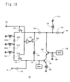
- FIG. 18 a circuit diagram of a variable gain amplifying apparatus 42 in which the circuit portion corresponding to the phase shifter 15 is changed is shown in FIG. 18.
- the passing phase in the high gain mode is advanced, and the input impedance of the portion corresponding to the amplifier 13 is larger than the output impedance of the same portion.
- one end of a capacitor 1314 is connected to one end of the switching element 121, and the other end of the capacitor 1314 is connected to a grounded inductor 1311 and to one end of a capacitor 1315.
- the other end of the capacitor 1315 is connected to a grounded inductor 1312 and to one end of a capacitor 1316.
- the other end of the capacitor 1316 is connected to a grounded inductor 1313 and to one end of the switching element 122.
- the circuit portion functioning as the phase shifter 15 of FIG. 4 in the variable gain amplifying apparatus 42 adjusts the phase in the same way as the third embodiment.
- the ratio between the inductance value of the inductor 1311 and the inductance value of the inductor 1312 and the inductance value of the inductor 1313 is 1:a:a 2 .
- the ratio between the capacitance value of the capacitor 1314 and the capacitance value of the capacitor 1315 and the capacitance value of the capacitor 1316 is a 2 :a:1.
- an adjustment is made so that the value of a equals a predetermined value smaller than 1. That is, the value of a is previously designed so as to provide an amount of phase advance equal to the amount of advance of the phase of the receive signal outputted from the output terminal P2 relative to the phase of the receive signal inputted from the input terminal P1 in the case of high gain mode.
- the value of a is determined in the same way as the method of the determining the value of a described in the third embodiment except that the resistor is replaced by the inductor. Because the inductor is used in stead of the resistor of the third embodiment, the level of passing loss is reduced compared to the third embodiment.
- variable gain amplifying apparatus 42 of this embodiment may have a configuration in which the switching elements 121, 122, 123 take on 0 potentials at least at one ends as in the case of the variable gain amplifying apparatus 30 of the third embodiment. Thereby, the switching elements are reliably enabled/disabled, and the insertion loss when the switching elements are enabled is improved.
- variable gain amplifying apparatus 42 of this embodiment may also be constituted by balanced circuits as described in this embodiment.
- FIG. 19 A circuit diagram of another variable gain amplifying apparatus 43 in which the circuit portion corresponding to the phase shifter 15 is changed is shown in FIG. 19.
- the passing phase of the receive signal is delayed in the case of high gain mode, and the input impedance of the portion corresponding to the amplifier 13 is smaller than the output impedance of the same portion.
- one end of an inductor 1414 is connected to one end of the switching element 121, a grounded capacitor 1411 is connected to one end of the inductor 1414, and the other end of the inductor 1414 is connected to one end of an inductor 1415 and to a grounded capacitor 1412.
- a grounded capacitor 1413 is connected to the other end of the inductor 1415, and the other end of the inductor 1415 is connected to one end of an inductor 1416.
- One end of the switching element 122 is connected to the other end of the inductor 1416.
- the circuit portion functioning as the phase shifter 15 of FIG. 4 adjusts the phase in the same way as this embodiment.
- the ratio between the inductance value of the inductor 1414 and the inductance value of the inductor 1415 and the inductance value of the inductor 1416 is 1:a:a 2 .
- the ratio between the capacitance value of the capacitor 1411 and the capacitance value of the capacitor 1412 and the capacitance value of the capacitor 1413 is a 2 :a:1.
- an adjustment is made so that the value of a equals a predetermined value larger than 1. That is, the value of a is previously designed so as to provide an amount of phase delay equal to the amount of delay of the phase of the receive signal outputted from the output terminal P2 relative to the phase of the receive signal inputted from the input terminal P1 in the case of high gain mode.
- the value of a is determined in the same way as the method of the determining the value of a described in the third embodiment except that the resistor is replaced by the inductor. Because the inductor is used in stead of the resistor of the third embodiment, the level of passing loss is reduced compared to the third embodiment.
- variable gain amplifying apparatus 43 of this embodiment may have a configuration in which the switching elements 121, 122, 123 take on 0 potentials at least at one ends as in the case of the variable gain amplifying apparatus 30 of the third embodiment. Thereby, the switching elements are reliably enabled/disabled, and the insertion loss when the switching elements are enabled is improved.
- variable gain amplifying apparatus 43 of this embodiment may also be constituted by balanced circuits as described in this embodiment.
- FIG. 20 A circuit diagram of another variable gain amplifying apparatus 44 in which the circuit portion corresponding to the phase shifter 15 is changed is shown in FIG. 20.
- the passing phase of the receive signal is delayed in the case of high gain mode, and the input impedance of the portion corresponding to the amplifier 13 is larger than the output impedance of the same portion.
- one end of an inductor 1514 is connected to one end of the switching element 121, a grounded capacitor 1511 is connected to the other end of the inductor 1514, and one end of an inductor 1515 is connected to the other end of the inductor 1514.
- a grounded capacitor 1512 is connected to the other end of the inductor 1515, and the other end of the inductor 1515 is connected to one end of an inductor 1516.
- a grounded capacitor 1513 is connected to the other end of the inductor 1516, and one end of the switching element 122 is connected to the other end of the inductor 1516.
- the circuit portion functioning as the phase shifter 15 of FIG. 4 adjusts the phase in the same way as this embodiment.
- the ratio between the inductance value of the inductor 1514 and the inductance value of the inductor 1515 and the inductance value of the inductor 1516 is 1:a:a 2 .
- the ratio between the capacitance value of the capacitor 1511 and the capacitance value of the capacitor 1512 and the capacitance value of the capacitor 1513 is a 2 :a:1.
- an adjustment is made so that the value of a equals a predetermined value smaller than 1. That is, the value of a is previously designed so as to provide an amount of phase delay equal to the amount of delay of the phase of the receive signal outputted from the output terminal P2 relative to the phase of the receive signal inputted from the input terminal P1 in the case of high gain mode.
- the value of a is determined in the same way as the method of the determining the value of a described in the third embodiment except that the resistor is replaced by the inductor. Because the inductor is used in stead of the resistor of the third embodiment, the level of passing loss is reduced compared to the third embodiment.
- variable gain amplifying apparatus 44 of this embodiment may have a configuration in which the switching elements 121, 122, 123 take on 0 potentials at least at one ends as in the case of the variable gain amplifying apparatus 30 of the third embodiment. Thereby, the switching elements are reliably enabled/disabled, and the insertion loss when the switching elements are enabled is improved.
- variable gain amplifying apparatus 44 of this embodiment may also be constituted by balanced circuits as described in this embodiment.
- the seventh embodiment will now be described.
- FIG. 27 A wireless communication apparatus of this embodiment is shown in FIG. 27.
- a cellular phone terminal is constituted by an antenna 1, a duplexer 2, a transmission circuit portion 3, a variable gain amplifying apparatus 4, a mixer 7, a filter 8, a demodulator 2711, a base band signal processing circuit 2712, a signal level detection circuit 2713 and a control circuit 2714.
- the variable gain amplifying apparatus 4, the mixer 7, the filter 8, the demodulator 2711 and the base band signal processing circuit 2712 constitute a reception circuit portion.
- the antenna 1, the duplexer 2, the transmission circuit portion 3, the variable gain amplifying apparatus 4, the mixer 7 and the filter 8 are not described here because they are same as those of the prior art.
- the demodulator 2711 is a circuit to demodulate a base band signal from the signal outputted from the filter 8.
- the base band signal processing circuit 2712 is a circuit to process the demodulated signal as digital data.
- the signal level detection circuit 2713 is a circuit to detect the signal level of the input or output of the mixer 7.
- the control circuit 2714 is a circuit to switch the variable gain amplifying apparatus 4 to the high gain mode or low gain mode depending on the level of the signal level detection circuit 2713.
- variable gain amplifying apparatus 4 is identical to the variable gain amplifying apparatuses of the first to sixth embodiments of the present invention.
- the receive signal received at the antenna 1 is amplified by the variable gain amplifying apparatus 4 through the duplexer 2.
- the mixer 7 converts the receive signal amplified by the variable gain amplifying apparatus 4 into an intermediate frequency signal, and the filter 8 weakens the unnecessary frequency component of the converted intermediate frequency signal.
- the demodulator 2711 converts the intermediate frequency signal into a base band signal of IQ, and the base band signal processing circuit 2712 restores the base band signal to digital voice data in a base band portion.
- the signal level detection circuit 2713 detects the signal level of the input or output of the mixer 7.
- the control circuit 2714 receives the level detection signal from the signal level detection circuit 2713, and performs control so that the supply of a power voltage for operating the amplifier of the variable gain amplifying apparatus 4 is stopped, and the switching element of the variable gain amplifying apparatus 4 is enabled when it is determined that the level of receive signal is high.
- the large receive signal inputted from the duplexer 2 is outputted to the mixer 7 through the switching element of the variable gain amplifying apparatus 4 without being amplified by the amplifier of the variable gain amplifying apparatus 4. That is, the variable gain amplifying apparatus 4 operates in the low gain mode.
- control is performed so that a power voltage for operating the amplifier of the variable gain amplifying apparatus 4, and the switching element of the variable gain amplifying apparatus 4 is disabled.
- the very weak signal inputted from the duplexer 2 is amplified by the amplifier of the variable gain amplifying apparatus 4 and then outputted to the mixer 7 without being passed through the switching element of the variable gain amplifying apparatus 4. That is, the variable gain amplifying apparatus 4 operates in the high gain mode.
- a wireless communication apparatus can be achieved in which the phase of the signal outputted from the variable gain amplifying apparatus 4 is not shifted in a discontinuous manner when the variable gain amplifying apparatus 4 is switched from the low gain mode to the high gain mode, or from the high gain mode to the low gain mode, thus making it possible to carry out normal demodulation of the signal with its phase modulated.
- level detection is carried but by the input or output of the mixer 7 in FIG. 27, but level detection may be carried out by the demodulator 2711 as shown in FIG. 28.
- the wireless communication apparatus of FIG. 27 raises the possibility that although the level of desired wave is low, the gain mode is switched to the low gain mode in response to the high level of disturbing wave, and thus the desired wave is buried in noise and cannot be received in an appropriate manner.
- the gain mode is switched according to the level of desired wave, and thus the above problem is solved.
- Level detection may be carried out digitally in the base band processing circuit 2712 as shown in FIG. 29.
- This configuration provides a same degree of effectiveness as the configuration of FIG. 28 and allows digital processing to be performed, thus making it possible to carry out level detection more easily.
- level detection may be carried out using the input or output of the mixer 7 and the demodulator 2711 in combination.
- the gain mode is not switched to the low gain mode when the level of desired wave is low and the level of disturbing wave is high, and therefore the desired wave can usually be received in an appropriate manner. If a much larger disturbing wave comes in, however, the amplifier of the variable gain amplifying apparatus 4 is saturated to cause reduction in gain and deterioration of noise indexes, thus raising the possibility that the desired wave cannot be received in an appropriate manner.
- the total level of desired wave and disturbing wave is detected by the mixer 7 , and the level of desired wave is detected by the demodulator 2711.
- the level of desired wave and the level of disturbing wave can be known individually. At this time, if the level of desired wave is equal to or lower than a certain level, and the level of disturbing wave is equal to or higher than a certain level, the above problem is resolved by increasing the current consumption of the amplifier.
- the level of receive signal is detected in the front and rear stages of the IF filter in FIG. 30, but a same degree of effectiveness will be attained if the level of receive signal is detected in the front and rear stages of the base band filter.
- the present invention can provide a variable gain amplifying apparatus capable of sufficiently alleviating the situation in which the phase outputted from the variable gain amplifying apparatus is shifted in a discontinuous manner even when the gain of the variable gain amplifying apparatus is switched, and a wireless communication apparatus.
Landscapes
- Amplifiers (AREA)
- Transmitters (AREA)
Applications Claiming Priority (2)
| Application Number | Priority Date | Filing Date | Title |
|---|---|---|---|
| JP2001310568 | 2001-10-05 | ||
| JP2001310568 | 2001-10-05 |
Publications (2)
| Publication Number | Publication Date |
|---|---|
| EP1300944A2 true EP1300944A2 (fr) | 2003-04-09 |
| EP1300944A3 EP1300944A3 (fr) | 2007-01-24 |
Family
ID=19129516
Family Applications (1)
| Application Number | Title | Priority Date | Filing Date |
|---|---|---|---|
| EP02022304A Withdrawn EP1300944A3 (fr) | 2001-10-05 | 2002-10-07 | Dispositif à gain variable et dispositif de communication sans fil |
Country Status (3)
| Country | Link |
|---|---|
| US (3) | US20030080811A1 (fr) |
| EP (1) | EP1300944A3 (fr) |
| CN (2) | CN1284304C (fr) |
Cited By (1)
| Publication number | Priority date | Publication date | Assignee | Title |
|---|---|---|---|---|
| US7504879B2 (en) | 2006-08-24 | 2009-03-17 | Itt Manufacturing Enterprises, Inc. | Transconductor and filter circuit |
Families Citing this family (23)
| Publication number | Priority date | Publication date | Assignee | Title |
|---|---|---|---|---|
| US7202733B1 (en) * | 2005-11-02 | 2007-04-10 | Marvell International Ltd. | Transconductance amplifiers with compensation |
| WO2008156797A2 (fr) * | 2007-06-19 | 2008-12-24 | Commscope Inc. Of North Carolina | Procédés, systèmes, et produits de programme d'ordinateur pour utiliser des éléments de circuit à ports gérés pour mapper des connexions parmi des appareils de câblage structurés et des dispositifs réseau |
| US7579909B2 (en) * | 2007-07-12 | 2009-08-25 | Infineon Technologies Ag | Bypass circuit for radio-frequency amplifier stages |
| US8228112B2 (en) * | 2007-07-13 | 2012-07-24 | International Business Machines Corporation | Switch with reduced insertion loss |
| US8466858B2 (en) * | 2008-02-11 | 2013-06-18 | Qualcomm Mems Technologies, Inc. | Sensing to determine pixel state in a passively addressed display array |
| WO2009102621A2 (fr) * | 2008-02-11 | 2009-08-20 | Qualcomm Mems Technologies, Inc. | Procédés de mesure et de caractérisation de modulateurs interférométriques |
| BRPI0908803A2 (pt) * | 2008-02-11 | 2015-07-21 | Qualcomm Mems Technologie Inc | Dispositivo e método de sensoreamento, mensuração ou caracterização de elementos de tela integrados com o esquema de drive de tela |
| US8395371B2 (en) * | 2008-02-11 | 2013-03-12 | Qualcomm Mems Technologies, Inc. | Methods for characterizing the behavior of microelectromechanical system devices |
| US20090201282A1 (en) * | 2008-02-11 | 2009-08-13 | Qualcomm Mems Technologies, Inc | Methods of tuning interferometric modulator displays |
| US9331513B2 (en) * | 2008-04-11 | 2016-05-03 | Apple Inc. | Adaptive surface concentration battery charging |
| GB2464770B (en) * | 2008-10-31 | 2013-03-27 | Cambridge Silicon Radio Ltd | Variable gain amplifier |
| US8111097B1 (en) | 2009-05-10 | 2012-02-07 | Cypress Semiconductor Corporation | Device with reconfigurable continuous and discrete time functionality |
| US9503040B1 (en) * | 2013-03-12 | 2016-11-22 | Maxlinear Asia Singapore PTE LTD | Method and apparatus for changing the gain of a radio frequency signal |
| WO2014174790A1 (fr) * | 2013-04-23 | 2014-10-30 | パナソニックIpマネジメント株式会社 | Appareil de transmission de puissance sans fil |
| CN104811218B (zh) * | 2015-03-25 | 2018-06-01 | 张学杰 | 高频无线数据收发设备 |
| CN106411343B (zh) * | 2016-11-15 | 2019-04-02 | 中国电子科技集团公司第四十一研究所 | 一种基于直接采样的接收机射频前端处理电路及接收机 |
| KR102105449B1 (ko) * | 2017-09-11 | 2020-05-29 | 한국과학기술원 | 5g 이동통신 및 레이더용 빔포밍 회로 |
| CN110690862B (zh) * | 2018-07-06 | 2026-04-17 | 天工方案公司 | 放大器线性度提升电路和用于后失真反馈消除的方法 |
| JP7366589B2 (ja) * | 2019-05-28 | 2023-10-23 | ルネサスエレクトロニクス株式会社 | 増幅装置及び方法 |
| US12107548B2 (en) * | 2020-05-12 | 2024-10-01 | Richwave Technology Corp. | Amplifier circuit |
| CN112290986A (zh) * | 2020-10-29 | 2021-01-29 | 太仓市同维电子有限公司 | 一种信号放大装置及信号自动调节放大方法 |
| CN114362681A (zh) * | 2022-01-07 | 2022-04-15 | 深圳昂瑞微电子技术有限公司 | 两级宽带低噪声高线性放大器 |
| CN114362689A (zh) * | 2022-01-07 | 2022-04-15 | 深圳昂瑞微电子技术有限公司 | 两级宽带高增益低噪声放大器 |
Family Cites Families (12)
| Publication number | Priority date | Publication date | Assignee | Title |
|---|---|---|---|---|
| US3559113A (en) * | 1967-09-28 | 1971-01-26 | Ericsson Telefon Ab L M | Filters utilizing ladder networks |
| JPS63156431A (ja) * | 1986-12-20 | 1988-06-29 | Fujitsu Ltd | 電力切替形増幅器 |
| US5008631A (en) | 1989-08-16 | 1991-04-16 | Hewlett-Packard Company | Pulse analyzer with gain compression |
| JP3093125B2 (ja) * | 1995-04-12 | 2000-10-03 | 富士通テン株式会社 | アップコンバージョン受信機のagc回路 |
| US5862461A (en) | 1995-08-31 | 1999-01-19 | Sony Corporation | Transmitting apparatus and method of adjusting gain of signal to be transmitted, and receiving apparatus and method of adjusting gain of received signal |
| JP3838447B2 (ja) | 1995-08-31 | 2006-10-25 | ソニー株式会社 | 送信装置及び受信装置 |
| US6137354A (en) * | 1998-05-18 | 2000-10-24 | Omnipoint Corporation | Bypassable amplifier |
| FI106412B (fi) * | 1998-11-10 | 2001-01-31 | Nokia Mobile Phones Ltd | Lineaarinen tehovahvistinjärjestely ja menetelmä sen käyttämiseksi |
| US6104246A (en) * | 1999-05-25 | 2000-08-15 | International Business Machines Corporation | Variable gain RF amplifier with switchable bias injection and feedback |
| JP2001077648A (ja) | 1999-09-06 | 2001-03-23 | Sony Corp | ポリフェイズフィルタおよびこれを使用した受信機 |
| JP2001111450A (ja) * | 1999-10-13 | 2001-04-20 | Nec Corp | 無線通信装置及びそれに用いる送受信制御方式 |
| US7719352B2 (en) * | 2007-03-13 | 2010-05-18 | Qualcomm Incorporated | Active circuits with isolation switches |
-
2002
- 2002-10-02 US US10/263,252 patent/US20030080811A1/en not_active Abandoned
- 2002-10-07 EP EP02022304A patent/EP1300944A3/fr not_active Withdrawn
- 2002-10-08 CN CNB021442800A patent/CN1284304C/zh not_active Expired - Fee Related
- 2002-10-08 CN CNA2006101395070A patent/CN1917381A/zh not_active Withdrawn
-
2006
- 2006-03-28 US US11/391,623 patent/US7342442B2/en not_active Expired - Fee Related
-
2008
- 2008-01-09 US US11/971,558 patent/US7642848B2/en not_active Expired - Fee Related
Cited By (1)
| Publication number | Priority date | Publication date | Assignee | Title |
|---|---|---|---|---|
| US7504879B2 (en) | 2006-08-24 | 2009-03-17 | Itt Manufacturing Enterprises, Inc. | Transconductor and filter circuit |
Also Published As
| Publication number | Publication date |
|---|---|
| CN1284304C (zh) | 2006-11-08 |
| US20080265994A1 (en) | 2008-10-30 |
| US7642848B2 (en) | 2010-01-05 |
| US20060176112A1 (en) | 2006-08-10 |
| EP1300944A3 (fr) | 2007-01-24 |
| CN1412956A (zh) | 2003-04-23 |
| US7342442B2 (en) | 2008-03-11 |
| CN1917381A (zh) | 2007-02-21 |
| US20030080811A1 (en) | 2003-05-01 |
Similar Documents
| Publication | Publication Date | Title |
|---|---|---|
| US7642848B2 (en) | Variable gain amplifying apparatus and wireless communication apparatus | |
| US7109790B2 (en) | High linearity doherty communication amplifier with integrated output matching unit | |
| US7538741B2 (en) | Impedance matched passive radio frequency transmit/receive switch | |
| US8805314B2 (en) | Filter circuit and receiving device | |
| JP4903834B2 (ja) | 利得可変増幅回路及びそれを用いた無線通信機器用の集積回路 | |
| US7822393B2 (en) | Transmission apparatus and communication apparatus | |
| KR100851702B1 (ko) | 고주파 가변이득 증폭장치 | |
| JP2008271517A (ja) | 高周波電力増幅器、半導体装置、および高周波電力増幅方法 | |
| KR20010070295A (ko) | 고주파 전력 증폭 모듈 및 무선 통신 장치 | |
| WO2005043747A2 (fr) | Amplificateur de communication doherty a haute linearite a polarisation regulee | |
| US6301467B1 (en) | Bias voltage controlled parallel active components | |
| JP2002544737A (ja) | 独立に制御可能な電流ミラー・レッグを備える出力バッファ | |
| US20030048133A1 (en) | Wireless communication frequency signal amplification apparatus and transmitting and receiving apparatus | |
| JP4216033B2 (ja) | 可変利得増幅装置 | |
| JPH08222973A (ja) | Rfリニア電力増幅回路および無線通信装置 | |
| US20260012144A1 (en) | Radio frequency amplifier | |
| JP3983511B2 (ja) | 利得可変増幅回路およびそれを用いた受信機ならびに送信機 | |
| JPH08148953A (ja) | 増幅器及び通信装置 | |
| JP2006014241A (ja) | 増幅装置 | |
| JPH114129A (ja) | 電力増幅モジュール | |
| KR20010108018A (ko) | 이동체 통신장치 | |
| JP2006166310A (ja) | 無線受信機 | |
| JPH03265314A (ja) | 送信電力制御方式 | |
| JP3676495B2 (ja) | Fm受信機 | |
| JPWO2000039921A1 (ja) | 移動体通信装置 |
Legal Events
| Date | Code | Title | Description |
|---|---|---|---|
| PUAI | Public reference made under article 153(3) epc to a published international application that has entered the european phase |
Free format text: ORIGINAL CODE: 0009012 |
|
| AK | Designated contracting states |
Kind code of ref document: A2 Designated state(s): AT BE BG CH CY CZ DE DK EE ES FI FR GB GR IE IT LI LU MC NL PT SE SK TR Designated state(s): AT BE BG CH CY CZ DE DK EE ES FI FR GB GR IE IT LI LU MC NL PT SE SK TR |
|
| AX | Request for extension of the european patent |
Extension state: AL LT LV MK RO SI |
|
| PUAL | Search report despatched |
Free format text: ORIGINAL CODE: 0009013 |
|
| AK | Designated contracting states |
Kind code of ref document: A3 Designated state(s): AT BE BG CH CY CZ DE DK EE ES FI FR GB GR IE IT LI LU MC NL PT SE SK TR |
|
| AX | Request for extension of the european patent |
Extension state: AL LT LV MK RO SI |
|
| AKX | Designation fees paid | ||
| STAA | Information on the status of an ep patent application or granted ep patent |
Free format text: STATUS: THE APPLICATION IS DEEMED TO BE WITHDRAWN |
|
| 18D | Application deemed to be withdrawn |
Effective date: 20070725 |
|
| REG | Reference to a national code |
Ref country code: DE Ref legal event code: 8566 |