EP1300961A2 - Unité de réception et dispositif semi-conducteur - Google Patents
Unité de réception et dispositif semi-conducteur Download PDFInfo
- Publication number
- EP1300961A2 EP1300961A2 EP20020251992 EP02251992A EP1300961A2 EP 1300961 A2 EP1300961 A2 EP 1300961A2 EP 20020251992 EP20020251992 EP 20020251992 EP 02251992 A EP02251992 A EP 02251992A EP 1300961 A2 EP1300961 A2 EP 1300961A2
- Authority
- EP
- European Patent Office
- Prior art keywords
- section
- signal
- demodulation
- receiving
- data
- Prior art date
- Legal status (The legal status is an assumption and is not a legal conclusion. Google has not performed a legal analysis and makes no representation as to the accuracy of the status listed.)
- Granted
Links
Images


Classifications
-
- H—ELECTRICITY
- H04—ELECTRIC COMMUNICATION TECHNIQUE
- H04B—TRANSMISSION
- H04B1/00—Details of transmission systems, not covered by a single one of groups H04B3/00 - H04B13/00; Details of transmission systems not characterised by the medium used for transmission
- H04B1/69—Spread spectrum techniques
- H04B1/707—Spread spectrum techniques using direct sequence modulation
- H04B1/7097—Interference-related aspects
- H04B1/711—Interference-related aspects the interference being multi-path interference
- H04B1/7115—Constructive combining of multi-path signals, i.e. RAKE receivers
- H04B1/712—Weighting of fingers for combining, e.g. amplitude control or phase rotation using an inner loop
Definitions
- This invention relates to a receiving unit and semiconductor device and, more particularly, to a receiving unit for receiving CDMA system signals having a plurality of multipath components and semiconductor device for processing CDMA system signals having a plurality of multipath components.
- CDMA code division multiple access
- the Rake receiving system will improve the characteristics of the spread spectrum communication system in this multipath environment.
- multipath components are demodulated and combined if multipath fading has occurred.
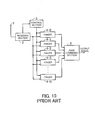
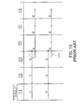
- Fig. 10 is a block diagram showing the structure of a conventional receiving unit including a Rake combining section.
- a conventional receiving unit including a Rake combining section comprises an antenna 1, a receiving section 2, a control section 3, fingers 4-0 through 4-N, and a RAKE combining section 5.
- the antenna 1 acquires radio waves sent from a base station and supplies them to the receiving section 2.
- the receiving section 2 converts the radio waves acquired by the antenna 1 into electrical signals and supplies them to the fingers 4-0 through 4-N.
- the control section 3 calculates delay time for multipath signals and supplies signals indicative of the delay time to the fingers 4-0 through 4-N respectively.
- Each of the fingers 4-0 through 4-N refers to a signal indicative of delay time, adjusts the phase of a spreading code for despreading a received signal, and demodulates a multipath component by despreading with this spreading code to obtain a desired signal.
- the RAKE combining section 5 performs a time adjustment on desired signals output from the fingers 4-0 through 4-N and performs the maximal ratio combining of the signals to generate a demodulated signal.
- the antenna 1 picks up radio waves which arrive from a base station via a plurality of paths (multipaths) and supplies them to the receiving section 2.
- the receiving section 2 converts the received signal, being a radio frequency (RF) signal, into an intermediate frequency (IF) signal, generates, for example, 8-bit I and Q signals, and outputs them.
- RF radio frequency
- IF intermediate frequency
- the transmitted waves sent from the base station will arrive via the multipaths. Accordingly, as shown in Fig. 11, the received signal has a plurality of peaks.
- the control section 3 calculates delay time for multipath signals and supplies signals indicative of the delay time to the fingers 4-0 through 4-N respectively.
- Each of the fingers 4-0 through 4-N refers to the signal indicative of delay time supplied from the control section 3, delays a despreading code by predetermined time, and performs despreading by multiplying the signal supplied from the receiving section 2 and the despreading code together.
- the Rake combining section 5 performs a time adjustment on signals output from the fingers 4-0 through 4-N after the despreading and performs the maximal ratio combining of the signals to generate a demodulated signal.
- the number of fingers which need to be provided corresponds to the number of moltipaths, resulting in large-scale circuits.
- a path on which a finger is performing despreading disappears and the same finger must perform despreading on another path component.
- a path component to be newly processed has already been received, that portion of a signal will be lost.
- Embodiments of the invention may provide a receiving unit and semiconductor device which prevent the scale of circuits from increasing and which prevent a symbol from being lost.
- a receiving unit for receiving CDMA system signals having a plurality of multipath components.
- This receiving unit comprises a receiving section for receiving a CDMA system signal, a storage section for storing the signal received by the receiving section, a demodulation section for demodulating each of multipath components included in the received signal stored in the storage section with a despreading code, a control section for controlling for demodulating a plurality of the multipath components by causing the demodulation section to perform a time division multiplex process, and a Rake combining section for performing the maximal ratio combining of output from the demodulation section to generate a demodulated signal.
- a semiconductor device for processing CDMA system signals having a plurality of multipath components comprises a receiving section for receiving a CDMA system signal, a storage section for storing the signal received by the receiving section, a demodulation section for demodulating each of multipath components included in the CDMA system signal stored in the storage section with a despreading code, a control section for controlling for demodulating a plurality of the multipath components by causing the demodulation section to perform a time division multiplex process, and a Rake combining section for performing the maximal ratio combining of output from the demodulation section to generate a demodulated signal.
- Fig. 1 is a view for describing the operative principles of the present invention.
- a receiving unit according to the present invention comprises an antenna 20, a receiving section 21, a storage section 22, a demodulation section 23, a control section 24, and a RAKE combining section 25.
- the antenna 20 acquires radio waves which arrive from a base station via multipaths.
- the receiving section 21 converts a signal acquired by the antenna 20 into the corresponding electrical signal and outputs it.
- the storage section 22 stores a signal received by the receiving section 21.
- the demodulation section 23 demodulates each of multipath components included in a received signal stored in the storage section 22 with a despreading code.
- the control section 24 supervises demodulation of a plurality of the multipath components by causing the demodulation section 23 to perform a time division multiplex process.
- the Rake combining section 25 performs the maximal ratio combining of output from the demodulation section 23 to generate a demodulated signal.
- the antenna 20 acquires electromagnetic waves arriving from a base station via multipaths and supplies them to the receiving section 21.
- the receiving section 21 converts the received waves acquired by the antenna 20 into the corresponding electrical signal, converts the electrical signal into a digital signal, and outputs the digital signal.
- the storage section 22 is a ring buffer.
- the digital signal output from the receiving section 21 is stored in order at predetermined addresses in the storage section 22. After data is stored in all the areas, data will be stored again at the leading address and the same process will be repeated.
- the demodulation section 23 reads data stored in the storage section 22 under the control of the control section 24. That is to say, the control section 24 informs the demodulation section 23 of a leading address at which each multipath component is stored. As a result, the demodulation section 23 can read each multipath component by reading predetermined data from the leading address of which the control section 24 informed the demodulation section 23. In that case, the demodulation section 23 will read data at a rate N times the rate at which writing from the receiving section 21 is performed. As a result, a single demodulation section 23 will have throughput equal to that of a total of N fingers. At the time of data being read, this can be realized by, for example, using a processing clock at a frequency N times the frequency of a processing clock used at the time of data being written into the storage section 22.
- the demodulation section 23 reads a predetermined amount (one slot) of data from the address "0001" corresponding to the address value "0001" supplied from the control section 24 at a rate three times the write rate and multiplies the data and a despreading code together for demodulation.
- the demodulation section 23 reads data from the address "0012” corresponding to the address value "0012” supplied from the control section 24 at a rate three times the write rate and multiplies the data and the despreading code together for demodulation. Similarly, the demodulation section 23 reads data from the address "0058” corresponding to the address value "0058” supplied from the control section 24 at a rate three times the write rate and multiplies the data and the despreading code together for demodulation.
- the Rake combining section 25 performs a time adjustment on the data output in order by the slot from the demodulation section 23 after demodulation and performs the maximal ratio combining of the data to obtain a demodulated signal.
- the time division multiplexing of a demodulation process is performed by writing a received signal once into the storage section 22, reading it at a rate higher than the write rate, and demodulating it by the demodulation section 23. Therefore, compared with the conventional receiving unit shown in Fig. 10, the scale of circuits can be reduced.
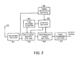
- Fig. 2 is a view showing the structure of an embodiment of the present invention.
- a receiving unit according to an embodiment of the present invention comprises an antenna 50, a receiving section 51, an input data buffer section 52, a free running counter 53, a despreading finger section 54, a control section 55, a timing detection section 56, and a RAKE combining section 57.
- the antenna 50 acquires radio waves which arrive from a base station via multipaths and supplies them to the receiving section 51.
- the receiving section 51 receives a signal acquired by the antenna 50, converts the signal into the corresponding electrical signal, and outputs it.
- a plurality of RAMs form a ring buffer.
- the input data buffer section 52 stores data supplied from the receiving section 51 at an address specified by a count value supplied from the free running counter 53.
- the free running counter 53 counts up a counter in a frame cycle and supplies a count value to the input data buffer section 52 and control section 55.
- the despreading finger section 54 reads data by the slot from addresses in the input data buffer section 52 the head of which is specified by the control section 55, and multiplies the data and a despreading code together to demodulate a received signal.
- the control section 55 controls over writing data to and reading data from the input data buffer section 52 and over the reading and despreading of data by the despreading finger section 54.
- the timing detection section 56 refers to a received signal output from the receiving section 51, detects delay time for each multipath component, generates a timing signal, and supplies it to the control section 55.
- the Rake combining section 57 performs the maximal ratio combining of output from the despreading finger section 54 to generate a demodulated signal.
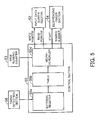
- Fig. 3 is a view showing the detailed structure of the input data buffer section 52 shown in Fig. 2.
- the input data buffer section 52 includes a decoder 52a, selectors 52b through 52d, random access memories (RAMs) 52e through 52g, and a selector 52h.
- RAMs random access memories
- the decoder 52a generates a write enable signal and write address from a write pointer supplied from the control section 55 by a decoding process and supplies them to the selectors 52b through 52d, selector 52h, and RAMs (memory areas) 52e through 52g.
- the selector 52b selects an address signal supplied from the decoder 52a and supplies it to the RAM 52e. If a write enable signal supplied from the decoder 52a is not active, then the selector 52b selects a read pointer supplied from the control section 55 and supplies it to the RAM 52e.
- a write enable signal supplied from the decoder 52a is active, then the selector 52c selects an address signal supplied from the decoder 52a and supplies it to the RAM 52f. If a write enable signal supplied from the decoder 52a is not active, then the selector 52c selects a read pointer supplied from the control section 55 and supplies a read address to the RAM 52f. If a write enable signal supplied from the decoder 52a is active, then the selector 52d selects an address signal supplied from the decoder 52a and supplies it to the RAM 52g. If a write enable signal supplied from the decoder 52a is not active, then the selector 52d selects a read pointer supplied from the control section 55 and supplies a read address to the RAM 52g.
- a write enable signal is a signal for selecting only one RAM in which data is written, so one of write enable signals supplied to the RAMs 52e through 52g is active and the others are inactive.
- the RAM 52e stores received data supplied from the receiving section 51 in a storage area corresponding to an address signal supplied from the selector 52b. If a write enable signal supplied from the decoder 52a is inactive, then the RAM 52e reads data from a storage area corresponding to an address signal supplied from the selector 52b and supplies it to the selector 52h.
- the RAM 52f stores received data supplied from the receiving section 51 in a storage area corresponding to an address signal supplied from the selector 52c. If a write enable signal supplied from the decoder 52a is inactive, then the RAM 52f reads data from a storage area corresponding to an address signal supplied from the selector 52c and supplies it to the selector 52h.
- the RAM 52g stores received data supplied from the receiving section 51 in a storage area corresponding to an address signal supplied from the selector 52d. If a write enable signal supplied from the decoder 52a is inactive, then the RAM 52g reads data from a storage area corresponding to an address signal supplied from the selector 52d and supplies it to the selector 52h.
- the selector 52h selects a RAM where data will be read out of RAMs where a write enable signal supplied from the decoder 52a is inactive, and outputs data output from the RAM to the despreading finger section 54.
- Fig. 4 is a view showing the detailed structure of the despreading finger section 54 shown in Fig. 2.
- the despreading finger section 54 includes a code generation section 54a, a multiplier 54b, an adder 54c, and a flip-flop (FF) circuit 54d.
- FF flip-flop
- the code generation section 54a generates a despreading code (obtained by adding a scrambling code and a channelization code together) corresponding to a symbol number supplied from the control section 55 in synchronization with a start signal supplied from the control section 55 and supplies it to the multiplier 54b.
- the multiplier 54b sequentially multiplies a despreading code supplied from the code generation section 54a and received data read from the input data buffer section 52 together and outputs the result.
- the adder 54c adds together the previous data stored in the FF circuit 54d and data output from the multiplier 54b and supplies the result to the FF circuit 54d.
- the FF circuit 54d stores data supplied from the adder 54c.
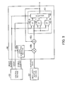
- control section 55 will be described with reference to Fig. 5.
- control section 55 includes an external register 55a, a table 55b, and a microscheduler 55c.
- the timing detection section 56 writes timing information regarding each multipath component into the external register 55a.
- the table 55b functions as a buffer.
- the table 55b reads and stores timing information written into the external register 55a in a way that will not interfere with the write operation of the external register 55a.
- the microscheduler 55c refers to a count value supplied from the free running counter 53 and generates a write pointer. Moreover, the microscheduler 55c generates a read pointer from a count value supplied from the free running counter 53 and timing information stored in the table 55b and supplies the read pointer to the input data buffer section 52.
- the microscheduler 55c refers to a count value supplied from the free running counter 53, generates a start signal periodically, and supplies it to the despreading finger section 54.
- the microscheduler 55c generates a symbol number corresponding to each multipath component and supplies it to the despreading finger section 54.
- despreading processes are performed by dividing each despread slot into sixteen despread trace slots and by assigning two despread trace slots to one finger. That is to say, each finger operates on a time division basis and eight fingers practically operate.
- the frequency of a processing clock for the despreading processes is set to a value sixteen times the frequency used in conventional receiving units.
- the total of the despread trace slots is sixteen, so there are eight too many to the eight fingers. As shown in Fig. 7, these surplus despread trace slots will be assigned to the process of preventing a symbol from being lost.
- the receiving section 51 converts the radio waves acquired by the antenna 50 into the corresponding electrical signal, converts the electrical signal into an intermediate frequency signal, converts the intermediate frequency signal into a digital signal, and supplies the digital signal to the input data buffer section 52 and timing detection section 56 as a received base band signal.
- the receiving section 51 performs fourfold oversampling on the received signal, so the receiving section 51 will output four times the amount of data it outputs in ordinary cases to the input data buffer section 52.
- the input data buffer section 52 stores the data supplied from the receiving section 51 in the RAMs 52e through 52g shown in Fig. 3 in that order.
- the input data buffer section 52 stores data in the RAM 52e again and repeats the operation of storing data in the same way. That is to say, the RAMs 52e through 52g will function as a ring buffer.
- a write pointer is supplied first from the control section 55.
- This write pointer includes a write enable (WE) signal for selecting a RAM where data is written.
- WE write enable
- This write enable signal is extracted by the decoder 52a and is supplied to the selectors 52b through 52d. If data is written into the RAM 52e, for example, a write enable signal connected to the RAM 52e out of write enable signals output from the decoder 52a becomes active and the other write enable signals become inactive.
- the write enable signal When the write enable signal becomes active, data can be written into the RAM 52e. In this case, the write enable signal is also supplied to the selector 52b. When the write enable signal becomes active, the selector 52b selects an address signal output from the decoder 52a. As a result, the address signal output from the decoder 52a will be supplied to the RAM 52e.
- the RAM 52e stores the data supplied from the receiving section 51 in a storage area specified by the address signal supplied from the selector 52b. This operation is repeated from the first address to the last address in the RAM 52e, so the RAM 52e will be filled with the data supplied from the receiving section 51.
- the receiving section 51 performs fourfold oversampling on the received signal and one chip is represented by one word (a despread slot consists of 256 chips). Therefore, a signal composing a despread slot is stored in the RAM 52e as 1024 words of data.
- the RAM 52f If the RAM 52f becomes full, then the RAM 52g will be selected as one where data can be written and data will be written into the RAM 52g. At this time data previously received is stored in the RAMs 52e and 52f. The RAM 52e or 52f therefore will be selected as one where data can be read. Data is read with a read pointer supplied from the control section 55 as a leading address and is supplied to the despreading finger section 54.
- the timing detection section 56 generates timing information regarding each multipath component, supplies the timing information to the external register 55a, and causes the external register 55a to store the timing information.
- the timing information regarding each multipath component stored in the external register 55a is stored once in the table 55b and then is read by the microscheduler 55c.
- the microscheduler 55c adds together the timing information and a count value output from the free running counter 53 to generate a read pointer.
- the read pointer generated in this way is supplied to the input data buffer section 52.
- a write enable signal connected to the RAM 52g is active and the other write enable signals are inactive.
- the selector 52d therefore selects a write address signal supplied from the decoder 52a and supplies it to the RAM 52g.
- the selector 52b selects a read pointer supplied from the control section 55 and supplies a read address to the RAM 52e.
- the selector 52c selects a read pointer supplied from the control section 55 and supplies a read address to the RAM 52f.
- Both write enable signals connected to the RAMs 52e and 52f are inactive, so data can be read from the RAMs 52e and 52f.
- the RAMs 52e and 52f read data from a storage area corresponding to a read pointer supplied from the control section 55 and supplies the data to the selector 52h.
- the selector 52h generates a signal for selecting a RAM where data is read from a write enable signal supplied from the decoder 52a, selects data output from one of the RAMs 52e through 52g on the basis of the signal, and supplies the data to the despreading finger section 54.
- the write enable signal connected to the RAM 52g is active, so the selector 52h generates a signal for selecting data output from the RAM 52e, selects data output from the RAM 52e on the basis of this signal, and outputs the data to the despreading finger section 54.
- data is also output from the RAM 52f, but this data is not selected. As a result, the data output from the RAM 52f will be discarded.
- Fig. 8 is a view for describing how data is read from the input data buffer section 52.
- RAM #M corresponds to one the RAMs 52e through 52g shown in Fig. 3 and data will be read from the RAM #M and RAM #M+1 in that order.
- M is smaller than or equal to three.
- Fig. 8 data obtained by fourfold oversampling has been written into the RAMs 52e through 52g, that is to say, the RAMs 52e through 52g store four times the amount of data used on the read side. Therefore, in the case of reading, every fourth piece of data as shown by "o" in Fig. 8 is read to reduce the amount of the data.
- positions where data is read in the case of read start addresses being 0 through 1023 are indicated. To be specific, if a read start address is, for example, 0, then data will be read from the addresses 0, 4,..., 1016, and 1020 in that order.
- a despread slot is divided into sixteen despread trace slots and is processed. Therefore, data will be read from the RAMs 52e through 52g at a rate sixteen times the ordinary (conventional) rate. For example, the frequency of a processing clock at the time of data being read is sixteen times higher than that of a processing clock (ordinary processing clock) at the time of data being written.
- An ordinary despreading process will be performed on despread trace slots bearing even numbers (TR#0, TR#2, TR#4,..., and TR#14) included in data read in this way.
- a despreading process will be performed on despread trace slots bearing odd numbers (TR#1, TR#3, TR#5,..., and TR#15) only to make compensation for preventing a symbol from being lost.
- the despreading finger section 54 accepts data read by the input data buffer section 52 and supplies it to the multiplier 54b.
- the code generation section 54a supplies a despreading code, which is obtained by adding a scrambling code and a channelization code together, corresponding to a symbol number supplied from the control section 55.
- the multiplier 54b sequentially multiplies the data read by the input data buffer section 52 and the despreading code supplied from the code generation section 54a together and outputs the result.
- the adder 54c adds together the data output from the multiplier 54b and a value, which was obtained by the previous operation and which is stored in the FF 54d, and outputs the result.
- the FF 54d stores the operation result output from the adder 54c.
- the output from the FF 54d will be values obtained by integrating results obtained by multiplying the data read by the input data buffer section 52 and the despreading code supplied from the code generation section 54a together.
- the values obtained in this way by the integration are supplied to the Rake combining section 57.
- the Rake combining section 57 performs the maximal ratio combining of the values to generate a demodulated signal.
- the input data buffer section 52 is located between the receiving section 51 and the despreading finger section 54 and a time division multiplex process is performed in the despreading finger section 54 by setting a data read rate higher than a data write rate. This enables one despreading finger section 54 to play a role equal to a plurality of despreading finger sections. As a result, the scale of circuits can be reduced.
- surplus despread trace slots are provided in the case of reading data from the input data buffer section 52 and a compensation process is performed in these surplus slots if necessary. This prevents a symbol from being lost.
- a despread slot is divided into sixteen despread trace slots.
- the present invention is not limited to such a case.
- Fig. 9 is a view showing another example of the structure of the despreading finger section 54 shown in Fig. 2.
- a despreading finger section 60 shown in Fig. 9 comprises a code generation section 60a, a multiplier 60b, an adder 60c, and a buffer section 61 including FF circuits 62-0 through 62-N and a selector 63.
- the code generation section 60a When a start signal supplied from the control section 55 becomes active, the code generation section 60a generates a despreading code corresponding to a symbol number, which is obtained by adding a scrambling code and a channelization code together, and supplies it to the multiplier 60b.
- the multiplier 60b sequentially multiplies data read by the input data buffer section 52 and a despreading code supplied from the code generation section 60a together and outputs the result.
- the adder 60c adds together data output from the multiplier 60b and data stored in the buffer section 61 and supplies the result to the buffer section 61.
- the input data buffer section 52 reads data the amount of which is half of a slot shown in Fig. 6(B), that is to say, 128 chips of data and outputs it.
- the selector 63 refers to a finger number supplied from the control section 55 and selects output from the FF circuit 62-0. Therefore, the 128 chips of data corresponding to the first finger and a despreading code are multiplied together and the obtained values are integrated. The result of the integration is stored in the FF circuit 62-0.
- the selector 63 selects output from the FF circuit 62-1 and performs the same process as described above. Therefore, 128 chips of data corresponding to a second finger and the despreading code are multiplied together and the obtained values are integrated. The result of the integration is stored in the FF circuit 62-1.
- data corresponding to the second half of a despread slot is read by the 128 chips and a despreading process is performed on this data in the same way as described above.
- the selector 63 in the despreading finger section 60 selects output from the FF circuit 62-0.
- the FF circuit 62-0 stores the result of the operation in which 128 chips of data corresponding to the first half of a despread slot was used, so the result of an operation in which the 128 chips of data corresponding to the second half of a despread slot is used will be added. As a result, the result of a despreading process on all the 256 chips of data composing a despread slot will be obtained.
- the selector 63 selects output from the FF circuit 62-1 and performs the same process as described above. As a result, the result of a despreading process on data corresponding to the second finger will be obtained.
- data is read from the input data buffer section 52 by the 128 chips. Therefore, the storage capacity of the RAMs 52e through 52g included in the input data buffer section 52 can be reduced by half.
- a receiving unit for receiving CDMA system signals having a plurality of multipath components comprises a receiving section for receiving a CDMA system signal, a storage section for storing the signal received by the receiving section, a demodulation section for demodulating each of multipath components included in the received signal stored in the storage section with a despreading code, a control section for controlling demodulation of a plurality of the multipath components by causing the demodulation section to perform a time division multiplex process, and a Rake combining section for performing the maximal ratio combining of output from the demodulation section to generate a demodulated signal. This prevents a symbol from being lost.
- a semiconductor device for processing CDMA system signals having a plurality of multipath components comprises a receiving section for receiving a CDMA system signal, a storage section for storing the signal received by the receiving section, a demodulation section for demodulating each of multipath components included in the CDMA system signal stored in the storage section with a despreading code, a control section for controlling for demodulating a plurality of the multipath components by causing the demodulation section to perform a time division multiplex process, and a Rake combining section for performing the maximal ratio combining of output from the demodulation section to generate a demodulated signal.
- This can reduce the size of semiconductor devices.
Landscapes
- Engineering & Computer Science (AREA)
- Computer Networks & Wireless Communication (AREA)
- Signal Processing (AREA)
- Mobile Radio Communication Systems (AREA)
- Noise Elimination (AREA)
Applications Claiming Priority (2)
| Application Number | Priority Date | Filing Date | Title |
|---|---|---|---|
| JP2001310345 | 2001-10-05 | ||
| JP2001310345A JP3871540B2 (ja) | 2001-10-05 | 2001-10-05 | 受信装置および半導体装置 |
Publications (3)
| Publication Number | Publication Date |
|---|---|
| EP1300961A2 true EP1300961A2 (fr) | 2003-04-09 |
| EP1300961A3 EP1300961A3 (fr) | 2004-12-01 |
| EP1300961B1 EP1300961B1 (fr) | 2014-08-13 |
Family
ID=19129334
Family Applications (1)
| Application Number | Title | Priority Date | Filing Date |
|---|---|---|---|
| EP20020251992 Expired - Lifetime EP1300961B1 (fr) | 2001-10-05 | 2002-03-20 | Unité de réception et dispositif semi-conducteur |
Country Status (4)
| Country | Link |
|---|---|
| US (1) | US7035318B2 (fr) |
| EP (1) | EP1300961B1 (fr) |
| JP (1) | JP3871540B2 (fr) |
| CN (1) | CN1208919C (fr) |
Cited By (2)
| Publication number | Priority date | Publication date | Assignee | Title |
|---|---|---|---|---|
| EP1976138A3 (fr) * | 2007-03-30 | 2009-05-20 | MediaTek, Inc | Doigts de rake partagés et dispositif de recherche de trajets |
| US20090285266A1 (en) * | 2008-05-13 | 2009-11-19 | Fujitsu Limited | Rake receiving device, base station apparatus, reception control method, and reception control program |
Families Citing this family (7)
| Publication number | Priority date | Publication date | Assignee | Title |
|---|---|---|---|---|
| US6771693B2 (en) | 2001-12-27 | 2004-08-03 | Interdigital Technology Corporation | Enhanced rake structure |
| US7103091B2 (en) * | 2002-05-07 | 2006-09-05 | Stmicroelectronics, Inc. | Common data path rake receiver for a CDMA demodulator circuit |
| US7596134B2 (en) * | 2002-07-03 | 2009-09-29 | Freescale Semiconductor, Inc. | Flexible method and apparatus for performing digital modulation and demodulation |
| CN101371464A (zh) * | 2005-12-14 | 2009-02-18 | 艾利森电话股份有限公司 | 用于扩频接收器的按要求解扩 |
| CN101127973B (zh) * | 2006-12-18 | 2011-11-02 | 浙江华立通信集团有限公司 | Td-scdma/3g/4g终端多径接收合并器 |
| CN103546193B (zh) * | 2012-07-09 | 2017-02-08 | 中兴通讯股份有限公司 | 重构处理方法及装置 |
| WO2025197303A1 (fr) * | 2024-03-21 | 2025-09-25 | ソニーセミコンダクタソリューションズ株式会社 | Dispositif de calcul de produit-somme et circuit intégré |
Citations (1)
| Publication number | Priority date | Publication date | Assignee | Title |
|---|---|---|---|---|
| EP0998052A2 (fr) | 1998-10-30 | 2000-05-03 | Hitachi, Ltd. | Appareil de communication |
Family Cites Families (7)
| Publication number | Priority date | Publication date | Assignee | Title |
|---|---|---|---|---|
| US5682403A (en) * | 1995-05-04 | 1997-10-28 | Wavelink Communications | Spread spectrum communication network signal processor |
| FR2737362B1 (fr) * | 1995-07-25 | 1997-10-10 | Matra Communication | Procede de selection des retards de propagation retenus pour recevoir des messages transmis par radiocommunication a etalement de spectre |
| JP2820918B2 (ja) * | 1996-03-08 | 1998-11-05 | 株式会社ワイ・アール・ピー移動通信基盤技術研究所 | スペクトル拡散通信装置 |
| US5903550A (en) * | 1997-01-02 | 1999-05-11 | Motorola, Inc. | Method and system for parallel demodulation of multiple chips of a CDMA signal |
| EP1107471B1 (fr) * | 1999-12-10 | 2006-03-08 | Lucent Technologies Inc. | Doigt de récepteur RAKE à multiplexage temporal pour WCDMA |
| JP3414353B2 (ja) * | 2000-03-15 | 2003-06-09 | 日本電気株式会社 | Cdma復調装置及びその方法 |
| ES2420487T3 (es) * | 2000-07-31 | 2013-08-23 | Intel Mobile Communications GmbH | Aparato y métodos para selección por muestreo y reutilización de dedos de rastrillo en sistemas de espectro ensanchado o difundido |
-
2001
- 2001-10-05 JP JP2001310345A patent/JP3871540B2/ja not_active Expired - Fee Related
-
2002
- 2002-03-20 EP EP20020251992 patent/EP1300961B1/fr not_active Expired - Lifetime
- 2002-03-26 US US10/105,191 patent/US7035318B2/en not_active Expired - Lifetime
- 2002-04-12 CN CNB021059683A patent/CN1208919C/zh not_active Expired - Fee Related
Patent Citations (1)
| Publication number | Priority date | Publication date | Assignee | Title |
|---|---|---|---|---|
| EP0998052A2 (fr) | 1998-10-30 | 2000-05-03 | Hitachi, Ltd. | Appareil de communication |
Cited By (4)
| Publication number | Priority date | Publication date | Assignee | Title |
|---|---|---|---|---|
| EP1976138A3 (fr) * | 2007-03-30 | 2009-05-20 | MediaTek, Inc | Doigts de rake partagés et dispositif de recherche de trajets |
| US8125973B2 (en) | 2007-03-30 | 2012-02-28 | Mediatek Inc. | Time shared rake fingers and path searcher |
| US20090285266A1 (en) * | 2008-05-13 | 2009-11-19 | Fujitsu Limited | Rake receiving device, base station apparatus, reception control method, and reception control program |
| EP2120355A3 (fr) * | 2008-05-13 | 2010-01-13 | Fujitsu Limited | Dispositif de réception rake, appareil de station de base, procédé de contrôle de réception, et programme de contrôle de réception |
Also Published As
| Publication number | Publication date |
|---|---|
| JP2003115821A (ja) | 2003-04-18 |
| EP1300961B1 (fr) | 2014-08-13 |
| US20030067965A1 (en) | 2003-04-10 |
| CN1208919C (zh) | 2005-06-29 |
| JP3871540B2 (ja) | 2007-01-24 |
| CN1411193A (zh) | 2003-04-16 |
| US7035318B2 (en) | 2006-04-25 |
| EP1300961A3 (fr) | 2004-12-01 |
Similar Documents
| Publication | Publication Date | Title |
|---|---|---|
| JP4283216B2 (ja) | Cdma通信システムにおける柔軟な相関と待ち行列 | |
| US7065128B2 (en) | Apparatus and methods for sample selection and reuse of rake fingers in spread spectrum systems | |
| KR100606223B1 (ko) | 개량형 레이크 구조체 | |
| EP1300961B1 (fr) | Unité de réception et dispositif semi-conducteur | |
| US6480527B1 (en) | CDMA demodulating method and demodulator | |
| US7236516B2 (en) | RAKE receiver device | |
| JP2001223611A (ja) | 受信装置 | |
| KR100380770B1 (ko) | 확산 스펙트럼 수신기 | |
| EP1908177B1 (fr) | Correlateur pour recherche de piles au moyen d'une architecture memoire | |
| JP2004072418A (ja) | 遅延プロファイル作成方法および遅延プロファイル作成装置 | |
| JP2002305466A (ja) | レイク受信装置 | |
| JPH1174820A (ja) | Cdma信号受信装置 | |
| US6834074B2 (en) | Method of time tracking in a vector correlator based rake receiver | |
| JP2002164812A (ja) | スペクトラム拡散通信用パスサーチ回路 | |
| US7689739B2 (en) | Spread spectrum receiver, apparatus and method of a circular buffer for multirate data | |
| US7706427B2 (en) | Method and apparatus for compact OVSF despreading | |
| KR100228012B1 (ko) | 메모리를 이용한 심볼 결합 장치 및 그 방법 | |
| EP1463212A1 (fr) | Récepteur AMRC, procédé et programme de gestion de voie | |
| JP2000278180A (ja) | Cdma受信機 | |
| KR20030054303A (ko) | 부호 분할 다중 접속 시스템용 기지국 복조기에서의 칩연산 장치 및 그 방법과, 그 장치를 사용한 기지국 복조기 | |
| KR20050078064A (ko) | 기지국 수신기에서의 다중 경로 신호 컴바이닝을 위한시간 조정 버퍼 제어 장치 및 제어방법 | |
| JP2005176006A (ja) | Cdma通信システム用逆拡散多重回路 | |
| JP2003078450A (ja) | 相関検出器 |
Legal Events
| Date | Code | Title | Description |
|---|---|---|---|
| PUAI | Public reference made under article 153(3) epc to a published international application that has entered the european phase |
Free format text: ORIGINAL CODE: 0009012 |
|
| AK | Designated contracting states |
Kind code of ref document: A2 Designated state(s): AT BE CH CY DE DK ES FI FR GB GR IE IT LI LU MC NL PT SE TR |
|
| AX | Request for extension of the european patent |
Extension state: AL LT LV MK RO SI |
|
| PUAL | Search report despatched |
Free format text: ORIGINAL CODE: 0009013 |
|
| AK | Designated contracting states |
Kind code of ref document: A3 Designated state(s): AT BE CH CY DE DK ES FI FR GB GR IE IT LI LU MC NL PT SE TR |
|
| AX | Request for extension of the european patent |
Extension state: AL LT LV MK RO SI |
|
| 17P | Request for examination filed |
Effective date: 20050527 |
|
| AKX | Designation fees paid |
Designated state(s): DE FR GB |
|
| RAP1 | Party data changed (applicant data changed or rights of an application transferred) |
Owner name: FUJITSU MICROELECTRONICS LIMITED |
|
| 17Q | First examination report despatched |
Effective date: 20100115 |
|
| RAP1 | Party data changed (applicant data changed or rights of an application transferred) |
Owner name: FUJITSU SEMICONDUCTOR LIMITED |
|
| GRAP | Despatch of communication of intention to grant a patent |
Free format text: ORIGINAL CODE: EPIDOSNIGR1 |
|
| INTG | Intention to grant announced |
Effective date: 20140307 |
|
| RIN1 | Information on inventor provided before grant (corrected) |
Inventor name: KANASUGI, MASAMI Inventor name: YAMADA, YOSHIKAZU Inventor name: KUROIWA, KOICHI Inventor name: HIKITA, MAHIRO Inventor name: TANIGUCHI, SHOJI |
|
| GRAS | Grant fee paid |
Free format text: ORIGINAL CODE: EPIDOSNIGR3 |
|
| GRAA | (expected) grant |
Free format text: ORIGINAL CODE: 0009210 |
|
| AK | Designated contracting states |
Kind code of ref document: B1 Designated state(s): DE FR GB |
|
| REG | Reference to a national code |
Ref country code: GB Ref legal event code: FG4D |
|
| REG | Reference to a national code |
Ref country code: DE Ref legal event code: R096 Ref document number: 60246520 Country of ref document: DE Effective date: 20140918 |
|
| REG | Reference to a national code |
Ref country code: DE Ref legal event code: R082 Ref document number: 60246520 Country of ref document: DE Representative=s name: HOFFMANN - EITLE PATENT- UND RECHTSANWAELTE PA, DE |
|
| REG | Reference to a national code |
Ref country code: DE Ref legal event code: R097 Ref document number: 60246520 Country of ref document: DE |
|
| REG | Reference to a national code |
Ref country code: DE Ref legal event code: R081 Ref document number: 60246520 Country of ref document: DE Owner name: SOCIONEXT INC., YOKOHAMA-SHI, JP Free format text: FORMER OWNER: FUJITSU LTD., KANAGAWA, JP Effective date: 20140813 Ref country code: DE Ref legal event code: R081 Ref document number: 60246520 Country of ref document: DE Owner name: SOCIONEXT INC., YOKOHAMA-SHI, JP Free format text: FORMER OWNER: FUJITSU SEMICONDUCTOR LTD., YOKOHAMA-SHI, KANAGAWA, JP Effective date: 20150512 Ref country code: DE Ref legal event code: R082 Ref document number: 60246520 Country of ref document: DE Representative=s name: HOFFMANN - EITLE PATENT- UND RECHTSANWAELTE PA, DE Effective date: 20150512 |
|
| PLBE | No opposition filed within time limit |
Free format text: ORIGINAL CODE: 0009261 |
|
| STAA | Information on the status of an ep patent application or granted ep patent |
Free format text: STATUS: NO OPPOSITION FILED WITHIN TIME LIMIT |
|
| 26N | No opposition filed |
Effective date: 20150515 |
|
| GBPC | Gb: european patent ceased through non-payment of renewal fee |
Effective date: 20150320 |
|
| REG | Reference to a national code |
Ref country code: FR Ref legal event code: ST Effective date: 20151130 |
|
| PG25 | Lapsed in a contracting state [announced via postgrant information from national office to epo] |
Ref country code: GB Free format text: LAPSE BECAUSE OF NON-PAYMENT OF DUE FEES Effective date: 20150320 |
|
| PG25 | Lapsed in a contracting state [announced via postgrant information from national office to epo] |
Ref country code: FR Free format text: LAPSE BECAUSE OF NON-PAYMENT OF DUE FEES Effective date: 20150331 |
|
| PGFP | Annual fee paid to national office [announced via postgrant information from national office to epo] |
Ref country code: DE Payment date: 20180306 Year of fee payment: 17 |
|
| REG | Reference to a national code |
Ref country code: DE Ref legal event code: R119 Ref document number: 60246520 Country of ref document: DE |
|
| PG25 | Lapsed in a contracting state [announced via postgrant information from national office to epo] |
Ref country code: DE Free format text: LAPSE BECAUSE OF NON-PAYMENT OF DUE FEES Effective date: 20191001 |