EP1301432B1 - Procede de fabrication de dispositifs renfermant des systemes micromecaniques utilisant des bandes a durcissement par ultraviolet - Google Patents
Procede de fabrication de dispositifs renfermant des systemes micromecaniques utilisant des bandes a durcissement par ultraviolet Download PDFInfo
- Publication number
- EP1301432B1 EP1301432B1 EP01927493A EP01927493A EP1301432B1 EP 1301432 B1 EP1301432 B1 EP 1301432B1 EP 01927493 A EP01927493 A EP 01927493A EP 01927493 A EP01927493 A EP 01927493A EP 1301432 B1 EP1301432 B1 EP 1301432B1
- Authority
- EP
- European Patent Office
- Prior art keywords
- substrate
- mems
- holding means
- wafer
- light
- Prior art date
- Legal status (The legal status is an assumption and is not a legal conclusion. Google has not performed a legal analysis and makes no representation as to the accuracy of the status listed.)
- Expired - Lifetime
Links
Images




Classifications
-
- B—PERFORMING OPERATIONS; TRANSPORTING
- B81—MICROSTRUCTURAL TECHNOLOGY
- B81C—PROCESSES OR APPARATUS SPECIALLY ADAPTED FOR THE MANUFACTURE OR TREATMENT OF MICROSTRUCTURAL DEVICES OR SYSTEMS
- B81C1/00—Manufacture or treatment of devices or systems in or on a substrate
- B81C1/00865—Multistep processes for the separation of wafers into individual elements
- B81C1/00904—Multistep processes for the separation of wafers into individual elements not provided for in groups B81C1/00873 - B81C1/00896
-
- H—ELECTRICITY
- H10—SEMICONDUCTOR DEVICES; ELECTRIC SOLID-STATE DEVICES NOT OTHERWISE PROVIDED FOR
- H10P—GENERIC PROCESSES OR APPARATUS FOR THE MANUFACTURE OR TREATMENT OF DEVICES COVERED BY CLASS H10
- H10P72/00—Handling or holding of wafers, substrates or devices during manufacture or treatment thereof
- H10P72/70—Handling or holding of wafers, substrates or devices during manufacture or treatment thereof for supporting or gripping
- H10P72/74—Handling or holding of wafers, substrates or devices during manufacture or treatment thereof for supporting or gripping using temporarily an auxiliary support
-
- H—ELECTRICITY
- H10—SEMICONDUCTOR DEVICES; ELECTRIC SOLID-STATE DEVICES NOT OTHERWISE PROVIDED FOR
- H10P—GENERIC PROCESSES OR APPARATUS FOR THE MANUFACTURE OR TREATMENT OF DEVICES COVERED BY CLASS H10
- H10P72/00—Handling or holding of wafers, substrates or devices during manufacture or treatment thereof
- H10P72/70—Handling or holding of wafers, substrates or devices during manufacture or treatment thereof for supporting or gripping
- H10P72/74—Handling or holding of wafers, substrates or devices during manufacture or treatment thereof for supporting or gripping using temporarily an auxiliary support
- H10P72/7402—Wafer tapes, e.g. grinding or dicing support tapes
-
- H—ELECTRICITY
- H10—SEMICONDUCTOR DEVICES; ELECTRIC SOLID-STATE DEVICES NOT OTHERWISE PROVIDED FOR
- H10P—GENERIC PROCESSES OR APPARATUS FOR THE MANUFACTURE OR TREATMENT OF DEVICES COVERED BY CLASS H10
- H10P72/00—Handling or holding of wafers, substrates or devices during manufacture or treatment thereof
- H10P72/70—Handling or holding of wafers, substrates or devices during manufacture or treatment thereof for supporting or gripping
- H10P72/74—Handling or holding of wafers, substrates or devices during manufacture or treatment thereof for supporting or gripping using temporarily an auxiliary support
- H10P72/7412—Handling or holding of wafers, substrates or devices during manufacture or treatment thereof for supporting or gripping using temporarily an auxiliary support the auxiliary support including means facilitating the separation of a device or wafer from the auxiliary support
- H10P72/7414—Handling or holding of wafers, substrates or devices during manufacture or treatment thereof for supporting or gripping using temporarily an auxiliary support the auxiliary support including means facilitating the separation of a device or wafer from the auxiliary support the auxiliary support including means facilitating the selective separation of some of a plurality of devices from the auxiliary support
-
- H—ELECTRICITY
- H10—SEMICONDUCTOR DEVICES; ELECTRIC SOLID-STATE DEVICES NOT OTHERWISE PROVIDED FOR
- H10P—GENERIC PROCESSES OR APPARATUS FOR THE MANUFACTURE OR TREATMENT OF DEVICES COVERED BY CLASS H10
- H10P72/00—Handling or holding of wafers, substrates or devices during manufacture or treatment thereof
- H10P72/70—Handling or holding of wafers, substrates or devices during manufacture or treatment thereof for supporting or gripping
- H10P72/74—Handling or holding of wafers, substrates or devices during manufacture or treatment thereof for supporting or gripping using temporarily an auxiliary support
- H10P72/7416—Handling or holding of wafers, substrates or devices during manufacture or treatment thereof for supporting or gripping using temporarily an auxiliary support used during dicing or grinding
-
- H—ELECTRICITY
- H10—SEMICONDUCTOR DEVICES; ELECTRIC SOLID-STATE DEVICES NOT OTHERWISE PROVIDED FOR
- H10P—GENERIC PROCESSES OR APPARATUS FOR THE MANUFACTURE OR TREATMENT OF DEVICES COVERED BY CLASS H10
- H10P72/00—Handling or holding of wafers, substrates or devices during manufacture or treatment thereof
- H10P72/70—Handling or holding of wafers, substrates or devices during manufacture or treatment thereof for supporting or gripping
- H10P72/74—Handling or holding of wafers, substrates or devices during manufacture or treatment thereof for supporting or gripping using temporarily an auxiliary support
- H10P72/7422—Handling or holding of wafers, substrates or devices during manufacture or treatment thereof for supporting or gripping using temporarily an auxiliary support used to protect an active side of a device or wafer
-
- H—ELECTRICITY
- H10—SEMICONDUCTOR DEVICES; ELECTRIC SOLID-STATE DEVICES NOT OTHERWISE PROVIDED FOR
- H10P—GENERIC PROCESSES OR APPARATUS FOR THE MANUFACTURE OR TREATMENT OF DEVICES COVERED BY CLASS H10
- H10P72/00—Handling or holding of wafers, substrates or devices during manufacture or treatment thereof
- H10P72/70—Handling or holding of wafers, substrates or devices during manufacture or treatment thereof for supporting or gripping
- H10P72/74—Handling or holding of wafers, substrates or devices during manufacture or treatment thereof for supporting or gripping using temporarily an auxiliary support
- H10P72/744—Details of chemical or physical process used for separating the auxiliary support from a device or a wafer
-
- Y—GENERAL TAGGING OF NEW TECHNOLOGICAL DEVELOPMENTS; GENERAL TAGGING OF CROSS-SECTIONAL TECHNOLOGIES SPANNING OVER SEVERAL SECTIONS OF THE IPC; TECHNICAL SUBJECTS COVERED BY FORMER USPC CROSS-REFERENCE ART COLLECTIONS [XRACs] AND DIGESTS
- Y10—TECHNICAL SUBJECTS COVERED BY FORMER USPC
- Y10S—TECHNICAL SUBJECTS COVERED BY FORMER USPC CROSS-REFERENCE ART COLLECTIONS [XRACs] AND DIGESTS
- Y10S438/00—Semiconductor device manufacturing: process
- Y10S438/977—Thinning or removal of substrate
-
- Y—GENERAL TAGGING OF NEW TECHNOLOGICAL DEVELOPMENTS; GENERAL TAGGING OF CROSS-SECTIONAL TECHNOLOGIES SPANNING OVER SEVERAL SECTIONS OF THE IPC; TECHNICAL SUBJECTS COVERED BY FORMER USPC CROSS-REFERENCE ART COLLECTIONS [XRACs] AND DIGESTS
- Y10—TECHNICAL SUBJECTS COVERED BY FORMER USPC
- Y10T—TECHNICAL SUBJECTS COVERED BY FORMER US CLASSIFICATION
- Y10T156/00—Adhesive bonding and miscellaneous chemical manufacture
- Y10T156/10—Methods of surface bonding and/or assembly therefor
- Y10T156/1052—Methods of surface bonding and/or assembly therefor with cutting, punching, tearing or severing
-
- Y—GENERAL TAGGING OF NEW TECHNOLOGICAL DEVELOPMENTS; GENERAL TAGGING OF CROSS-SECTIONAL TECHNOLOGIES SPANNING OVER SEVERAL SECTIONS OF THE IPC; TECHNICAL SUBJECTS COVERED BY FORMER USPC CROSS-REFERENCE ART COLLECTIONS [XRACs] AND DIGESTS
- Y10—TECHNICAL SUBJECTS COVERED BY FORMER USPC
- Y10T—TECHNICAL SUBJECTS COVERED BY FORMER US CLASSIFICATION
- Y10T156/00—Adhesive bonding and miscellaneous chemical manufacture
- Y10T156/10—Methods of surface bonding and/or assembly therefor
- Y10T156/1052—Methods of surface bonding and/or assembly therefor with cutting, punching, tearing or severing
- Y10T156/1062—Prior to assembly
- Y10T156/1064—Partial cutting [e.g., grooving or incising]
-
- Y—GENERAL TAGGING OF NEW TECHNOLOGICAL DEVELOPMENTS; GENERAL TAGGING OF CROSS-SECTIONAL TECHNOLOGIES SPANNING OVER SEVERAL SECTIONS OF THE IPC; TECHNICAL SUBJECTS COVERED BY FORMER USPC CROSS-REFERENCE ART COLLECTIONS [XRACs] AND DIGESTS
- Y10—TECHNICAL SUBJECTS COVERED BY FORMER USPC
- Y10T—TECHNICAL SUBJECTS COVERED BY FORMER US CLASSIFICATION
- Y10T428/00—Stock material or miscellaneous articles
- Y10T428/14—Layer or component removable to expose adhesive
- Y10T428/149—Sectional layer removable
- Y10T428/1495—Adhesive is on removable layer
Definitions
- This invention relates to the fabrication of devices incorporating microelectromechanical systems (MEMS). More particularly, the invention relates to a method of fabricating MEMS devices using UV curable tapes.
- MEMS microelectromechanical systems
- a MEMS device and the part of the device comprising the microelectromechanical system shall be referred to as a MEMS layer.
- US-A-5904546 discloses an abrasiveless method and apparatus for dicing semiconductor wafers, in which a backside wet etch is used to separate the individual semiconductor chips.
- Patent Abstracts of Japan vol. 1997, no. 01, 31 Jan 1997 and JP08250454 A discloses another method of dicing a semiconductor wafer into individual chips.
- the method includes bonding the holding means to the substrate.
- a handling means may be applied to the holding means.
- the handle wafer may impart rigidity and may facilitate manipulation of a laminate, the laminate comprising the substrate and the MEMS layer.
- the operations performed on the substrate may include thinning the substrate and include etching the substrate from the opposed side of the substrate to divide the substrate into individual chips. Further, the operations performed on the MEMS layer include removing sacrificial material from the layer to release individual MEMS chips.
- the MEMS chip may comprise a part of the substrate and at least one MEMS element or component.
- the method may include applying the holding means to the substrate before removal of the handle water and the adhesive tape.
- the holding means may also be bonded to the substrate.
- Both the curable adhesive tape and the second holding means may be in the form of tapes which have adhesives which are curable by exposure to ultraviolet (UV) light
- UV ultraviolet
- the method may include exposing localised regions of the holding means to the UV light to release one MEMS chip at a time from the holding means to enable each MEMS chip to be removed individually from the holding means.
- the method may include applying a handling means to the holding means.
- the handling means may be transparent to the UV light so that the UV light is transmitted through the handling means to cure the adhesive of the holding means.
- Each handling means may be in the form of a glass, quartz, alumina or equivalent wafer.
- the method may finally include removing each chip from the holding means by a transporting means.
- a silicon substrate or wafer 12 is provided.
- the wafer 12 carries a surface micromachined MEMS layer 14 on a first surface 16 of the wafer 12.
- the MEMS layer 14 has a plurality of MEMS elements or chips 18 interposed in one or more sacrificial layers 20.
- a first holding means in the form of an adhesive tape 22, is bonded to the MEMS layer 14 as illustrated in Figure 2 of the drawings.
- the tape 22 is bonded to the layer 14 by means of a curable adhesive.
- the adhesive is curable in the sense that it loses its adhesive properties or "tackiness" when exposed to ultraviolet (UV) light.
- a handling means in the form of a glass, quartz, alumina or other transparent handle wafer 24 is secured to the tape 22.
- a laminate 26, comprising the silicon wafer 12, the MEMS layer 14, the tape 22 and the glass wafer 24 is then turned over to expose an opposed side 28 of the silicon wafer 12.
- a first operation is performed on the silicon wafer 12 by back grinding a surface 28.1 of the opposed side 28 of the silicon wafer 12 to thin the wafer 12 as illustrated in Figure 4 of the drawings. This reduces the etch time of the silicon wafer 12.
- each chip 30 has one MEMS element 18 associated with it but it will be appreciated that each chip 30 could, if desired, contain an array of MEMS elements.
- a second holding means in the form of a second tape 32 is applied to the surface 28.1 of the silicon wafer 12.
- a second transparent handle wafer 34 is applied to the tape 32, depending on the equipment being used.
- the tape 32 is bonded to the surface 28.1 of the wafer 12 by means of an adhesive which is also curable when exposed to UV light.
- the first tape 22 and the glass wafer 24 are removed, as illustrated schematically by anew 36 in Figure 7 of the drawings, after application of the tape 32.
- the tape 22 is removed by exposing it to UV light which is projected on to the tape 22 through the glass layer 24 as illustrated by arrows 38.
- the glass wafer 24 is transparent to the UV light.
- the silicon wafer 12 is opaque to the UV light so that the tape 32 on the other side of the wafer 12 is not affected by the UV light when the tape 22 is exposed to the UV light.
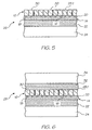
- a new laminate 40 comprising the silicon wafer 12, the MEMS layer 14, the tape 32 and the glass wafer 34 is turned over to expose the sacrificial layer 20 of the MEMS layer 14.
- the sacrificial layer 20 is then removed by etching or by oxygen plasma techniques. This releases the MEMS elements 18, and completes the separation of the chips 42.
- the laminate 40 is placed on an xy wafer stage (not shown) which is reciprocated, as illustrated by arrow 44 in Figure 10 of the drawings.
- Each MEMS chip 42 when it is desired to remove it, is exposed to UV light as indicated by arrows 46 through a mask 50. This cures the adhesive of the tape 32 locally beneath one particular MEMS chip 42 at a time, to enable that MEMS chip 42 to be removed from the tape 32 by means of a transporting means which may include a vacuum pickup 48.
- the MEMS elements 18 comprise nozzle assemblies. Each assembly comprises an ink ejection nozzle and an actuator for controlling ink ejection.
- the manufacturing process facilitates that the MEMS devices 18 are not touched by solids or liquids after they are released by the release etch.
Landscapes
- Engineering & Computer Science (AREA)
- Manufacturing & Machinery (AREA)
- Microelectronics & Electronic Packaging (AREA)
- Micromachines (AREA)
- Dicing (AREA)
Abstract
Claims (7)
- - Procédé de fabrication de dispositifs MEMS (Micro Electro Mechanical Systems - Microsystèmes Electromécaniques), le procédé comprenant les étapes consistant à :- prendre un substrat (12) avec une couche de MEMS (14) disposée sur un côté du substrat, ladite couche de MEMS comprenant une pluralité d'éléments de MEMS (18) interposés dans une ou plusieurs couches sacrificielles (20) :- lier une plaquette de manipulation (24) à la couche de MEMS (14) à l'aide d'une bande adhésive durcissable (22) ;- effectuer au moins une opération sur le substrat à partir d'un côté du substrat opposé au côté ayant la couche de MEMS (14), ladite ou lesdites opérations comprenant une gravure de silicium profonde à travers la plaquette pour couper la plaquette en puces et former des puces individuelles ;- appliquer un moyen de support (32) sur ledit côté opposé du substrat ;- retirer la plaquette de manipulation (24) et la bande adhésive (22) ;- effectuer au moins une opération sur la couche de MEMS (14) pour libérer lesdits éléments de MEMS (18) et achever la séparation des puces par retrait de ladite couche sacrificielle ; et- amener les puces individuelles (42) à être libérées du moyen de support (32) pour le retrait du moyen de support.
- - Procédé selon la revendication 1, dans lequel ladite ou lesdites opérations effectuées sur le substrat comprennent en outre l'amincissement du substrat (12).
- - Procédé selon la revendication 1, qui comprend l'application du moyen de support (32) sur le substrat avant le retrait de la plaquette de manipulation (24) et de la bande adhésive (22).
- - Procédé selon la revendication 1, qui comprend la liaison du moyen de support (24) au substrat (12).
- - Procédé selon la revendication 4, dans lequel le moyen de support (24) est lié au substrat (12) au moyen d'un adhésif qui est durcissable par exposition à la lumière ultraviolette (UV), et dans lequel le procédé comprend l'exposition de régions localisées du moyen de support (32) à la lumière UV pour libérer une puce à la fois à partir du moyen de support (32) pour permettre à chaque puce d'être retirée individuellement du moyen de support (32).
- - Procédé selon la revendication 5, qui comprend l'application d'un moyen de manipulation (34) sur le moyen de support (32), le moyen de manipulation étant transparent à la lumière UV de telle sorte que la lumière UV est transmise à travers le moyen de manipulation pour faire durcir l'adhésif du moyen de support.
- - Procédé selon la revendication 6, qui comprend le retrait de chaque puce (42) du moyen de support par un moyen de transport (48).
Applications Claiming Priority (3)
| Application Number | Priority Date | Filing Date | Title |
|---|---|---|---|
| US567951 | 2000-05-10 | ||
| US09/567,951 US6425971B1 (en) | 2000-05-10 | 2000-05-10 | Method of fabricating devices incorporating microelectromechanical systems using UV curable tapes |
| PCT/AU2001/000502 WO2001085600A1 (fr) | 2000-05-10 | 2001-05-02 | Procede de fabrication de dispositifs renfermant des systemes micromecaniques utilisant des bandes a durcissement par ultraviolet |
Publications (3)
| Publication Number | Publication Date |
|---|---|
| EP1301432A1 EP1301432A1 (fr) | 2003-04-16 |
| EP1301432A4 EP1301432A4 (fr) | 2005-07-20 |
| EP1301432B1 true EP1301432B1 (fr) | 2007-01-10 |
Family
ID=24269301
Family Applications (1)
| Application Number | Title | Priority Date | Filing Date |
|---|---|---|---|
| EP01927493A Expired - Lifetime EP1301432B1 (fr) | 2000-05-10 | 2001-05-02 | Procede de fabrication de dispositifs renfermant des systemes micromecaniques utilisant des bandes a durcissement par ultraviolet |
Country Status (7)
| Country | Link |
|---|---|
| US (2) | US6425971B1 (fr) |
| EP (1) | EP1301432B1 (fr) |
| AU (3) | AU5452201A (fr) |
| DE (1) | DE60125943T2 (fr) |
| IL (1) | IL152691A (fr) |
| SG (1) | SG129303A1 (fr) |
| WO (1) | WO2001085600A1 (fr) |
Families Citing this family (59)
| Publication number | Priority date | Publication date | Assignee | Title |
|---|---|---|---|---|
| US6425971B1 (en) * | 2000-05-10 | 2002-07-30 | Silverbrook Research Pty Ltd | Method of fabricating devices incorporating microelectromechanical systems using UV curable tapes |
| JP3631956B2 (ja) * | 2000-05-12 | 2005-03-23 | 富士通株式会社 | 半導体チップの実装方法 |
| US6610167B1 (en) * | 2001-01-16 | 2003-08-26 | Amkor Technology, Inc. | Method for fabricating a special-purpose die using a polymerizable tape |
| US6572944B1 (en) | 2001-01-16 | 2003-06-03 | Amkor Technology, Inc. | Structure for fabricating a special-purpose die using a polymerizable tape |
| JP4649745B2 (ja) | 2001-02-01 | 2011-03-16 | ソニー株式会社 | 発光素子の転写方法 |
| US6982184B2 (en) * | 2001-05-02 | 2006-01-03 | Silverbrook Research Pty Ltd | Method of fabricating MEMS devices on a silicon wafer |
| US6878608B2 (en) * | 2001-05-31 | 2005-04-12 | International Business Machines Corporation | Method of manufacture of silicon based package |
| US6793209B1 (en) * | 2001-08-28 | 2004-09-21 | Pts Corporation | MEMS die holder |
| JP3745260B2 (ja) * | 2001-10-02 | 2006-02-15 | ローム株式会社 | 半導体装置の製造方法 |
| US6709948B2 (en) * | 2001-12-21 | 2004-03-23 | Texas Instruments Incorporated | Process for manufacturing a two-axis mirror |
| JP3553551B2 (ja) * | 2002-01-11 | 2004-08-11 | 沖電気工業株式会社 | 半導体ウェハを用いた半導体装置の製造方法 |
| WO2003063219A1 (fr) * | 2002-01-25 | 2003-07-31 | Matsushita Electric Industrial Co., Ltd. | Procede servant a fabriquer un composant electronique |
| EP1494272A1 (fr) * | 2002-04-11 | 2005-01-05 | Sekisui Chemical Co., Ltd. | Procede de fabrication d'une puce semi-conductrice |
| US7052117B2 (en) | 2002-07-03 | 2006-05-30 | Dimatix, Inc. | Printhead having a thin pre-fired piezoelectric layer |
| KR100439511B1 (ko) * | 2002-07-05 | 2004-07-09 | 삼성전기주식회사 | 마이크로 전기 기계 구조 칩의 다이싱 방법 |
| US6780733B2 (en) * | 2002-09-06 | 2004-08-24 | Motorola, Inc. | Thinned semiconductor wafer and die and corresponding method |
| US7281778B2 (en) | 2004-03-15 | 2007-10-16 | Fujifilm Dimatix, Inc. | High frequency droplet ejection device and method |
| US8491076B2 (en) | 2004-03-15 | 2013-07-23 | Fujifilm Dimatix, Inc. | Fluid droplet ejection devices and methods |
| US7202141B2 (en) * | 2004-03-29 | 2007-04-10 | J.P. Sercel Associates, Inc. | Method of separating layers of material |
| US20050249945A1 (en) * | 2004-05-10 | 2005-11-10 | Wen Kun Yang | Manufacturing tool for wafer level package and method of placing dies |
| JP2005342808A (ja) * | 2004-05-31 | 2005-12-15 | Oki Electric Ind Co Ltd | Memsデバイスの製造方法 |
| EP1605505B1 (fr) * | 2004-06-11 | 2008-04-23 | S.O.I.TEC. Silicon on Insulator Technologies S.A. | Procédé de fabrication d'un substrat composé |
| US7507638B2 (en) * | 2004-06-30 | 2009-03-24 | Freescale Semiconductor, Inc. | Ultra-thin die and method of fabricating same |
| US20060016547A1 (en) * | 2004-07-22 | 2006-01-26 | Chien-Hua Chen | System and method for transferring structured material to a substrate |
| JP2006108280A (ja) * | 2004-10-04 | 2006-04-20 | Matsushita Electric Ind Co Ltd | 電子部品ピックアップ方法および電子部品搭載方法ならびに電子部品搭載装置 |
| DE102004058876B3 (de) * | 2004-12-06 | 2006-05-24 | Infineon Technologies Ag | Verfahren zum Aufbringen einer Klebstoffschicht auf dünngeschliffene Halbleiterchips eines Halbleiterwafers |
| KR20070087223A (ko) | 2004-12-30 | 2007-08-27 | 후지필름 디마틱스, 인크. | 잉크 분사 프린팅 |
| US20060189023A1 (en) * | 2005-02-23 | 2006-08-24 | Taiwan Semiconductor Manufacturing Co., Ltd. | Three dimensional structure formed by using an adhesive silicon wafer process |
| US7288464B2 (en) * | 2005-04-11 | 2007-10-30 | Hewlett-Packard Development Company, L.P. | MEMS packaging structure and methods |
| US20060234412A1 (en) * | 2005-04-19 | 2006-10-19 | Hewlett-Packard Development Company, L.P. Intellectual Property Administration | MEMS release methods |
| US20060286768A1 (en) * | 2005-06-16 | 2006-12-21 | Intel Corporation | Method of supporting microelectronic wafer during backside processing |
| US8124454B1 (en) * | 2005-10-11 | 2012-02-28 | SemiLEDs Optoelectronics Co., Ltd. | Die separation |
| US7875530B2 (en) * | 2005-12-02 | 2011-01-25 | Semiconductor Energy Laboratory Co., Ltd. | Method for manufacturing semiconductor device |
| US7452739B2 (en) * | 2006-03-09 | 2008-11-18 | Semi-Photonics Co., Ltd. | Method of separating semiconductor dies |
| US7968379B2 (en) * | 2006-03-09 | 2011-06-28 | SemiLEDs Optoelectronics Co., Ltd. | Method of separating semiconductor dies |
| TWI299888B (en) * | 2006-05-03 | 2008-08-11 | Touch Micro System Tech | Method of fabricating micro connectors |
| US20070284681A1 (en) * | 2006-06-12 | 2007-12-13 | Intermec Ip Corp. | Apparatus and method for protective covering of microelectromechanical system (mems) devices |
| US20080003780A1 (en) * | 2006-06-30 | 2008-01-03 | Haixiao Sun | Detachable stiffener for ultra-thin die |
| DE102006032047A1 (de) * | 2006-07-10 | 2008-01-24 | Schott Ag | Verfahren zur Herstellung optoelektronischer Bauelemente und damit hergestellte Erzeugnisse |
| US20080085572A1 (en) * | 2006-10-05 | 2008-04-10 | Advanced Chip Engineering Technology Inc. | Semiconductor packaging method by using large panel size |
| US7988247B2 (en) | 2007-01-11 | 2011-08-02 | Fujifilm Dimatix, Inc. | Ejection of drops having variable drop size from an ink jet printer |
| US7605009B2 (en) | 2007-03-12 | 2009-10-20 | Silverbrook Research Pty Ltd | Method of fabrication MEMS integrated circuits |
| US7678667B2 (en) | 2007-06-20 | 2010-03-16 | Silverbrook Research Pty Ltd | Method of bonding MEMS integrated circuits |
| KR100963675B1 (ko) * | 2008-03-14 | 2010-06-15 | 제일모직주식회사 | 반도체 패키징용 복합기능 테이프 및 이를 이용한 반도체소자의 제조방법 |
| US8012785B2 (en) * | 2009-04-24 | 2011-09-06 | Taiwan Semiconductor Manufacturing Company, Ltd. | Method of fabricating an integrated CMOS-MEMS device |
| DE102010009015A1 (de) * | 2010-02-24 | 2011-08-25 | OSRAM Opto Semiconductors GmbH, 93055 | Verfahren zum Herstellen einer Mehrzahl von optoelektronischen Halbleiterchips |
| DE102010045056B4 (de) * | 2010-09-10 | 2015-03-19 | Epcos Ag | Verfahren zum Herstellen von Chip-Bauelementen |
| TWI486259B (zh) * | 2010-12-27 | 2015-06-01 | Au Optronics Corp | 可撓式基板結構及其製作方法 |
| US8632162B2 (en) | 2012-04-24 | 2014-01-21 | Eastman Kodak Company | Nozzle plate including permanently bonded fluid channel |
| US8969177B2 (en) * | 2012-06-29 | 2015-03-03 | Applied Materials, Inc. | Laser and plasma etch wafer dicing with a double sided UV-curable adhesive film |
| JP2014029921A (ja) * | 2012-07-31 | 2014-02-13 | Sony Corp | 半導体基板の処理方法及び半導体基板処理品 |
| TWI549268B (zh) * | 2013-02-27 | 2016-09-11 | 精材科技股份有限公司 | 晶圓封裝方法 |
| US9418895B1 (en) * | 2015-03-14 | 2016-08-16 | International Business Machines Corporation | Dies for RFID devices and sensor applications |
| US9862600B2 (en) * | 2015-05-21 | 2018-01-09 | Ams International Ag | Chip structure |
| US11854856B2 (en) * | 2019-02-25 | 2023-12-26 | Mitsubishi Electric Corporation | Method of manufacturing semiconductor element |
| TWI851713B (zh) | 2019-06-03 | 2024-08-11 | 愛爾蘭商滿捷特科技公司 | 處理mems晶圓的方法及晶圓組件 |
| JP7289579B2 (ja) * | 2020-07-31 | 2023-06-12 | ボンドテック株式会社 | チップ接合システムおよびチップ接合方法 |
| CN114148987B (zh) * | 2021-11-08 | 2024-12-20 | 歌尔微电子股份有限公司 | 微机电系统装置的制造方法、微机电系统装置和电子设备 |
| JP2024082960A (ja) * | 2022-12-09 | 2024-06-20 | 株式会社レゾナック | 半導体チップを製造する方法 |
Family Cites Families (24)
| Publication number | Priority date | Publication date | Assignee | Title |
|---|---|---|---|---|
| US5714029A (en) * | 1984-03-12 | 1998-02-03 | Nitto Electric Industrial Co., Ltd. | Process for working a semiconductor wafer |
| US5187007A (en) * | 1985-12-27 | 1993-02-16 | Lintec Corporation | Adhesive sheets |
| US4822755A (en) * | 1988-04-25 | 1989-04-18 | Xerox Corporation | Method of fabricating large area semiconductor arrays |
| US5058856A (en) * | 1991-05-08 | 1991-10-22 | Hewlett-Packard Company | Thermally-actuated microminiature valve |
| US5476566A (en) | 1992-09-02 | 1995-12-19 | Motorola, Inc. | Method for thinning a semiconductor wafer |
| CA2115947A1 (fr) * | 1993-03-03 | 1994-09-04 | Gregory C. Smith | Traitement des plaquettes pour semiconducteurs apres l'etape de la separation |
| US5435876A (en) * | 1993-03-29 | 1995-07-25 | Texas Instruments Incorporated | Grid array masking tape process |
| JPH0722358A (ja) * | 1993-06-15 | 1995-01-24 | Sharp Corp | 半導体装置の製造方法 |
| US5445559A (en) * | 1993-06-24 | 1995-08-29 | Texas Instruments Incorporated | Wafer-like processing after sawing DMDs |
| JP3463398B2 (ja) * | 1995-03-10 | 2003-11-05 | 株式会社デンソー | 半導体装置の製造方法 |
| JP3491378B2 (ja) | 1995-04-10 | 2004-01-26 | 松下電器産業株式会社 | インク噴射型プリンターヘッド基板の切断方法 |
| DE19536438A1 (de) * | 1995-09-29 | 1997-04-03 | Siemens Ag | Halbleiterbauelement und Herstellverfahren |
| US5904546A (en) * | 1996-02-12 | 1999-05-18 | Micron Technology, Inc. | Method and apparatus for dicing semiconductor wafers |
| US5923995A (en) | 1997-04-18 | 1999-07-13 | National Semiconductor Corporation | Methods and apparatuses for singulation of microelectromechanical systems |
| US6184109B1 (en) | 1997-07-23 | 2001-02-06 | Kabushiki Kaisha Toshiba | Method of dividing a wafer and method of manufacturing a semiconductor device |
| US5972781A (en) * | 1997-09-30 | 1999-10-26 | Siemens Aktiengesellschaft | Method for producing semiconductor chips |
| JPH11204551A (ja) | 1998-01-19 | 1999-07-30 | Sony Corp | 半導体装置の製造方法 |
| JP2000223446A (ja) | 1998-11-27 | 2000-08-11 | Denso Corp | 半導体装置およびその製造方法 |
| US6320266B1 (en) * | 1999-03-18 | 2001-11-20 | Advanced Micro Devices, Inc. | Technique for reducing breakage of thinned flip-chip multi-layer integrated circuit devices |
| JP3865184B2 (ja) * | 1999-04-22 | 2007-01-10 | 富士通株式会社 | 半導体装置の製造方法 |
| JP2003516630A (ja) * | 1999-12-08 | 2003-05-13 | アナログ デバイセス インコーポレーテッド | 超小型回路ダイをウェハから分離する方法 |
| JP2001185519A (ja) * | 1999-12-24 | 2001-07-06 | Hitachi Ltd | 半導体装置及びその製造方法 |
| US6425971B1 (en) * | 2000-05-10 | 2002-07-30 | Silverbrook Research Pty Ltd | Method of fabricating devices incorporating microelectromechanical systems using UV curable tapes |
| US6438954B1 (en) * | 2001-04-27 | 2002-08-27 | 3M Innovative Properties Company | Multi-directional thermal actuator |
-
2000
- 2000-05-10 US US09/567,951 patent/US6425971B1/en not_active Expired - Lifetime
-
2001
- 2001-05-02 AU AU5452201A patent/AU5452201A/xx active Pending
- 2001-05-02 DE DE60125943T patent/DE60125943T2/de not_active Expired - Lifetime
- 2001-05-02 EP EP01927493A patent/EP1301432B1/fr not_active Expired - Lifetime
- 2001-05-02 AU AU2001254522A patent/AU2001254522B2/en not_active Ceased
- 2001-05-02 US US10/258,517 patent/US6846692B2/en not_active Expired - Lifetime
- 2001-05-02 SG SG200406428A patent/SG129303A1/en unknown
- 2001-05-02 WO PCT/AU2001/000502 patent/WO2001085600A1/fr not_active Ceased
- 2001-05-02 IL IL152691A patent/IL152691A/en not_active IP Right Cessation
-
2005
- 2005-02-04 AU AU2005200471A patent/AU2005200471B2/en not_active Ceased
Also Published As
| Publication number | Publication date |
|---|---|
| AU2001254522B2 (en) | 2004-11-11 |
| IL152691A0 (en) | 2003-06-24 |
| SG129303A1 (en) | 2007-02-26 |
| AU2005200471A1 (en) | 2005-02-24 |
| WO2001085600A1 (fr) | 2001-11-15 |
| EP1301432A1 (fr) | 2003-04-16 |
| US20030139018A1 (en) | 2003-07-24 |
| AU2005200471B2 (en) | 2005-12-01 |
| US6425971B1 (en) | 2002-07-30 |
| DE60125943T2 (de) | 2007-10-31 |
| IL152691A (en) | 2006-07-05 |
| US6846692B2 (en) | 2005-01-25 |
| DE60125943D1 (de) | 2007-02-22 |
| EP1301432A4 (fr) | 2005-07-20 |
| AU5452201A (en) | 2001-11-20 |
Similar Documents
| Publication | Publication Date | Title |
|---|---|---|
| US6846692B2 (en) | Method of fabricating devices incorporating microelectromechanical systems using UV curable tapes | |
| AU2001254522A1 (en) | Method of fabricating devices incorporating microelectromechanical systems using UV curable tapes | |
| US6982184B2 (en) | Method of fabricating MEMS devices on a silicon wafer | |
| US6383833B1 (en) | Method of fabricating devices incorporating microelectromechanical systems using at least one UV curable tape | |
| EP0614102B1 (fr) | Améliorations dans la fabrication de circuits intégrés | |
| US7153716B2 (en) | Method of manufacturing a micro-electrical-mechanical system | |
| US20020094662A1 (en) | Method and device for protecting micro electromechanical systems structures during dicing of a wafer | |
| US6696364B2 (en) | Method for manipulating MEMS devices, integrated on a wafer semiconductor and intended to be diced one from the other, and relevant support | |
| JP2005532674A (ja) | エレメントを基板から基板へ移設する方法 | |
| JP5151104B2 (ja) | 電子部品の製造方法 | |
| US8070969B2 (en) | Method of fabricating microelectromechanical systems devices | |
| US20040063237A1 (en) | Fabricating complex micro-electromechanical systems using a dummy handling substrate | |
| JP3463398B2 (ja) | 半導体装置の製造方法 | |
| US6544898B2 (en) | Method for improved die release of a semiconductor device from a wafer | |
| AU2000247318A1 (en) | Method of fabricating devices incorporating microelectromechanical systems using at least one UV curable tape | |
| AU2005203478B2 (en) | Method of Fabricating Micro-Electromechanical Devices with Protective Structures | |
| KR100748145B1 (ko) | 하나이상의 자외선 경화 테이프를 사용한 마이크로일렉트로 메커니컬 시스템을 포함하는 장치의 제조 방법 | |
| JP2005349486A (ja) | 半導体装置およびその製造方法 | |
| JP2005197436A (ja) | メンブレンの形成されたウェハの切断方法 |
Legal Events
| Date | Code | Title | Description |
|---|---|---|---|
| PUAI | Public reference made under article 153(3) epc to a published international application that has entered the european phase |
Free format text: ORIGINAL CODE: 0009012 |
|
| 17P | Request for examination filed |
Effective date: 20021114 |
|
| AK | Designated contracting states |
Designated state(s): AT BE CH CY DE DK ES FI FR GB GR IE IT LI LU MC NL PT SE TR |
|
| AX | Request for extension of the european patent |
Extension state: AL LT LV MK RO SI |
|
| A4 | Supplementary search report drawn up and despatched |
Effective date: 20050602 |
|
| GRAP | Despatch of communication of intention to grant a patent |
Free format text: ORIGINAL CODE: EPIDOSNIGR1 |
|
| GRAS | Grant fee paid |
Free format text: ORIGINAL CODE: EPIDOSNIGR3 |
|
| GRAA | (expected) grant |
Free format text: ORIGINAL CODE: 0009210 |
|
| AK | Designated contracting states |
Kind code of ref document: B1 Designated state(s): AT BE CH CY DE DK ES FI FR GB GR IE IT LI LU MC NL PT SE TR |
|
| PG25 | Lapsed in a contracting state [announced via postgrant information from national office to epo] |
Ref country code: DK Free format text: LAPSE BECAUSE OF FAILURE TO SUBMIT A TRANSLATION OF THE DESCRIPTION OR TO PAY THE FEE WITHIN THE PRESCRIBED TIME-LIMIT Effective date: 20070110 Ref country code: AT Free format text: LAPSE BECAUSE OF FAILURE TO SUBMIT A TRANSLATION OF THE DESCRIPTION OR TO PAY THE FEE WITHIN THE PRESCRIBED TIME-LIMIT Effective date: 20070110 Ref country code: FI Free format text: LAPSE BECAUSE OF FAILURE TO SUBMIT A TRANSLATION OF THE DESCRIPTION OR TO PAY THE FEE WITHIN THE PRESCRIBED TIME-LIMIT Effective date: 20070110 Ref country code: LI Free format text: LAPSE BECAUSE OF FAILURE TO SUBMIT A TRANSLATION OF THE DESCRIPTION OR TO PAY THE FEE WITHIN THE PRESCRIBED TIME-LIMIT Effective date: 20070110 Ref country code: NL Free format text: LAPSE BECAUSE OF FAILURE TO SUBMIT A TRANSLATION OF THE DESCRIPTION OR TO PAY THE FEE WITHIN THE PRESCRIBED TIME-LIMIT Effective date: 20070110 Ref country code: CH Free format text: LAPSE BECAUSE OF FAILURE TO SUBMIT A TRANSLATION OF THE DESCRIPTION OR TO PAY THE FEE WITHIN THE PRESCRIBED TIME-LIMIT Effective date: 20070110 |
|
| REG | Reference to a national code |
Ref country code: GB Ref legal event code: FG4D |
|
| REG | Reference to a national code |
Ref country code: IE Ref legal event code: FG4D |
|
| REF | Corresponds to: |
Ref document number: 60125943 Country of ref document: DE Date of ref document: 20070222 Kind code of ref document: P |
|
| PG25 | Lapsed in a contracting state [announced via postgrant information from national office to epo] |
Ref country code: SE Free format text: LAPSE BECAUSE OF FAILURE TO SUBMIT A TRANSLATION OF THE DESCRIPTION OR TO PAY THE FEE WITHIN THE PRESCRIBED TIME-LIMIT Effective date: 20070410 |
|
| PG25 | Lapsed in a contracting state [announced via postgrant information from national office to epo] |
Ref country code: ES Free format text: LAPSE BECAUSE OF FAILURE TO SUBMIT A TRANSLATION OF THE DESCRIPTION OR TO PAY THE FEE WITHIN THE PRESCRIBED TIME-LIMIT Effective date: 20070421 |
|
| PG25 | Lapsed in a contracting state [announced via postgrant information from national office to epo] |
Ref country code: PT Free format text: LAPSE BECAUSE OF FAILURE TO SUBMIT A TRANSLATION OF THE DESCRIPTION OR TO PAY THE FEE WITHIN THE PRESCRIBED TIME-LIMIT Effective date: 20070611 |
|
| NLV1 | Nl: lapsed or annulled due to failure to fulfill the requirements of art. 29p and 29m of the patents act | ||
| REG | Reference to a national code |
Ref country code: CH Ref legal event code: PL |
|
| EN | Fr: translation not filed | ||
| PLBE | No opposition filed within time limit |
Free format text: ORIGINAL CODE: 0009261 |
|
| STAA | Information on the status of an ep patent application or granted ep patent |
Free format text: STATUS: NO OPPOSITION FILED WITHIN TIME LIMIT |
|
| 26N | No opposition filed |
Effective date: 20071011 |
|
| PG25 | Lapsed in a contracting state [announced via postgrant information from national office to epo] |
Ref country code: BE Free format text: LAPSE BECAUSE OF FAILURE TO SUBMIT A TRANSLATION OF THE DESCRIPTION OR TO PAY THE FEE WITHIN THE PRESCRIBED TIME-LIMIT Effective date: 20070110 |
|
| PG25 | Lapsed in a contracting state [announced via postgrant information from national office to epo] |
Ref country code: MC Free format text: LAPSE BECAUSE OF NON-PAYMENT OF DUE FEES Effective date: 20070531 |
|
| PG25 | Lapsed in a contracting state [announced via postgrant information from national office to epo] |
Ref country code: FR Free format text: LAPSE BECAUSE OF FAILURE TO SUBMIT A TRANSLATION OF THE DESCRIPTION OR TO PAY THE FEE WITHIN THE PRESCRIBED TIME-LIMIT Effective date: 20070831 Ref country code: GR Free format text: LAPSE BECAUSE OF FAILURE TO SUBMIT A TRANSLATION OF THE DESCRIPTION OR TO PAY THE FEE WITHIN THE PRESCRIBED TIME-LIMIT Effective date: 20070411 Ref country code: IT Free format text: LAPSE BECAUSE OF FAILURE TO SUBMIT A TRANSLATION OF THE DESCRIPTION OR TO PAY THE FEE WITHIN THE PRESCRIBED TIME-LIMIT Effective date: 20070110 |
|
| PG25 | Lapsed in a contracting state [announced via postgrant information from national office to epo] |
Ref country code: FR Free format text: LAPSE BECAUSE OF FAILURE TO SUBMIT A TRANSLATION OF THE DESCRIPTION OR TO PAY THE FEE WITHIN THE PRESCRIBED TIME-LIMIT Effective date: 20070110 |
|
| PG25 | Lapsed in a contracting state [announced via postgrant information from national office to epo] |
Ref country code: CY Free format text: LAPSE BECAUSE OF FAILURE TO SUBMIT A TRANSLATION OF THE DESCRIPTION OR TO PAY THE FEE WITHIN THE PRESCRIBED TIME-LIMIT Effective date: 20070110 |
|
| PG25 | Lapsed in a contracting state [announced via postgrant information from national office to epo] |
Ref country code: LU Free format text: LAPSE BECAUSE OF NON-PAYMENT OF DUE FEES Effective date: 20070502 |
|
| PG25 | Lapsed in a contracting state [announced via postgrant information from national office to epo] |
Ref country code: TR Free format text: LAPSE BECAUSE OF FAILURE TO SUBMIT A TRANSLATION OF THE DESCRIPTION OR TO PAY THE FEE WITHIN THE PRESCRIBED TIME-LIMIT Effective date: 20070110 |
|
| REG | Reference to a national code |
Ref country code: GB Ref legal event code: 732E Free format text: REGISTERED BETWEEN 20140619 AND 20140625 |
|
| REG | Reference to a national code |
Ref country code: DE Ref legal event code: R082 Ref document number: 60125943 Country of ref document: DE Representative=s name: K & H BONAPAT, DE |
|
| REG | Reference to a national code |
Ref country code: DE Ref legal event code: R082 Ref document number: 60125943 Country of ref document: DE Representative=s name: K & H BONAPAT PATENTANWAELTE KOCH - VON BEHREN, DE Effective date: 20150223 Ref country code: DE Ref legal event code: R082 Ref document number: 60125943 Country of ref document: DE Representative=s name: K & H BONAPAT, DE Effective date: 20150223 Ref country code: DE Ref legal event code: R081 Ref document number: 60125943 Country of ref document: DE Owner name: MEMJET TECHNOLOGY LTD., IE Free format text: FORMER OWNER: SILVERBROOK RESEARCH PTY. LTD., BALMAIN, NEW SOUTH WALES, AU Effective date: 20150223 |
|
| PGFP | Annual fee paid to national office [announced via postgrant information from national office to epo] |
Ref country code: IE Payment date: 20160527 Year of fee payment: 16 |
|
| REG | Reference to a national code |
Ref country code: IE Ref legal event code: MM4A |
|
| PG25 | Lapsed in a contracting state [announced via postgrant information from national office to epo] |
Ref country code: IE Free format text: LAPSE BECAUSE OF NON-PAYMENT OF DUE FEES Effective date: 20170502 |
|
| PGFP | Annual fee paid to national office [announced via postgrant information from national office to epo] |
Ref country code: DE Payment date: 20180529 Year of fee payment: 18 |
|
| PGFP | Annual fee paid to national office [announced via postgrant information from national office to epo] |
Ref country code: GB Payment date: 20180529 Year of fee payment: 18 |
|
| REG | Reference to a national code |
Ref country code: DE Ref legal event code: R119 Ref document number: 60125943 Country of ref document: DE |
|
| GBPC | Gb: european patent ceased through non-payment of renewal fee |
Effective date: 20190502 |
|
| PG25 | Lapsed in a contracting state [announced via postgrant information from national office to epo] |
Ref country code: DE Free format text: LAPSE BECAUSE OF NON-PAYMENT OF DUE FEES Effective date: 20191203 Ref country code: GB Free format text: LAPSE BECAUSE OF NON-PAYMENT OF DUE FEES Effective date: 20190502 |