EP1306895A2 - Méthode de nettoyage d'une couche mince d'oxyde métallique - Google Patents
Méthode de nettoyage d'une couche mince d'oxyde métallique Download PDFInfo
- Publication number
- EP1306895A2 EP1306895A2 EP02021751A EP02021751A EP1306895A2 EP 1306895 A2 EP1306895 A2 EP 1306895A2 EP 02021751 A EP02021751 A EP 02021751A EP 02021751 A EP02021751 A EP 02021751A EP 1306895 A2 EP1306895 A2 EP 1306895A2
- Authority
- EP
- European Patent Office
- Prior art keywords
- silicon wafer
- wafer
- organic solvent
- dipping
- minutes
- Prior art date
- Legal status (The legal status is an assumption and is not a legal conclusion. Google has not performed a legal analysis and makes no representation as to the accuracy of the status listed.)
- Withdrawn
Links
Images


Classifications
-
- H—ELECTRICITY
- H10—SEMICONDUCTOR DEVICES; ELECTRIC SOLID-STATE DEVICES NOT OTHERWISE PROVIDED FOR
- H10P—GENERIC PROCESSES OR APPARATUS FOR THE MANUFACTURE OR TREATMENT OF DEVICES COVERED BY CLASS H10
- H10P50/00—Etching of wafers, substrates or parts of devices
-
- H—ELECTRICITY
- H10—SEMICONDUCTOR DEVICES; ELECTRIC SOLID-STATE DEVICES NOT OTHERWISE PROVIDED FOR
- H10P—GENERIC PROCESSES OR APPARATUS FOR THE MANUFACTURE OR TREATMENT OF DEVICES COVERED BY CLASS H10
- H10P70/00—Cleaning of wafers, substrates or parts of devices
- H10P70/20—Cleaning during device manufacture
- H10P70/27—Cleaning during device manufacture during, before or after processing of conductive materials, e.g. polysilicon or amorphous silicon layers
- H10P70/273—Cleaning during device manufacture during, before or after processing of conductive materials, e.g. polysilicon or amorphous silicon layers the processing being a delineation of conductive layers, e.g. by RIE
-
- B—PERFORMING OPERATIONS; TRANSPORTING
- B08—CLEANING
- B08B—CLEANING IN GENERAL; PREVENTION OF FOULING IN GENERAL
- B08B3/00—Cleaning by methods involving the use or presence of liquid or steam
- B08B3/04—Cleaning involving contact with liquid
- B08B3/10—Cleaning involving contact with liquid with additional treatment of the liquid or of the object being cleaned, e.g. by heat, by electricity or by vibration
- B08B3/12—Cleaning involving contact with liquid with additional treatment of the liquid or of the object being cleaned, e.g. by heat, by electricity or by vibration by sonic or ultrasonic vibrations
-
- Y—GENERAL TAGGING OF NEW TECHNOLOGICAL DEVELOPMENTS; GENERAL TAGGING OF CROSS-SECTIONAL TECHNOLOGIES SPANNING OVER SEVERAL SECTIONS OF THE IPC; TECHNICAL SUBJECTS COVERED BY FORMER USPC CROSS-REFERENCE ART COLLECTIONS [XRACs] AND DIGESTS
- Y10—TECHNICAL SUBJECTS COVERED BY FORMER USPC
- Y10S—TECHNICAL SUBJECTS COVERED BY FORMER USPC CROSS-REFERENCE ART COLLECTIONS [XRACs] AND DIGESTS
- Y10S134/00—Cleaning and liquid contact with solids
- Y10S134/902—Semiconductor wafer
Definitions
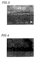
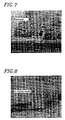
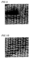
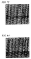
- Platinum metal thin film is a commonly used material for the a device electrode.
- the platinum metal thin film is subject to etching processes to form device patterns on silicon wafers.
- the best technique for platinum etching is a dry etching process, using chlorine-containing gases.
- the chlorine-containing gases react with the platinum metal to form non-volatile platinum-chloride-containing compounds, which removes platinum, but which leaves the platinum-chloride-containing compounds on other portions of the structure, or forms a fence along a photoresist side wall. Because these platinum-chloride-containing etching products are not volatile, they cannot be removed by a dynamic vacuum system. Wafer cleaning is necessary to remove the platinum-chloride-containing etching by-products from patterned metal oxide thin films.
Landscapes
- Cleaning Or Drying Semiconductors (AREA)
- Drying Of Semiconductors (AREA)
Applications Claiming Priority (2)
| Application Number | Priority Date | Filing Date | Title |
|---|---|---|---|
| US965581 | 1992-10-23 | ||
| US09/965,581 US6457479B1 (en) | 2001-09-26 | 2001-09-26 | Method of metal oxide thin film cleaning |
Publications (2)
| Publication Number | Publication Date |
|---|---|
| EP1306895A2 true EP1306895A2 (fr) | 2003-05-02 |
| EP1306895A3 EP1306895A3 (fr) | 2004-07-28 |
Family
ID=25510171
Family Applications (1)
| Application Number | Title | Priority Date | Filing Date |
|---|---|---|---|
| EP02021751A Withdrawn EP1306895A3 (fr) | 2001-09-26 | 2002-09-25 | Méthode de nettoyage d'une couche mince d'oxyde métallique |
Country Status (5)
| Country | Link |
|---|---|
| US (1) | US6457479B1 (fr) |
| EP (1) | EP1306895A3 (fr) |
| JP (1) | JP2003100712A (fr) |
| KR (1) | KR100491386B1 (fr) |
| TW (1) | TW553781B (fr) |
Families Citing this family (42)
| Publication number | Priority date | Publication date | Assignee | Title |
|---|---|---|---|---|
| US8103496B1 (en) | 2000-10-26 | 2012-01-24 | Cypress Semicondutor Corporation | Breakpoint control in an in-circuit emulation system |
| US6724220B1 (en) | 2000-10-26 | 2004-04-20 | Cyress Semiconductor Corporation | Programmable microcontroller architecture (mixed analog/digital) |
| US8176296B2 (en) | 2000-10-26 | 2012-05-08 | Cypress Semiconductor Corporation | Programmable microcontroller architecture |
| US8149048B1 (en) | 2000-10-26 | 2012-04-03 | Cypress Semiconductor Corporation | Apparatus and method for programmable power management in a programmable analog circuit block |
| US7765095B1 (en) | 2000-10-26 | 2010-07-27 | Cypress Semiconductor Corporation | Conditional branching in an in-circuit emulation system |
| US8160864B1 (en) | 2000-10-26 | 2012-04-17 | Cypress Semiconductor Corporation | In-circuit emulator and pod synchronized boot |
| JP2003115576A (ja) * | 2001-10-03 | 2003-04-18 | Matsushita Electric Ind Co Ltd | 電子デバイスの製造方法 |
| US7406674B1 (en) | 2001-10-24 | 2008-07-29 | Cypress Semiconductor Corporation | Method and apparatus for generating microcontroller configuration information |
| US8078970B1 (en) | 2001-11-09 | 2011-12-13 | Cypress Semiconductor Corporation | Graphical user interface with user-selectable list-box |
| US8042093B1 (en) | 2001-11-15 | 2011-10-18 | Cypress Semiconductor Corporation | System providing automatic source code generation for personalization and parameterization of user modules |
| US8069405B1 (en) | 2001-11-19 | 2011-11-29 | Cypress Semiconductor Corporation | User interface for efficiently browsing an electronic document using data-driven tabs |
| US7774190B1 (en) | 2001-11-19 | 2010-08-10 | Cypress Semiconductor Corporation | Sleep and stall in an in-circuit emulation system |
| US6971004B1 (en) | 2001-11-19 | 2005-11-29 | Cypress Semiconductor Corp. | System and method of dynamically reconfiguring a programmable integrated circuit |
| US7844437B1 (en) | 2001-11-19 | 2010-11-30 | Cypress Semiconductor Corporation | System and method for performing next placements and pruning of disallowed placements for programming an integrated circuit |
| US7770113B1 (en) | 2001-11-19 | 2010-08-03 | Cypress Semiconductor Corporation | System and method for dynamically generating a configuration datasheet |
| US8103497B1 (en) | 2002-03-28 | 2012-01-24 | Cypress Semiconductor Corporation | External interface for event architecture |
| US7308608B1 (en) | 2002-05-01 | 2007-12-11 | Cypress Semiconductor Corporation | Reconfigurable testing system and method |
| US7761845B1 (en) | 2002-09-09 | 2010-07-20 | Cypress Semiconductor Corporation | Method for parameterizing a user module |
| KR100532950B1 (ko) * | 2003-04-16 | 2005-12-02 | 주식회사 하이닉스반도체 | 웨이퍼 습식 세정 방법 |
| US7295049B1 (en) | 2004-03-25 | 2007-11-13 | Cypress Semiconductor Corporation | Method and circuit for rapid alignment of signals |
| US8069436B2 (en) | 2004-08-13 | 2011-11-29 | Cypress Semiconductor Corporation | Providing hardware independence to automate code generation of processing device firmware |
| US8286125B2 (en) | 2004-08-13 | 2012-10-09 | Cypress Semiconductor Corporation | Model for a hardware device-independent method of defining embedded firmware for programmable systems |
| US7332976B1 (en) | 2005-02-04 | 2008-02-19 | Cypress Semiconductor Corporation | Poly-phase frequency synthesis oscillator |
| US7400183B1 (en) | 2005-05-05 | 2008-07-15 | Cypress Semiconductor Corporation | Voltage controlled oscillator delay cell and method |
| US8089461B2 (en) | 2005-06-23 | 2012-01-03 | Cypress Semiconductor Corporation | Touch wake for electronic devices |
| US8085067B1 (en) | 2005-12-21 | 2011-12-27 | Cypress Semiconductor Corporation | Differential-to-single ended signal converter circuit and method |
| US8067948B2 (en) | 2006-03-27 | 2011-11-29 | Cypress Semiconductor Corporation | Input/output multiplexer bus |
| US8040266B2 (en) | 2007-04-17 | 2011-10-18 | Cypress Semiconductor Corporation | Programmable sigma-delta analog-to-digital converter |
| US8130025B2 (en) | 2007-04-17 | 2012-03-06 | Cypress Semiconductor Corporation | Numerical band gap |
| US9564902B2 (en) | 2007-04-17 | 2017-02-07 | Cypress Semiconductor Corporation | Dynamically configurable and re-configurable data path |
| US8092083B2 (en) | 2007-04-17 | 2012-01-10 | Cypress Semiconductor Corporation | Temperature sensor with digital bandgap |
| US8026739B2 (en) | 2007-04-17 | 2011-09-27 | Cypress Semiconductor Corporation | System level interconnect with programmable switching |
| US7737724B2 (en) | 2007-04-17 | 2010-06-15 | Cypress Semiconductor Corporation | Universal digital block interconnection and channel routing |
| US8516025B2 (en) | 2007-04-17 | 2013-08-20 | Cypress Semiconductor Corporation | Clock driven dynamic datapath chaining |
| US9720805B1 (en) | 2007-04-25 | 2017-08-01 | Cypress Semiconductor Corporation | System and method for controlling a target device |
| US8065653B1 (en) | 2007-04-25 | 2011-11-22 | Cypress Semiconductor Corporation | Configuration of programmable IC design elements |
| US8266575B1 (en) | 2007-04-25 | 2012-09-11 | Cypress Semiconductor Corporation | Systems and methods for dynamically reconfiguring a programmable system on a chip |
| US8049569B1 (en) | 2007-09-05 | 2011-11-01 | Cypress Semiconductor Corporation | Circuit and method for improving the accuracy of a crystal-less oscillator having dual-frequency modes |
| US9448964B2 (en) | 2009-05-04 | 2016-09-20 | Cypress Semiconductor Corporation | Autonomous control in a programmable system |
| US8128755B2 (en) * | 2010-03-03 | 2012-03-06 | L'air Liquide Societe Anonyme Pour L'etude Et L'exploitation Des Procedes Georges Claude | Cleaning solvent and cleaning method for metallic compound |
| KR101559847B1 (ko) * | 2014-01-10 | 2015-10-13 | 한국기계연구원 | 저온 소결법을 이용한 전극 제조방법 |
| KR101604400B1 (ko) | 2014-02-10 | 2016-03-18 | 한국기계연구원 | 저온 소결법을 이용한 전극 제조장치 |
Family Cites Families (17)
| Publication number | Priority date | Publication date | Assignee | Title |
|---|---|---|---|---|
| US5561082A (en) * | 1992-07-31 | 1996-10-01 | Kabushiki Kaisha Toshiba | Method for forming an electrode and/or wiring layer by reducing copper oxide or silver oxide |
| US5911837A (en) * | 1993-07-16 | 1999-06-15 | Legacy Systems, Inc. | Process for treatment of semiconductor wafers in a fluid |
| JPH07130702A (ja) * | 1993-11-08 | 1995-05-19 | Fujitsu Ltd | 白金又はパラジウムよりなる金属膜のパターニング方法 |
| US6030754A (en) * | 1996-02-05 | 2000-02-29 | Texas Instruments Incorporated | Photoresist removal without organic solvent following ashing operation |
| JP2836562B2 (ja) * | 1996-02-08 | 1998-12-14 | 日本電気株式会社 | 半導体ウェハのウェット処理方法 |
| US6045624A (en) * | 1996-09-27 | 2000-04-04 | Tokyo Electron Limited | Apparatus for and method of cleaning objects to be processed |
| EP0907203A3 (fr) * | 1997-09-03 | 2000-07-12 | Siemens Aktiengesellschaft | Méthode de structuration |
| US6004886A (en) * | 1997-10-30 | 1999-12-21 | National Science Council | Liquid phase deposition method for forming silicon dioxide film on HGCDTE or other II-VI semiconductor substrate |
| US6211126B1 (en) * | 1997-12-23 | 2001-04-03 | Advanced Technology Materials, Inc. | Formulations including a 1, 3-dicarbonyl compound chelating agent for stripping residues from semiconductor substrates |
| KR100305213B1 (ko) * | 1997-12-30 | 2001-11-02 | 박종섭 | 반도체소자의세정방법 |
| US6105588A (en) * | 1998-05-27 | 2000-08-22 | Micron Technology, Inc. | Method of resist stripping during semiconductor device fabrication |
| KR100464305B1 (ko) * | 1998-07-07 | 2005-04-13 | 삼성전자주식회사 | 에챈트를이용한pzt박막의청소방법 |
| US6107202A (en) * | 1998-09-14 | 2000-08-22 | Taiwan Semiconductor Manufacturing Company | Passivation photoresist stripping method to eliminate photoresist extrusion after alloy |
| DE19935131B4 (de) * | 1999-07-27 | 2006-01-26 | Infineon Technologies Ag | Verfahren zur Beseitigung von Redepositionen von einem Wafer |
| JP2001100436A (ja) * | 1999-09-28 | 2001-04-13 | Mitsubishi Gas Chem Co Inc | レジスト剥離液組成物 |
| US6475966B1 (en) * | 2000-02-25 | 2002-11-05 | Shipley Company, L.L.C. | Plasma etching residue removal |
| JP2001351898A (ja) * | 2000-06-07 | 2001-12-21 | Nec Corp | 半導体装置の製造方法 |
-
2001
- 2001-09-26 US US09/965,581 patent/US6457479B1/en not_active Expired - Fee Related
-
2002
- 2002-09-17 JP JP2002270820A patent/JP2003100712A/ja active Pending
- 2002-09-23 TW TW091121770A patent/TW553781B/zh not_active IP Right Cessation
- 2002-09-25 EP EP02021751A patent/EP1306895A3/fr not_active Withdrawn
- 2002-09-26 KR KR10-2002-0058366A patent/KR100491386B1/ko not_active Expired - Fee Related
Also Published As
| Publication number | Publication date |
|---|---|
| US6457479B1 (en) | 2002-10-01 |
| TW553781B (en) | 2003-09-21 |
| KR20030027737A (ko) | 2003-04-07 |
| JP2003100712A (ja) | 2003-04-04 |
| EP1306895A3 (fr) | 2004-07-28 |
| KR100491386B1 (ko) | 2005-05-24 |
Similar Documents
| Publication | Publication Date | Title |
|---|---|---|
| US6457479B1 (en) | Method of metal oxide thin film cleaning | |
| US8058181B1 (en) | Method for post-etch cleans | |
| US5346586A (en) | Method for selectively etching polysilicon to gate oxide using an insitu ozone photoresist strip | |
| US6926014B2 (en) | Method for cleaning a plasma chamber | |
| KR101827020B1 (ko) | 고애스펙트비 나노구조들의 패턴 붕괴를 저감시키는 방법 | |
| JPH11260785A (ja) | フォトレジスト材料とエッチング残留物の除去方法 | |
| US20050066994A1 (en) | Methods for cleaning processing chambers | |
| JPH08153710A (ja) | 半導体装置の製造方法 | |
| JP2002151484A (ja) | エッチング後の洗浄処理法 | |
| JP2008218867A (ja) | 半導体装置の製造方法 | |
| JPH09102483A (ja) | 半導体基板上にシリコン材料の上部構造体を形成する製造方法 | |
| JPH09298199A (ja) | 半導体装置及びその製造方法 | |
| US6066572A (en) | Method of removing carbon contamination on semiconductor substrate | |
| JP2003023072A (ja) | 半導体装置の製造方法および半導体装置の製造装置 | |
| EP1200987A2 (fr) | Procede de preparation d'un substrat semi-conducteur destine a subir un traitement au siliciure ulterieur | |
| JP2003520446A (ja) | 酸化物がエッチングされないようにした残渣除去方法 | |
| US6010949A (en) | Method for removing silicon nitride in the fabrication of semiconductor devices | |
| JPH0766168A (ja) | 半導体製造方法および半導体製造装置 | |
| TW554389B (en) | Method for plasma etching of Ir-Ta-O electrode and for post-etch cleaning | |
| JPH09190994A (ja) | ケイ酸残留物の生成を防止のためのフッ酸処理後の脱イオン水/オゾン洗浄 | |
| JPH0451520A (ja) | 半導体装置の製造方法 | |
| KR100196508B1 (ko) | 반도체 장치의 폴리실리콘막 세정방법 | |
| TW541358B (en) | Method for dry cleaning metal etching chamber | |
| JPH10116806A (ja) | 半導体ウエハの洗浄方法 | |
| JP2000260749A (ja) | ドライエッチング装置及びそのプラズマクリーニング方法 |
Legal Events
| Date | Code | Title | Description |
|---|---|---|---|
| PUAI | Public reference made under article 153(3) epc to a published international application that has entered the european phase |
Free format text: ORIGINAL CODE: 0009012 |
|
| AK | Designated contracting states |
Designated state(s): AT BE BG CH CY CZ DE DK EE ES FI FR GB GR IE IT LI LU MC NL PT SE SK TR |
|
| AX | Request for extension of the european patent |
Extension state: AL LT LV MK RO SI |
|
| PUAL | Search report despatched |
Free format text: ORIGINAL CODE: 0009013 |
|
| AK | Designated contracting states |
Kind code of ref document: A3 Designated state(s): AT BE BG CH CY CZ DE DK EE ES FI FR GB GR IE IT LI LU MC NL PT SE SK TR |
|
| AX | Request for extension of the european patent |
Extension state: AL LT LV MK RO SI |
|
| 17P | Request for examination filed |
Effective date: 20050114 |
|
| AKX | Designation fees paid |
Designated state(s): DE FR GB |
|
| 17Q | First examination report despatched |
Effective date: 20061123 |
|
| STAA | Information on the status of an ep patent application or granted ep patent |
Free format text: STATUS: THE APPLICATION IS DEEMED TO BE WITHDRAWN |
|
| 18D | Application deemed to be withdrawn |
Effective date: 20090818 |