EP1306900A2 - Chipgrosse Gehäuse gestapelt auf Falt-Verbindung für Vertikalmontage auf Substraten - Google Patents
Chipgrosse Gehäuse gestapelt auf Falt-Verbindung für Vertikalmontage auf Substraten Download PDFInfo
- Publication number
- EP1306900A2 EP1306900A2 EP01000785A EP01000785A EP1306900A2 EP 1306900 A2 EP1306900 A2 EP 1306900A2 EP 01000785 A EP01000785 A EP 01000785A EP 01000785 A EP01000785 A EP 01000785A EP 1306900 A2 EP1306900 A2 EP 1306900A2
- Authority
- EP
- European Patent Office
- Prior art keywords
- interconnector
- ports
- coupling members
- center
- electrical
- Prior art date
- Legal status (The legal status is an assumption and is not a legal conclusion. Google has not performed a legal analysis and makes no representation as to the accuracy of the status listed.)
- Withdrawn
Links
Images


Classifications
-
- H—ELECTRICITY
- H10—SEMICONDUCTOR DEVICES; ELECTRIC SOLID-STATE DEVICES NOT OTHERWISE PROVIDED FOR
- H10W—GENERIC PACKAGES, INTERCONNECTIONS, CONNECTORS OR OTHER CONSTRUCTIONAL DETAILS OF DEVICES COVERED BY CLASS H10
- H10W72/00—Interconnections or connectors in packages
-
- H—ELECTRICITY
- H05—ELECTRIC TECHNIQUES NOT OTHERWISE PROVIDED FOR
- H05K—PRINTED CIRCUITS; CASINGS OR CONSTRUCTIONAL DETAILS OF ELECTRIC APPARATUS; MANUFACTURE OF ASSEMBLAGES OF ELECTRICAL COMPONENTS
- H05K1/00—Printed circuits
- H05K1/18—Printed circuits structurally associated with non-printed electric components
- H05K1/189—Printed circuits structurally associated with non-printed electric components characterised by the use of flexible or folded printed circuits
-
- H—ELECTRICITY
- H10—SEMICONDUCTOR DEVICES; ELECTRIC SOLID-STATE DEVICES NOT OTHERWISE PROVIDED FOR
- H10W—GENERIC PACKAGES, INTERCONNECTIONS, CONNECTORS OR OTHER CONSTRUCTIONAL DETAILS OF DEVICES COVERED BY CLASS H10
- H10W70/00—Package substrates; Interposers; Redistribution layers [RDL]
- H10W70/60—Insulating or insulated package substrates; Interposers; Redistribution layers
- H10W70/611—Insulating or insulated package substrates; Interposers; Redistribution layers for connecting multiple chips together
-
- H—ELECTRICITY
- H10—SEMICONDUCTOR DEVICES; ELECTRIC SOLID-STATE DEVICES NOT OTHERWISE PROVIDED FOR
- H10W—GENERIC PACKAGES, INTERCONNECTIONS, CONNECTORS OR OTHER CONSTRUCTIONAL DETAILS OF DEVICES COVERED BY CLASS H10
- H10W70/00—Package substrates; Interposers; Redistribution layers [RDL]
- H10W70/60—Insulating or insulated package substrates; Interposers; Redistribution layers
- H10W70/67—Insulating or insulated package substrates; Interposers; Redistribution layers characterised by their insulating layers or insulating parts
- H10W70/688—Flexible insulating substrates
-
- H—ELECTRICITY
- H10—SEMICONDUCTOR DEVICES; ELECTRIC SOLID-STATE DEVICES NOT OTHERWISE PROVIDED FOR
- H10W—GENERIC PACKAGES, INTERCONNECTIONS, CONNECTORS OR OTHER CONSTRUCTIONAL DETAILS OF DEVICES COVERED BY CLASS H10
- H10W74/00—Encapsulations, e.g. protective coatings
- H10W74/10—Encapsulations, e.g. protective coatings characterised by their shape or disposition
- H10W74/111—Encapsulations, e.g. protective coatings characterised by their shape or disposition the semiconductor body being completely enclosed
- H10W74/129—Encapsulations, e.g. protective coatings characterised by their shape or disposition the semiconductor body being completely enclosed forming a chip-scale package [CSP]
-
- H—ELECTRICITY
- H10—SEMICONDUCTOR DEVICES; ELECTRIC SOLID-STATE DEVICES NOT OTHERWISE PROVIDED FOR
- H10W—GENERIC PACKAGES, INTERCONNECTIONS, CONNECTORS OR OTHER CONSTRUCTIONAL DETAILS OF DEVICES COVERED BY CLASS H10
- H10W90/00—Package configurations
-
- H—ELECTRICITY
- H10—SEMICONDUCTOR DEVICES; ELECTRIC SOLID-STATE DEVICES NOT OTHERWISE PROVIDED FOR
- H10W—GENERIC PACKAGES, INTERCONNECTIONS, CONNECTORS OR OTHER CONSTRUCTIONAL DETAILS OF DEVICES COVERED BY CLASS H10
- H10W70/00—Package substrates; Interposers; Redistribution layers [RDL]
- H10W70/60—Insulating or insulated package substrates; Interposers; Redistribution layers
-
- H—ELECTRICITY
- H10—SEMICONDUCTOR DEVICES; ELECTRIC SOLID-STATE DEVICES NOT OTHERWISE PROVIDED FOR
- H10W—GENERIC PACKAGES, INTERCONNECTIONS, CONNECTORS OR OTHER CONSTRUCTIONAL DETAILS OF DEVICES COVERED BY CLASS H10
- H10W72/00—Interconnections or connectors in packages
- H10W72/071—Connecting or disconnecting
- H10W72/072—Connecting or disconnecting of bump connectors
- H10W72/07251—Connecting or disconnecting of bump connectors characterised by changes in properties of the bump connectors during connecting
-
- H—ELECTRICITY
- H10—SEMICONDUCTOR DEVICES; ELECTRIC SOLID-STATE DEVICES NOT OTHERWISE PROVIDED FOR
- H10W—GENERIC PACKAGES, INTERCONNECTIONS, CONNECTORS OR OTHER CONSTRUCTIONAL DETAILS OF DEVICES COVERED BY CLASS H10
- H10W72/00—Interconnections or connectors in packages
- H10W72/20—Bump connectors, e.g. solder bumps or copper pillars; Dummy bumps; Thermal bumps
-
- H—ELECTRICITY
- H10—SEMICONDUCTOR DEVICES; ELECTRIC SOLID-STATE DEVICES NOT OTHERWISE PROVIDED FOR
- H10W—GENERIC PACKAGES, INTERCONNECTIONS, CONNECTORS OR OTHER CONSTRUCTIONAL DETAILS OF DEVICES COVERED BY CLASS H10
- H10W90/00—Package configurations
- H10W90/701—Package configurations characterised by the relative positions of pads or connectors relative to package parts
- H10W90/721—Package configurations characterised by the relative positions of pads or connectors relative to package parts of bump connectors
- H10W90/722—Package configurations characterised by the relative positions of pads or connectors relative to package parts of bump connectors between stacked chips
Definitions
- the present invention is related in general to the field of semiconductor devices and processes, and more specifically to structure and processes of chip-scale packages stacked onto interconnecting film for vertical assembly onto substrates.
- the chips usually of different types, are attached to leadframe chip pads; their input/output terminals are wire bonded to the inner lead of the leadframe.
- other leads are used under or over the semiconductor chips in order to interconnect terminals which cannot be reached by long-spanned wire bonding.
- the assembly is encapsulated in a plastic package. In both of these examples, the end products are large, since the chips are placed side by side. In contrast, today's applications require ever shrinking semiconductor products, and board consumption is to be minimized.
- U.S. Patent No. 5,438,224, Aug. 1, 1995 discloses an integrated circuit (IC) package with a stacked IC chip arrangement placed on a circuit substrate. Two chips are positioned face to face, with a substrate made of tape-automated bonding tape or flex circuit interposed between the chips to provide electrical connection among the terminals of the flip chip and external circuitry; a separate mechanical support is needed for the assembly. In addition to this cost, fabrication is difficult due to the lack of rigid support for the chips.
- a vertical stack of semiconductor devices is formed by folding a strip-like flexible interconnector assembled with integrated circuit chips, packages and/or passive components and attaching coupling members solderable to other parts.
- the invention describes a semiconductor assembly comprising a strip-like flexible interconnector of electrically insulating material having first and second surfaces.
- the interconnector has on its first surface electrically conductive lines for connecting a plurality of semiconductor devices formed on the first surface adjacent to each other.
- the interconnector further has electrically conductive paths extending from its first surface to its second surface, forming electrical ports on the second surface.
- the ports comprise first and second pluralities, the first plurality ports spaced apart by less, center to center, than said second plurality ports are spaced apart, center to center.
- the interconnector is folded so that said adjacent semiconductor devices are stacked on top of each other.
- the assembly comprises at least one additional semiconductor device, which has a plurality of first electrical coupling members, with these first coupling members attached to the first plurality ports. Finally, a plurality of second electrical coupling members is attached to the second plurality ports and these coupling members are suitable for attachment to other parts.
- a preferred embodiment comprises devices of small geometries such as chip-scale and chip-size packages.
- the flexible interconnector enables the transition from the fine-pitch land pads for the attached discreet devices to the customer-desired pitch for the solderable coupling members.
- the discreet devices include fine-pitch, bumped chip-scale packages and fine-pitch flipped, bumped chips.
- Another aspect of the present invention is to provide a high production throughput by employing multiple footprint techniques for active and passive components.
- Another aspect of the invention is to improve electrical product performance by minimizing parasitic resistances and inductances.
- Another aspect of the invention is to provide high quality control and reliability assurance through in-process control at no extra cost.
- Another aspect of the invention is to introduce assembly concepts for thin profiles and reliability which are flexible so that they can be applied to many families of semiconductor products, and are general so that they can be applied to several future generations of products.
- Another aspect of the invention is to minimize the cost of capital investment and the movement of parts and product in the equipment.
- a first embodiment of the invention combines two single or dual-chip packages with passive components, or with multiple fine-pitch chip-scale packages, or with multiple bumped and flipped chips.
- a second embodiment of the invention combines three single or dual-chip packages with a third package, which has been fabricated and tested separately.
- a third embodiment of the invention combines three single or dual-chip packages with passive components, or with multiple fine-pitch chip-scale packages, or multiple bumped and flipped chips.
- a fourth embodiment of the invention combines three single or dual-chip packages.
- the invention further provides for a variety of other different combinations.
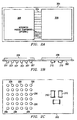
- FIG. I1A is a schematic top view of the partially assembled interconnector according to System and Flow I of the invention.
- FIG. I1B is a schematic cross section of the partially assembled interconnector according to System and Flow I of the invention.
- FIG. I1C is a schematic bottom view of the partially assembled interconnector according to System and Flow I of the invention.
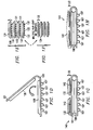
- FIG. I2 is a schematic cross section of the partially assembled interconnector in the process of folding, according to System and Flow I of the invention.
- FIG. I3A is a schematic cross section of a plurality of fine-pitch chip-scale packages prepared for attachment onto the folded interconnector of FIG. I2.
- FIG. I3B is a schematic cross section of a plurality of integrated circuit chips prepared for attachment onto the folded interconnector of FIG. I2.
- FIG. I4A is a schematic cross section of the fully assembled vertical device stack including the fine-pitch chip-scale packages of FIG. I3A.
- FIG. I4B is a schematic cross section of the fully assembled vertical device stack including the integrated circuit chips of FIG. I3B, with optional underfilling and/or encapsulation.
- FIG. II1A is a schematic top view of the partially assembled interconnector according to System and Flow II of the invention.
- FIG. II1B is a schematic cross section of the partially assembled interconnector according to System and Flow II of the invention.
- FIG. II1C is a schematic bottom view of the partially assembled interconnector according to System and Flow II of the invention.
- FIG. II2 is a schematic cross section of the partially assembled interconnector in the process of folding, according to System and Flow II of the invention.
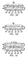
- FIG. II4A is a schematic cross section of the fully assembled vertical device stack including two packages and passive components.
- FIG. II4B is a schematic cross section of the fully assembled vertical device stack including a third package, which has bee fabricated and tested separately.
- FIG. II4C is a schematic cross section of the fully assembled vertical stack including three packages and passive components.
- FIG. II4D is a schematic cross section of the fully assembled vertical stack including three packages assembled on opposite surfaces of the interconnector.
- FIG. II4E is a schematic cross section of the fully assembled vertical stack illustrating an additional example of assembly options provided by the invention.
- FIGs. I1A through I4B System and Flow II are illustrated in FIGs. II1A through II4E.
- FIG. I1A shows schematically the top view of a rectangular strip-like interconnector 101. It is made of electrically insulating material which is flexible. A preferred choice is a polyimide film in the thickness range from about 40 to 80 ⁇ m; in some instances, it may be thicker. Given enough flexibility, other suitable materials include PCB resin, FR-4 (which is an epoxy resin), or a cyanate ester resin. These materials are commercially available from several sources; in the U.S.A., companies include 3-M and Sheldahl; in Japan, Shinko, Shindo, Sumitomo, and Mitsui; and in Hongkong, Compass.
- This interconnector has two surfaces; FIG. I1C depicts, in bottom view, the first surface 102, while FIG. I1A depicts, in top view, the second surface 103.
- Integral with the interconnector 101 is a plurality of electrically conductive lines 104 (they are depicted, as an example, in the top view of FIG. I1A). These conductive lines 104 are usually patterned from a thin metal foil, preferably between about 15 and 40 ⁇ m thick. Suitable materials include copper, copper alloys, gold, silver, palladium, platinum, and stacked of nickel/gold and nickel/ palladium. These conductive lines form on the first surface 102 a first array of electrical entry ports 105 and a second array of exit ports 106. As FIG. I1C shows, these arrays are grouped in separate areas of the interconnector; the entry ports 105 are actually depicted in multiple arrays.
- the entry ports 105 are spaced apart by less, center to center, than the exit ports 106 are spaced apart, center to center. While the present invention can be applied to any pitch of the entry or exit ports, preferably, these fine-pitched entry ports 105 are spaced apart from each other by less than 100 ⁇ m center to center. In contrast, the relatively wide-pitched exit ports 106 are typically spaced apart considerably more than 100 ⁇ m center to center. Since the exit ports 106 provide the attachment sites for the coupling members to other parts, their convenient spacing satisfies a desire often expressed by customers, namely to be provided with solder ball attachment sites convenient for semiconductor board assembly. Frequently, the exit ports 106 provide a common footprint to industry standards for chip-scale packages.
- Entry ports 105 are typically made of copper, often with a protective flash of gold. Exits ports 106 have to be solderable and thus have to insure reliable wetting. They may be covered by layers of a refractory metal (such as chromium, molybdenum, titanium, tungsten, or titanium/ tungsten alloy) and a noble metal (such as gold, palladium, platinum or platinum-rich alloy, silver or silver alloy).
- a refractory metal such as chromium, molybdenum, titanium, tungsten, or titanium/ tungsten alloy
- a noble metal such as gold, palladium, platinum or platinum-rich alloy, silver or silver alloy.
- the interconnector also has electrically conductive paths extending through the interconnector from one surface to the opposite surface.
- the mechanical flexibility of such interconnectors also helps preventing solder ball cracking under mechanical stress due to thermal cycling.
- the interconnector is preferably made of compliant material, such as tape, KaptonTM film, polyimide, or other plastic material, and may contain single or multiple layers of patterned conductors. In this fashion, the flexibility of the base material provides a stress buffer between the thermally mismatched semiconductor chip and the P.C. board, and will relieve some of the strain that develops in the chip solder balls in thermal cycling.
- an interconnector may be made of epoxies, FR-4, FR-5, or BT resin.
- Interconnectors with conductive through-paths are commercially available; for instance Novaclad® and ViaGrid® from Sheldahl, Inc., Northfield, MN. They are typically fabricated by laminating alternative films of electrically insulating and electrically conducting materials into one coherent layer. Connections through individual insulating films are made by laser drilling and metal refilling or plating, and patterning of the conductive films is achieved by ablation or etching. There are numerous designs and variations of interconnectors available.
- solder balls 107 are selected from a group consisting of pure tin, tin alloys including tin/copper, tin/indium, tin/silver, tin/ bismuth, tin/lead, and conductive adhesive compounds.
- solder "ball” does not imply that the solder contacts are necessarily spherical; they may have various forms, such as semispherical, half-dome, truncated cone, or generally bump, or a cylinder with straight, concave or convex outlines.
- the exact shape is a function of the deposition technique (such as evaporation, plating, or prefabricated units) and reflow technique (such as infrared or radiant heat), and the material composition.
- reflow technique such as infrared or radiant heat
- the diameter of the solder balls ranges from 0.1 to 0.5 mm, but can be significantly larger.
- FIG. I1A Further shown in the top view of FIG. I1A are encapsulated devices 108; they are depicted in cross section in FIG. I1B. Examples for such devices are MicroStar TM Ball Grid Arrays (BGAs) and MicroStarJuniorTM packages fabricated by Texas Instruments Incorporated, Dallas, Texas, U.S.A. These devices comprise integrated circuit (IC) chips attached to the interconnector film, wire bonding and transfer molded packages.
- IC integrated circuit
- the electrically conductive lines 104 indicated in FIG. I1A may contain at least one passive electrical component (not shown in FIG. I1A) integrated into the conductive lines. Examples include resistors, capacitors, inductors, distributed components, and networks of passive components and interconnected structures. Fabrication methods for these integrated components have recently been described in U.S. Patent Application # 60/244,673, filed on 10/31/2000 (Pritchett et al., "Plastic Chip-Scale Package having Integrated Passive Components”), which is herewith incorporated by reference.
- the flexible interconnector strip 101 is folded at the region 120 of the integrated conductive lines between the adjacent areas of the entry ports and exit ports.
- the folding is such that the entry ports face in one direction while the exit ports face in the opposite direction.
- the package bodies 108 touch each other, resulting in a vertically stacked assembly having approximately the outline of a chip-scale package. If desired, they package bodies can be glued together in order to render the tight stacking permanent.
- FIGs. I3A and I3B illustrate how the entry ports can be populated with semiconductor devices.
- FIG. I3A depicts, in schematic cross section, multiple chip-scale devices 130, packaged in an encapsulation 131 and having a plurality of fine-pitch electrical coupling members 132. These coupling members may consist of solder "balls" made of pure tin, a tin alloy as listed above, or a conductive adhesive compound.
- the pattern of the coupling members 132 is mirror-imaging the pattern of the interconnector entry ports.
- the fine-pitch coupling members 132 of chip-scale devices 130 are attached by surface mounting to the entry ports of the interconnector 101.
- the result is an assembly of chip-scale packages, generally designated 140, stacked vertically and having a plurality of coupling members 107 suitable for attachment to other, outside parts.
- FIG. I3B depicts, in schematic cross section, multiple un-encapsulated IC chips 133, prepared for flip-chip assembly by having a plurality of fine-pitch electrical coupling members 134.
- These coupling members may consist either of solder "balls" (made of pure tin, tin alloys as listed above, or a conductive adhesive compound) or of metal bumps selected from a group consisting of gold, copper, copper alloy, or layered copper/nickel/palladium.
- solder "balls” made of pure tin, tin alloys as listed above, or a conductive adhesive compound
- metal bumps selected from a group consisting of gold, copper, copper alloy, or layered copper/nickel/palladium.
- Another option is z-axis conductive epoxy.
- the bumps have various shapes, for example rectangular, square, round, or half-dome.
- the method of attaching the coupling members 134 to the entry ports of the interconnector is a thermo-compression bonding technique based on metal interdiffusion, as has been practiced previously in the tape-automated-bonding (TAB) fabrication method.
- the preferred technique for the present invention is a gang-bonding technique for array assembly. This technique has the advantage of fast and low-cost operation while resulting in high quality, reliable attachments.
- the automated apparatus is commercially available from Shinkawa Corporation, Japan.
- FIG. I4B shows as the result an assembly, generally designated 141, of flipped chips 133 and encapsulated devices 108, stacked vertically; the assembly further has a plurality of coupling members 107 suitable for attachment to other, outside parts.
- FIG. I4A shows that the packages 131 of devices 130 are spaced apart from the interconnector 101 by gaps 142.
- the solder balls 132 extend across the gaps, connecting to the interconnector. It is an advantage of this invention to choose the materials so that the significant difference in the coefficient of thermal expansion (CTE) between the semiconductor material of the IC chips and the material typically used for the interconnector can be minimized. It is, therefore, usually not necessary in the assembly of FIG. I4A to strengthen the solder joints (without affecting the electrical connection) by filling the gap 142 with a polymeric material which encapsulates the bumps and fills any space in the gap between the package and the interconnector ("underfilling" method).
- CTE coefficient of thermal expansion
- This method of underfilling may, however, be appropriate for the assembly depicted in FIG. I4B.
- This underfilling material, together with some encapsulating material, is indicated by the schematic outline 142 in FIG. I4B.
- the encapsulant is typically applied after completion of the assembly.
- a polymeric precursor, sometimes referred to as the "underfill” is dispensed onto the substrate adjacent to the chip and is pulled into the gap by capillary forces.
- the polymeric precursor comprises an epoxy-based material filled with silica and anhydrides.
- the precursor is then heated, polymerized and "cured” to form the encapsulant.
- the underfilling method preferred by this invention has been described in U.S. Patent Application # 60/084,440, filed on 05/06/98 (Thomas, "Low Stress Method and Apparatus of Underfilling Flip-Chip Electronic Devices").
- FIG. II1A shows schematically the top view of a rectangular strip-like interconnector 201, FIG. II1B its cross section, and FIG. II1C the bottom view.
- the descriptions for materials, processes, conductive lines 204, exit ports 206, optional integrated passive electrical components, solder balls 207, and packaged devices 208 are analogous to the descriptions in FIGs. I1A, I1B, and I1C.
- the significant difference is depicted in FIGs. II1B and II1C by the discreet passive components 210 attached to the first surface 202 of the interconnector 201. Consequently, the pattern of the entry ports in FIG. II1C is significantly simplified compared to the pattern in FIG. I1C. It is not specifically highlighted in FIG. II1C; it is implicit in the customized attachment the passive components 210.
- the folding of flexible interconnector strip 201 at the region 220 of the integrated conductive lines between adjacent areas of the entry and exit ports, as illustrated in FIG. II2, is analogous to the folding of interconnector 101 in FIG. I2.
- the package bodies 208 touch each other, resulting in a vertically stacked assembly having approximately the outline of a chip-scale package. If desired, they package bodies can be glued together in order to render the tight stacking permanent.
- FIG. II4A It is an assembly, generally designated 240, of chip-scale packages 208 and discreet passive electrical components 210 stacked vertically and having a plurality of coupling members 207 (usually solder balls) suitable for attachment to other parts.
- This assembly in FIG. II4A like the analogous assemblies in FIGs. I4A and I4B, represents an example of the fist embodiment of this invention:
- the material of the semiconductor chip may comprise silicon, silicon germanium, gallium arsenide, or any other semiconductor material used in manufacturing. It is therefore intended that the appended claims encompass any such modifications or embodiments.
Landscapes
- Engineering & Computer Science (AREA)
- Microelectronics & Electronic Packaging (AREA)
- Wire Bonding (AREA)
- Credit Cards Or The Like (AREA)
- Structures For Mounting Electric Components On Printed Circuit Boards (AREA)
Applications Claiming Priority (2)
| Application Number | Priority Date | Filing Date | Title |
|---|---|---|---|
| US25852500P | 2000-12-28 | 2000-12-28 | |
| US258525 | 2000-12-28 |
Publications (2)
| Publication Number | Publication Date |
|---|---|
| EP1306900A2 true EP1306900A2 (de) | 2003-05-02 |
| EP1306900A3 EP1306900A3 (de) | 2005-07-06 |
Family
ID=22980939
Family Applications (1)
| Application Number | Title | Priority Date | Filing Date |
|---|---|---|---|
| EP01000785A Withdrawn EP1306900A3 (de) | 2000-12-28 | 2001-12-20 | Chipgrosse Gehäuse gestapelt auf Falt-Verbindung für Vertikalmontage auf Substraten |
Country Status (5)
| Country | Link |
|---|---|
| US (1) | US20020114143A1 (de) |
| EP (1) | EP1306900A3 (de) |
| JP (1) | JP2002237568A (de) |
| KR (1) | KR20020055573A (de) |
| TW (1) | TW531815B (de) |
Cited By (2)
| Publication number | Priority date | Publication date | Assignee | Title |
|---|---|---|---|---|
| WO2008055708A3 (de) * | 2006-11-09 | 2008-07-10 | Fraunhofer Ges Forschung | Mikroelektronische baugruppe und verfahren zum herstellen einer mikroelektronischen baugruppe |
| WO2008103518A1 (en) * | 2007-02-20 | 2008-08-28 | Micron Technology, Inc. | Packaged ic device comprising an embedded flex circuit, and methods of making same |
Families Citing this family (63)
| Publication number | Priority date | Publication date | Assignee | Title |
|---|---|---|---|---|
| US6914324B2 (en) | 2001-10-26 | 2005-07-05 | Staktek Group L.P. | Memory expansion and chip scale stacking system and method |
| US6940729B2 (en) | 2001-10-26 | 2005-09-06 | Staktek Group L.P. | Integrated circuit stacking system and method |
| US7656678B2 (en) | 2001-10-26 | 2010-02-02 | Entorian Technologies, Lp | Stacked module systems |
| US7371609B2 (en) | 2001-10-26 | 2008-05-13 | Staktek Group L.P. | Stacked module systems and methods |
| US6956284B2 (en) | 2001-10-26 | 2005-10-18 | Staktek Group L.P. | Integrated circuit stacking system and method |
| US7310458B2 (en) | 2001-10-26 | 2007-12-18 | Staktek Group L.P. | Stacked module systems and methods |
| US20030234443A1 (en) | 2001-10-26 | 2003-12-25 | Staktek Group, L.P. | Low profile stacking system and method |
| US20060255446A1 (en) | 2001-10-26 | 2006-11-16 | Staktek Group, L.P. | Stacked modules and method |
| US7485951B2 (en) | 2001-10-26 | 2009-02-03 | Entorian Technologies, Lp | Modularized die stacking system and method |
| KR100460062B1 (ko) * | 2002-04-23 | 2004-12-04 | 주식회사 하이닉스반도체 | 멀티 칩 패키지 및 그 제조 방법 |
| US7017638B2 (en) * | 2002-07-08 | 2006-03-28 | Intel Corporation | Forming folded-stack packaged device using vertical progression folding tool |
| KR100587055B1 (ko) * | 2002-09-03 | 2006-06-07 | 주식회사 하이닉스반도체 | Bga 패키지 스택의 싱규레이션을 위한 플렉시블 테이프 및 그를 사용한 bga 패키지 제조방법 |
| KR100480437B1 (ko) | 2002-10-24 | 2005-04-07 | 삼성전자주식회사 | 반도체 칩 패키지 적층 모듈 |
| KR20040059741A (ko) * | 2002-12-30 | 2004-07-06 | 동부전자 주식회사 | 반도체용 멀티 칩 모듈의 패키징 방법 |
| KR20040059742A (ko) * | 2002-12-30 | 2004-07-06 | 동부전자 주식회사 | 반도체용 멀티 칩 모듈의 패키징 방법 |
| US20040156177A1 (en) * | 2003-02-12 | 2004-08-12 | Matsushita Electric Industrial Co., Ltd. | Package of electronic components and method for producing the same |
| US6995465B2 (en) * | 2003-06-04 | 2006-02-07 | Intel Corporation | Silicon building block architecture with flex tape |
| US6992376B2 (en) * | 2003-07-17 | 2006-01-31 | Intel Corporation | Electronic package having a folded package substrate |
| US7542304B2 (en) | 2003-09-15 | 2009-06-02 | Entorian Technologies, Lp | Memory expansion and integrated circuit stacking system and method |
| JP4285339B2 (ja) * | 2004-06-15 | 2009-06-24 | パナソニック株式会社 | 回路モジュールおよび回路モジュールの製造方法 |
| JP4196901B2 (ja) * | 2004-08-11 | 2008-12-17 | ソニー株式会社 | 電子回路装置 |
| WO2006028643A2 (en) * | 2004-09-03 | 2006-03-16 | Staktek Group L.P. | Circuit module system and method |
| CN100347856C (zh) * | 2004-09-27 | 2007-11-07 | 赵建铭 | 封装有多个晶片的封装件及其封装方法 |
| US7459772B2 (en) * | 2004-09-29 | 2008-12-02 | Actel Corporation | Face-to-face bonded I/O circuit die and functional logic circuit die system |
| US20100020515A1 (en) * | 2005-03-08 | 2010-01-28 | Smart Modular Technologies, Inc. | Method and system for manufacturing micro solid state drive devices |
| TW200639507A (en) * | 2005-05-11 | 2006-11-16 | Au Optronics Corp | Backlight structure and lighting module therefor |
| US7033861B1 (en) * | 2005-05-18 | 2006-04-25 | Staktek Group L.P. | Stacked module systems and method |
| KR100660900B1 (ko) | 2005-12-21 | 2006-12-26 | 삼성전자주식회사 | 폴드형 칩 스택 패키지 및 그 패키지의 형성방법 |
| JP2007266540A (ja) * | 2006-03-30 | 2007-10-11 | Elpida Memory Inc | 半導体装置及びその製造方法 |
| US20110090413A1 (en) * | 2006-08-18 | 2011-04-21 | Industrial Technology Research Institute | 3-dimensional image display |
| TWI378747B (en) * | 2006-08-18 | 2012-12-01 | Ind Tech Res Inst | Flexible electronic assembly |
| US7514773B2 (en) * | 2006-08-31 | 2009-04-07 | Intel Corporation | Systems and arrangements for interconnecting integrated circuit dies |
| US7417310B2 (en) * | 2006-11-02 | 2008-08-26 | Entorian Technologies, Lp | Circuit module having force resistant construction |
| US8350382B2 (en) | 2007-09-21 | 2013-01-08 | Infineon Technologies Ag | Semiconductor device including electronic component coupled to a backside of a chip |
| US7790502B2 (en) * | 2007-12-10 | 2010-09-07 | Honeywell International Inc. | Method of manufacturing flexible semiconductor assemblies |
| JP5012612B2 (ja) * | 2008-03-26 | 2012-08-29 | 日本電気株式会社 | 半導体デバイスの実装構造体及び実装構造体を用いた電子機器 |
| JP2010016339A (ja) * | 2008-06-03 | 2010-01-21 | Nippon Mektron Ltd | 多層フレキシブルプリント回路基板を用いたモジュールおよびその製造方法 |
| KR101429722B1 (ko) * | 2008-07-28 | 2014-09-25 | 삼성전자주식회사 | 적층된 칩들을 갖는 전자 장치 형성 방법 |
| US7869206B2 (en) | 2008-09-05 | 2011-01-11 | Apple Inc. | Handheld computing device |
| US7697281B2 (en) | 2008-09-05 | 2010-04-13 | Apple Inc. | Handheld computing device |
| US9165841B2 (en) | 2008-09-19 | 2015-10-20 | Intel Corporation | System and process for fabricating semiconductor packages |
| US9164404B2 (en) * | 2008-09-19 | 2015-10-20 | Intel Corporation | System and process for fabricating semiconductor packages |
| US8391010B2 (en) | 2010-08-19 | 2013-03-05 | Apple Inc. | Internal frame optimized for stiffness and heat transfer |
| US8515113B2 (en) | 2010-08-19 | 2013-08-20 | Apple Inc. | Composite microphone boot to optimize sealing and mechanical properties |
| US9602914B2 (en) | 2010-08-27 | 2017-03-21 | Apple Inc. | Porting audio using a connector in a small form factor electronic device |
| US8634204B2 (en) | 2010-08-19 | 2014-01-21 | Apple Inc. | Compact folded configuration for integrated circuit packaging |
| US8427379B2 (en) | 2010-08-19 | 2013-04-23 | Apple Inc. | Modular material antenna assembly |
| US8477492B2 (en) | 2010-08-19 | 2013-07-02 | Apple Inc. | Formed PCB |
| JP5549501B2 (ja) * | 2010-09-24 | 2014-07-16 | 日本電気株式会社 | 半導体装置及びその製造方法 |
| TWI484609B (zh) * | 2010-11-29 | 2015-05-11 | Himax Imaging Inc | 陣列封裝及其排列結構 |
| KR20120079742A (ko) | 2011-01-05 | 2012-07-13 | 삼성전자주식회사 | 폴디드 적층 패키지 및 그 제조방법 |
| US9287627B2 (en) | 2011-08-31 | 2016-03-15 | Apple Inc. | Customizable antenna feed structure |
| US9406999B2 (en) | 2011-09-23 | 2016-08-02 | Apple Inc. | Methods for manufacturing customized antenna structures |
| KR102497583B1 (ko) | 2015-10-27 | 2023-02-10 | 삼성전자주식회사 | 유연한 연결부를 갖는 반도체 장치 및 그 제조방법 |
| CN105957846B (zh) | 2016-06-28 | 2019-06-14 | 青岛海信宽带多媒体技术有限公司 | 光模块 |
| MX385692B (es) | 2016-10-06 | 2025-03-18 | Possehl Electronics Deutschland Gmbh | Carcasa para un componente electrónico, en particular un chip semiconductor. |
| CN108346640B (zh) * | 2017-01-25 | 2020-02-07 | 华邦电子股份有限公司 | 半导体结构及其制作方法 |
| WO2020170210A1 (en) * | 2019-02-22 | 2020-08-27 | Vermon S.A. | Flexible printed circuit board device for interfacing high density ultrasound matrix array transducer with integrated circuits |
| US10651541B1 (en) | 2019-02-27 | 2020-05-12 | Nxp Usa, Inc. | Package integrated waveguide |
| US11031681B2 (en) | 2019-06-20 | 2021-06-08 | Nxp Usa, Inc. | Package integrated waveguide |
| US11335652B2 (en) | 2019-07-29 | 2022-05-17 | Nxp Usa, Inc. | Method, system, and apparatus for forming three-dimensional semiconductor device package with waveguide |
| CN112259518A (zh) * | 2020-01-08 | 2021-01-22 | 王之奇 | 芯片的扇出封装结构及其扇出封装方法 |
| US12341105B2 (en) | 2021-11-11 | 2025-06-24 | Shinko Electric Industries Co., Ltd. | Semiconductor device |
Family Cites Families (18)
| Publication number | Priority date | Publication date | Assignee | Title |
|---|---|---|---|---|
| JP2721093B2 (ja) * | 1992-07-21 | 1998-03-04 | 三菱電機株式会社 | 半導体装置 |
| US5646446A (en) * | 1995-12-22 | 1997-07-08 | Fairchild Space And Defense Corporation | Three-dimensional flexible assembly of integrated circuits |
| US6121676A (en) * | 1996-12-13 | 2000-09-19 | Tessera, Inc. | Stacked microelectronic assembly and method therefor |
| US6225688B1 (en) * | 1997-12-11 | 2001-05-01 | Tessera, Inc. | Stacked microelectronic assembly and method therefor |
| CH689502A5 (fr) * | 1997-05-30 | 1999-05-14 | Valtronic S A | Module électronique miniaturisé |
| US6363793B2 (en) * | 1998-01-02 | 2002-04-02 | Automotive Systems Laboratory, Inc. | Compressive Villari effect seatbelt tension sensor |
| US6061245A (en) * | 1998-01-22 | 2000-05-09 | International Business Machines Corporation | Free standing, three dimensional, multi-chip, carrier package with air flow baffle |
| KR100514558B1 (ko) * | 1998-09-09 | 2005-09-13 | 세이코 엡슨 가부시키가이샤 | 반도체 장치 및 그 제조방법, 회로기판 및 전자기기 |
| US6666075B2 (en) * | 1999-02-05 | 2003-12-23 | Xidex Corporation | System and method of multi-dimensional force sensing for scanning probe microscopy |
| JP2000353767A (ja) * | 1999-05-14 | 2000-12-19 | Universal Instr Corp | 電子部品を実装するための基板、およびパッケージ、実装方法および集積回路チップをパッケージに収容する方法 |
| US6111761A (en) * | 1999-08-23 | 2000-08-29 | Motorola, Inc. | Electronic assembly |
| SG81333A1 (en) * | 1999-11-19 | 2001-06-19 | Inst Of High Performance Compu | Shear force microsensor |
| JP2001203319A (ja) * | 2000-01-18 | 2001-07-27 | Sony Corp | 積層型半導体装置 |
| US6321654B1 (en) * | 2000-02-22 | 2001-11-27 | The United States Of America As Represented By The Secretary Of The Army | Microelectromechanical systems (MEMS) -type devices having latch release and output mechanisms |
| WO2002088631A2 (en) * | 2001-05-02 | 2002-11-07 | The Regents Of The University Of California | Non-resonant four degrees-of-freedom micromachined gyroscope |
| US20040204257A1 (en) * | 2001-08-01 | 2004-10-14 | Bogie Boscha | System for and a method of manufacturing personal golf putters |
| US6934660B2 (en) * | 2003-02-20 | 2005-08-23 | The Regents Of The University Of California | Multi stage control architecture for error suppression in micromachined gyroscopes |
| ITTO20030142A1 (it) * | 2003-02-28 | 2004-09-01 | St Microelectronics Srl | Dispositivo inerziale multidirezinale a soglia multipla |
-
2001
- 2001-12-20 JP JP2001387805A patent/JP2002237568A/ja active Pending
- 2001-12-20 EP EP01000785A patent/EP1306900A3/de not_active Withdrawn
- 2001-12-26 TW TW090132275A patent/TW531815B/zh not_active IP Right Cessation
- 2001-12-27 KR KR1020010085948A patent/KR20020055573A/ko not_active Withdrawn
-
2002
- 2002-01-03 US US10/034,827 patent/US20020114143A1/en not_active Abandoned
Cited By (4)
| Publication number | Priority date | Publication date | Assignee | Title |
|---|---|---|---|---|
| WO2008055708A3 (de) * | 2006-11-09 | 2008-07-10 | Fraunhofer Ges Forschung | Mikroelektronische baugruppe und verfahren zum herstellen einer mikroelektronischen baugruppe |
| WO2008103518A1 (en) * | 2007-02-20 | 2008-08-28 | Micron Technology, Inc. | Packaged ic device comprising an embedded flex circuit, and methods of making same |
| US7816778B2 (en) | 2007-02-20 | 2010-10-19 | Micron Technology, Inc. | Packaged IC device comprising an embedded flex circuit on leadframe, and methods of making same |
| US8217505B2 (en) | 2007-02-20 | 2012-07-10 | Micron Technology, Inc. | Packaged IC device comprising an embedded flex circuit on leadframe, and methods of making same |
Also Published As
| Publication number | Publication date |
|---|---|
| KR20020055573A (ko) | 2002-07-09 |
| US20020114143A1 (en) | 2002-08-22 |
| TW531815B (en) | 2003-05-11 |
| EP1306900A3 (de) | 2005-07-06 |
| JP2002237568A (ja) | 2002-08-23 |
Similar Documents
| Publication | Publication Date | Title |
|---|---|---|
| EP1306900A2 (de) | Chipgrosse Gehäuse gestapelt auf Falt-Verbindung für Vertikalmontage auf Substraten | |
| US20020030261A1 (en) | Multi-flip-chip semiconductor assembly | |
| US6388336B1 (en) | Multichip semiconductor assembly | |
| US6316822B1 (en) | Multichip assembly semiconductor | |
| US6573609B2 (en) | Microelectronic component with rigid interposer | |
| EP0863548B1 (de) | Träger für integrierte Schaltung und seine Herstellung | |
| KR100868419B1 (ko) | 반도체장치 및 그 제조방법 | |
| US6137185A (en) | Electrode structure of a wiring substrate of semiconductor device having expanded pitch | |
| KR100856609B1 (ko) | 반도체장치 및 그 제조방법 | |
| US6689678B2 (en) | Process for fabricating ball grid array package for enhanced stress tolerance | |
| US5838061A (en) | Semiconductor package including a semiconductor chip adhesively bonded thereto | |
| US8525322B1 (en) | Semiconductor package having a plurality of input/output members | |
| US6214642B1 (en) | Area array stud bump flip chip device and assembly process | |
| US7173330B2 (en) | Multiple chip semiconductor package | |
| US7915718B2 (en) | Apparatus for flip-chip packaging providing testing capability | |
| US20040048418A1 (en) | Low cost and compliant microelectronic packages for high I/O and fine pitch | |
| TW550768B (en) | Flip-chip on film assembly for ball grid array packages | |
| US7923825B2 (en) | Integrated circuit package | |
| TW579560B (en) | Semiconductor device and its manufacturing method | |
| US20060091516A1 (en) | Flexible leaded stacked semiconductor package | |
| JP4130277B2 (ja) | 半導体装置および半導体装置の製造方法 | |
| JP2000012733A (ja) | パッケージ型半導体装置 |
Legal Events
| Date | Code | Title | Description |
|---|---|---|---|
| PUAI | Public reference made under article 153(3) epc to a published international application that has entered the european phase |
Free format text: ORIGINAL CODE: 0009012 |
|
| AK | Designated contracting states |
Designated state(s): AT BE CH CY DE DK ES FI FR GB GR IE IT LI LU MC NL PT SE TR |
|
| AX | Request for extension of the european patent |
Extension state: AL LT LV MK RO SI |
|
| RIC1 | Information provided on ipc code assigned before grant |
Ipc: 7H 01L 25/065 B Ipc: 7H 01L 23/498 B Ipc: 7H 01L 25/10 B Ipc: 7H 01L 23/538 A |
|
| PUAL | Search report despatched |
Free format text: ORIGINAL CODE: 0009013 |
|
| AK | Designated contracting states |
Kind code of ref document: A3 Designated state(s): AT BE CH CY DE DK ES FI FR GB GR IE IT LI LU MC NL PT SE TR |
|
| AX | Request for extension of the european patent |
Extension state: AL LT LV MK RO SI |
|
| AKX | Designation fees paid | ||
| REG | Reference to a national code |
Ref country code: DE Ref legal event code: 8566 |
|
| STAA | Information on the status of an ep patent application or granted ep patent |
Free format text: STATUS: THE APPLICATION IS DEEMED TO BE WITHDRAWN |
|
| 18D | Application deemed to be withdrawn |
Effective date: 20060110 |