EP1307075A2 - Pré-imprégné et panneau de circuit et leur procédé de fabrication - Google Patents
Pré-imprégné et panneau de circuit et leur procédé de fabrication Download PDFInfo
- Publication number
- EP1307075A2 EP1307075A2 EP02023716A EP02023716A EP1307075A2 EP 1307075 A2 EP1307075 A2 EP 1307075A2 EP 02023716 A EP02023716 A EP 02023716A EP 02023716 A EP02023716 A EP 02023716A EP 1307075 A2 EP1307075 A2 EP 1307075A2
- Authority
- EP
- European Patent Office
- Prior art keywords
- layer
- prepreg
- resin
- circuit board
- resin included
- Prior art date
- Legal status (The legal status is an assumption and is not a legal conclusion. Google has not performed a legal analysis and makes no representation as to the accuracy of the status listed.)
- Granted
Links
Images




Classifications
-
- B—PERFORMING OPERATIONS; TRANSPORTING
- B32—LAYERED PRODUCTS
- B32B—LAYERED PRODUCTS, i.e. PRODUCTS BUILT-UP OF STRATA OF FLAT OR NON-FLAT, e.g. CELLULAR OR HONEYCOMB, FORM
- B32B5/00—Layered products characterised by the non- homogeneity or physical structure, i.e. comprising a fibrous, filamentary, particulate or foam layer; Layered products characterised by having a layer differing constitutionally or physically in different parts
- B32B5/22—Layered products characterised by the non- homogeneity or physical structure, i.e. comprising a fibrous, filamentary, particulate or foam layer; Layered products characterised by having a layer differing constitutionally or physically in different parts characterised by the presence of two or more layers which are next to each other and are fibrous, filamentary, formed of particles or foamed
- B32B5/24—Layered products characterised by the non- homogeneity or physical structure, i.e. comprising a fibrous, filamentary, particulate or foam layer; Layered products characterised by having a layer differing constitutionally or physically in different parts characterised by the presence of two or more layers which are next to each other and are fibrous, filamentary, formed of particles or foamed one layer being a fibrous or filamentary layer
- B32B5/26—Layered products characterised by the non- homogeneity or physical structure, i.e. comprising a fibrous, filamentary, particulate or foam layer; Layered products characterised by having a layer differing constitutionally or physically in different parts characterised by the presence of two or more layers which are next to each other and are fibrous, filamentary, formed of particles or foamed one layer being a fibrous or filamentary layer another layer next to it also being fibrous or filamentary
-
- B—PERFORMING OPERATIONS; TRANSPORTING
- B32—LAYERED PRODUCTS
- B32B—LAYERED PRODUCTS, i.e. PRODUCTS BUILT-UP OF STRATA OF FLAT OR NON-FLAT, e.g. CELLULAR OR HONEYCOMB, FORM
- B32B15/00—Layered products comprising a layer of metal
- B32B15/14—Layered products comprising a layer of metal next to a fibrous or filamentary layer
-
- B—PERFORMING OPERATIONS; TRANSPORTING
- B32—LAYERED PRODUCTS
- B32B—LAYERED PRODUCTS, i.e. PRODUCTS BUILT-UP OF STRATA OF FLAT OR NON-FLAT, e.g. CELLULAR OR HONEYCOMB, FORM
- B32B3/00—Layered products comprising a layer with external or internal discontinuities or unevennesses, or a layer of non-planar shape; Layered products comprising a layer having particular features of form
- B32B3/26—Layered products comprising a layer with external or internal discontinuities or unevennesses, or a layer of non-planar shape; Layered products comprising a layer having particular features of form characterised by a particular shape of the outline of the cross-section of a continuous layer; characterised by a layer with cavities or internal voids ; characterised by an apertured layer
- B32B3/266—Layered products comprising a layer with external or internal discontinuities or unevennesses, or a layer of non-planar shape; Layered products comprising a layer having particular features of form characterised by a particular shape of the outline of the cross-section of a continuous layer; characterised by a layer with cavities or internal voids ; characterised by an apertured layer characterised by an apertured layer, the apertures going through the whole thickness of the layer, e.g. expanded metal, perforated layer, slit layer regular cells B32B3/12
-
- B—PERFORMING OPERATIONS; TRANSPORTING
- B32—LAYERED PRODUCTS
- B32B—LAYERED PRODUCTS, i.e. PRODUCTS BUILT-UP OF STRATA OF FLAT OR NON-FLAT, e.g. CELLULAR OR HONEYCOMB, FORM
- B32B5/00—Layered products characterised by the non- homogeneity or physical structure, i.e. comprising a fibrous, filamentary, particulate or foam layer; Layered products characterised by having a layer differing constitutionally or physically in different parts
- B32B5/02—Layered products characterised by the non- homogeneity or physical structure, i.e. comprising a fibrous, filamentary, particulate or foam layer; Layered products characterised by having a layer differing constitutionally or physically in different parts characterised by structural features of a fibrous or filamentary layer
- B32B5/022—Non-woven fabric
-
- H—ELECTRICITY
- H05—ELECTRIC TECHNIQUES NOT OTHERWISE PROVIDED FOR
- H05K—PRINTED CIRCUITS; CASINGS OR CONSTRUCTIONAL DETAILS OF ELECTRIC APPARATUS; MANUFACTURE OF ASSEMBLAGES OF ELECTRICAL COMPONENTS
- H05K1/00—Printed circuits
- H05K1/02—Details
- H05K1/03—Use of materials for the substrate
- H05K1/0313—Organic insulating material
- H05K1/0353—Organic insulating material consisting of two or more materials, e.g. two or more polymers, polymer + filler, + reinforcement
- H05K1/036—Multilayers with layers of different types
-
- H—ELECTRICITY
- H05—ELECTRIC TECHNIQUES NOT OTHERWISE PROVIDED FOR
- H05K—PRINTED CIRCUITS; CASINGS OR CONSTRUCTIONAL DETAILS OF ELECTRIC APPARATUS; MANUFACTURE OF ASSEMBLAGES OF ELECTRICAL COMPONENTS
- H05K3/00—Apparatus or processes for manufacturing printed circuits
- H05K3/40—Forming printed elements for providing electric connections to or between printed circuits
- H05K3/4038—Through-connections; Vertical interconnect access [VIA] connections
- H05K3/4053—Through-connections; Vertical interconnect access [VIA] connections by thick-film techniques
- H05K3/4069—Through-connections; Vertical interconnect access [VIA] connections by thick-film techniques for via connections in organic insulating substrates
-
- B—PERFORMING OPERATIONS; TRANSPORTING
- B32—LAYERED PRODUCTS
- B32B—LAYERED PRODUCTS, i.e. PRODUCTS BUILT-UP OF STRATA OF FLAT OR NON-FLAT, e.g. CELLULAR OR HONEYCOMB, FORM
- B32B2250/00—Layers arrangement
- B32B2250/05—5 or more layers
-
- B—PERFORMING OPERATIONS; TRANSPORTING
- B32—LAYERED PRODUCTS
- B32B—LAYERED PRODUCTS, i.e. PRODUCTS BUILT-UP OF STRATA OF FLAT OR NON-FLAT, e.g. CELLULAR OR HONEYCOMB, FORM
- B32B2250/00—Layers arrangement
- B32B2250/40—Symmetrical or sandwich layers, e.g. ABA, ABCBA, ABCCBA
-
- H—ELECTRICITY
- H05—ELECTRIC TECHNIQUES NOT OTHERWISE PROVIDED FOR
- H05K—PRINTED CIRCUITS; CASINGS OR CONSTRUCTIONAL DETAILS OF ELECTRIC APPARATUS; MANUFACTURE OF ASSEMBLAGES OF ELECTRICAL COMPONENTS
- H05K2201/00—Indexing scheme relating to printed circuits covered by H05K1/00
- H05K2201/01—Dielectrics
- H05K2201/0104—Properties and characteristics in general
- H05K2201/0116—Porous, e.g. foam
-
- H—ELECTRICITY
- H05—ELECTRIC TECHNIQUES NOT OTHERWISE PROVIDED FOR
- H05K—PRINTED CIRCUITS; CASINGS OR CONSTRUCTIONAL DETAILS OF ELECTRIC APPARATUS; MANUFACTURE OF ASSEMBLAGES OF ELECTRICAL COMPONENTS
- H05K2201/00—Indexing scheme relating to printed circuits covered by H05K1/00
- H05K2201/01—Dielectrics
- H05K2201/0137—Materials
- H05K2201/015—Fluoropolymer, e.g. polytetrafluoroethylene [PTFE]
-
- H—ELECTRICITY
- H05—ELECTRIC TECHNIQUES NOT OTHERWISE PROVIDED FOR
- H05K—PRINTED CIRCUITS; CASINGS OR CONSTRUCTIONAL DETAILS OF ELECTRIC APPARATUS; MANUFACTURE OF ASSEMBLAGES OF ELECTRICAL COMPONENTS
- H05K2201/00—Indexing scheme relating to printed circuits covered by H05K1/00
- H05K2201/01—Dielectrics
- H05K2201/0137—Materials
- H05K2201/0154—Polyimide
-
- H—ELECTRICITY
- H05—ELECTRIC TECHNIQUES NOT OTHERWISE PROVIDED FOR
- H05K—PRINTED CIRCUITS; CASINGS OR CONSTRUCTIONAL DETAILS OF ELECTRIC APPARATUS; MANUFACTURE OF ASSEMBLAGES OF ELECTRICAL COMPONENTS
- H05K2201/00—Indexing scheme relating to printed circuits covered by H05K1/00
- H05K2201/03—Conductive materials
- H05K2201/0332—Structure of the conductor
- H05K2201/0335—Layered conductors or foils
- H05K2201/0355—Metal foils
-
- H—ELECTRICITY
- H05—ELECTRIC TECHNIQUES NOT OTHERWISE PROVIDED FOR
- H05K—PRINTED CIRCUITS; CASINGS OR CONSTRUCTIONAL DETAILS OF ELECTRIC APPARATUS; MANUFACTURE OF ASSEMBLAGES OF ELECTRICAL COMPONENTS
- H05K2201/00—Indexing scheme relating to printed circuits covered by H05K1/00
- H05K2201/03—Conductive materials
- H05K2201/0332—Structure of the conductor
- H05K2201/0335—Layered conductors or foils
- H05K2201/0358—Resin coated copper [RCC]
-
- H—ELECTRICITY
- H05—ELECTRIC TECHNIQUES NOT OTHERWISE PROVIDED FOR
- H05K—PRINTED CIRCUITS; CASINGS OR CONSTRUCTIONAL DETAILS OF ELECTRIC APPARATUS; MANUFACTURE OF ASSEMBLAGES OF ELECTRICAL COMPONENTS
- H05K2201/00—Indexing scheme relating to printed circuits covered by H05K1/00
- H05K2201/10—Details of components or other objects attached to or integrated in a printed circuit board
- H05K2201/10227—Other objects, e.g. metallic pieces
- H05K2201/10378—Interposers
-
- H—ELECTRICITY
- H05—ELECTRIC TECHNIQUES NOT OTHERWISE PROVIDED FOR
- H05K—PRINTED CIRCUITS; CASINGS OR CONSTRUCTIONAL DETAILS OF ELECTRIC APPARATUS; MANUFACTURE OF ASSEMBLAGES OF ELECTRICAL COMPONENTS
- H05K2203/00—Indexing scheme relating to apparatus or processes for manufacturing printed circuits covered by H05K3/00
- H05K2203/07—Treatments involving liquids, e.g. plating, rinsing
- H05K2203/0756—Uses of liquids, e.g. rinsing, coating, dissolving
- H05K2203/0759—Forming a polymer layer by liquid coating, e.g. a non-metallic protective coating or an organic bonding layer
-
- H—ELECTRICITY
- H05—ELECTRIC TECHNIQUES NOT OTHERWISE PROVIDED FOR
- H05K—PRINTED CIRCUITS; CASINGS OR CONSTRUCTIONAL DETAILS OF ELECTRIC APPARATUS; MANUFACTURE OF ASSEMBLAGES OF ELECTRICAL COMPONENTS
- H05K2203/00—Indexing scheme relating to apparatus or processes for manufacturing printed circuits covered by H05K3/00
- H05K2203/14—Related to the order of processing steps
- H05K2203/1461—Applying or finishing the circuit pattern after another process, e.g. after filling of vias with conductive paste, after making printed resistors
-
- H—ELECTRICITY
- H05—ELECTRIC TECHNIQUES NOT OTHERWISE PROVIDED FOR
- H05K—PRINTED CIRCUITS; CASINGS OR CONSTRUCTIONAL DETAILS OF ELECTRIC APPARATUS; MANUFACTURE OF ASSEMBLAGES OF ELECTRICAL COMPONENTS
- H05K3/00—Apparatus or processes for manufacturing printed circuits
- H05K3/46—Manufacturing multilayer circuits
- H05K3/4611—Manufacturing multilayer circuits by laminating two or more circuit boards
- H05K3/4614—Manufacturing multilayer circuits by laminating two or more circuit boards the electrical connections between the circuit boards being made during lamination
-
- H—ELECTRICITY
- H05—ELECTRIC TECHNIQUES NOT OTHERWISE PROVIDED FOR
- H05K—PRINTED CIRCUITS; CASINGS OR CONSTRUCTIONAL DETAILS OF ELECTRIC APPARATUS; MANUFACTURE OF ASSEMBLAGES OF ELECTRICAL COMPONENTS
- H05K3/00—Apparatus or processes for manufacturing printed circuits
- H05K3/46—Manufacturing multilayer circuits
- H05K3/4644—Manufacturing multilayer circuits by building the multilayer layer by layer, i.e. build-up multilayer circuits
- H05K3/4652—Adding a circuit layer by laminating a metal foil or a preformed metal foil pattern
-
- Y—GENERAL TAGGING OF NEW TECHNOLOGICAL DEVELOPMENTS; GENERAL TAGGING OF CROSS-SECTIONAL TECHNOLOGIES SPANNING OVER SEVERAL SECTIONS OF THE IPC; TECHNICAL SUBJECTS COVERED BY FORMER USPC CROSS-REFERENCE ART COLLECTIONS [XRACs] AND DIGESTS
- Y10—TECHNICAL SUBJECTS COVERED BY FORMER USPC
- Y10T—TECHNICAL SUBJECTS COVERED BY FORMER US CLASSIFICATION
- Y10T428/00—Stock material or miscellaneous articles
- Y10T428/24—Structurally defined web or sheet [e.g., overall dimension, etc.]
- Y10T428/24802—Discontinuous or differential coating, impregnation or bond [e.g., artwork, printing, retouched photograph, etc.]
- Y10T428/24917—Discontinuous or differential coating, impregnation or bond [e.g., artwork, printing, retouched photograph, etc.] including metal layer
-
- Y—GENERAL TAGGING OF NEW TECHNOLOGICAL DEVELOPMENTS; GENERAL TAGGING OF CROSS-SECTIONAL TECHNOLOGIES SPANNING OVER SEVERAL SECTIONS OF THE IPC; TECHNICAL SUBJECTS COVERED BY FORMER USPC CROSS-REFERENCE ART COLLECTIONS [XRACs] AND DIGESTS
- Y10—TECHNICAL SUBJECTS COVERED BY FORMER USPC
- Y10T—TECHNICAL SUBJECTS COVERED BY FORMER US CLASSIFICATION
- Y10T428/00—Stock material or miscellaneous articles
- Y10T428/249921—Web or sheet containing structurally defined element or component
- Y10T428/249953—Composite having voids in a component [e.g., porous, cellular, etc.]
- Y10T428/249971—Preformed hollow element-containing
Definitions
- a resin multilayer circuit board having the IVH structure in all layers uses a composite material, including a nonwoven aramid reinforcing material and an epoxy resin, as an insulating layer.
- This circuit board adopts an IVH connection between layers, with which any wiring pattern layers can be connected electrically at desired positions through a conductive paste.
- the resin multilayer circuit board characterized by the IVH structure in all layers is relatively inexpensive and suitable for high-density mounting.
- FIGS. 3A and 3B are schematic cross-sectional views showing an example of a prepreg of the present invention.
- FIGS. 8A and 8B are schematic cross-sectional views showing an example of a manufacturing method of a circuit board of the present invention and correspond to individual steps in the manufacturing method.
- the porosity of the second layer is, e.g., in the range of 20 vol.% to 80 vol.%, and preferably in the range of 50 vol.% to 70 vol.%. These ranges can provide more suitable compressibility of a prepreg for producing a circuit board and more favorable electrical connection between the wiring pattern layers that is made by the compression of a conductive paste.
- Compressibility (%) ((T 0 - T L )/T 0 ) ⁇ 100 where T 0 represents an average thickness of the prepreg before being compressed and T L represents an average thickness of the prepreg after being compressed.
- the second layer when the second layer is formed on a base material in (II), the second layer may be stacked on at least one surface of the first layer after removing the base material.
- the second layer also may be stacked on at least one surface of the first layer without removing the base material.
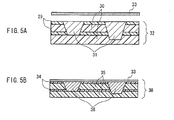
- a first layer 39 and a release film 41 provided with a second layer 40 are prepared (FIG. 6A).
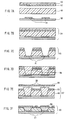
- FIGS. 7A to 7F are schematic cross-sectional views showing an example of a method for manufacturing a circuit board of the present invention and correspond to individual steps in the manufacturing method.
Landscapes
- Engineering & Computer Science (AREA)
- Microelectronics & Electronic Packaging (AREA)
- Manufacturing & Machinery (AREA)
- Textile Engineering (AREA)
- Production Of Multi-Layered Print Wiring Board (AREA)
- Laminated Bodies (AREA)
- Reinforced Plastic Materials (AREA)
Applications Claiming Priority (2)
| Application Number | Priority Date | Filing Date | Title |
|---|---|---|---|
| JP2001328274 | 2001-10-25 | ||
| JP2001328274 | 2001-10-25 |
Publications (3)
| Publication Number | Publication Date |
|---|---|
| EP1307075A2 true EP1307075A2 (fr) | 2003-05-02 |
| EP1307075A3 EP1307075A3 (fr) | 2004-12-29 |
| EP1307075B1 EP1307075B1 (fr) | 2007-01-24 |
Family
ID=19144366
Family Applications (1)
| Application Number | Title | Priority Date | Filing Date |
|---|---|---|---|
| EP20020023716 Expired - Lifetime EP1307075B1 (fr) | 2001-10-25 | 2002-10-23 | Pré-imprégné et panneau de circuit et leur procédé de fabrication |
Country Status (5)
| Country | Link |
|---|---|
| US (1) | US7045198B2 (fr) |
| EP (1) | EP1307075B1 (fr) |
| CN (1) | CN1265687C (fr) |
| DE (1) | DE60217793T2 (fr) |
| TW (1) | TW545092B (fr) |
Cited By (1)
| Publication number | Priority date | Publication date | Assignee | Title |
|---|---|---|---|---|
| US7816611B2 (en) * | 2003-01-14 | 2010-10-19 | Panasonic Corporation | Circuit board |
Families Citing this family (28)
| Publication number | Priority date | Publication date | Assignee | Title |
|---|---|---|---|---|
| US20040214006A1 (en) * | 2003-04-25 | 2004-10-28 | Matsushita Electric Industrial Co., Ltd. | Member for a circuit board, method of manufacturing the same, and methods of manufacturing circuit boards |
| JP2005144816A (ja) * | 2003-11-13 | 2005-06-09 | Tomoegawa Paper Co Ltd | フレキシブル金属積層体 |
| JPWO2006118141A1 (ja) * | 2005-04-28 | 2008-12-18 | 松下電器産業株式会社 | 多層配線基板およびその製造方法 |
| GB0619539D0 (en) * | 2006-10-04 | 2006-11-15 | Hexcel Composites Ltd | Curable resin films |
| KR100796983B1 (ko) * | 2006-11-21 | 2008-01-22 | 삼성전기주식회사 | 인쇄회로기판 및 그 제조방법 |
| US7537827B1 (en) * | 2006-12-13 | 2009-05-26 | Henkel Corporation | Prepreg laminates |
| GB0703172D0 (en) * | 2007-02-19 | 2007-03-28 | Pa Knowledge Ltd | Printed circuit boards |
| WO2009045932A1 (fr) | 2007-09-28 | 2009-04-09 | Tri-Star Laminates, Inc. | Meilleurs systèmes et procédés de perçage de trous dans des cartes à circuit imprimé |
| KR101591619B1 (ko) | 2008-08-18 | 2016-02-04 | 셈블란트 리미티드 | 할로-하이드로카본 폴리머 코팅 |
| US8383948B2 (en) * | 2009-09-18 | 2013-02-26 | Ibiden Co., Ltd. | Flex-rigid wiring board and method for manufacturing the same |
| JP2011096900A (ja) * | 2009-10-30 | 2011-05-12 | Fujitsu Ltd | 導電体およびプリント配線板並びにそれらの製造方法 |
| US8995146B2 (en) | 2010-02-23 | 2015-03-31 | Semblant Limited | Electrical assembly and method |
| KR20110113980A (ko) * | 2010-04-12 | 2011-10-19 | 삼성전자주식회사 | 필름을 포함한 다층 인쇄회로기판 및 그 제조 방법 |
| JP5528250B2 (ja) | 2010-07-30 | 2014-06-25 | 日東電工株式会社 | 配線回路基板の製造方法 |
| CN102260378B (zh) * | 2011-05-06 | 2013-03-20 | 广东生益科技股份有限公司 | 复合材料、用其制作的高频电路基板及其制作方法 |
| JP5849205B2 (ja) * | 2011-11-22 | 2016-01-27 | パナソニックIpマネジメント株式会社 | 金属張積層板及びプリント配線板 |
| WO2014046014A1 (fr) * | 2012-09-20 | 2014-03-27 | 株式会社クラレ | Carte de circuit imprimé et son procédé de fabrication |
| CN103906360A (zh) * | 2012-12-28 | 2014-07-02 | 富葵精密组件(深圳)有限公司 | 柔性电路板及其制作方法 |
| CN104254213A (zh) * | 2013-06-27 | 2014-12-31 | 宏启胜精密电子(秦皇岛)有限公司 | 多层电路板及其制作方法 |
| US9899330B2 (en) * | 2014-10-03 | 2018-02-20 | Mc10, Inc. | Flexible electronic circuits with embedded integrated circuit die |
| JP2016219452A (ja) * | 2015-05-14 | 2016-12-22 | 富士通株式会社 | 多層基板及び多層基板の製造方法 |
| KR20180068950A (ko) * | 2015-10-07 | 2018-06-22 | 세키스이가가쿠 고교가부시키가이샤 | 접착제층 부착 금속 피복 부직포, 접착제층 부착 금속 피복 부직포의 제조 방법, 및 피복 심선 |
| US10849222B2 (en) * | 2016-11-14 | 2020-11-24 | Pioneer Circuits, Inc. | High temperature resistant fabric and its use in flexible circuits |
| GB201621177D0 (en) | 2016-12-13 | 2017-01-25 | Semblant Ltd | Protective coating |
| GB201709925D0 (en) * | 2017-06-21 | 2017-08-02 | Royal College Of Art | Composite structure |
| TWI725538B (zh) * | 2019-09-04 | 2021-04-21 | 台燿科技股份有限公司 | 金屬箔積層板、印刷電路板、及金屬箔積層板之製法 |
| JP7031955B2 (ja) * | 2019-09-10 | 2022-03-08 | Fict株式会社 | 回路基板の製造方法 |
| JP7437993B2 (ja) * | 2020-03-26 | 2024-02-26 | 日本メクトロン株式会社 | フレキシブルプリント配線板を用いたヒータ及びその製造方法 |
Family Cites Families (13)
| Publication number | Priority date | Publication date | Assignee | Title |
|---|---|---|---|---|
| US4005238A (en) * | 1973-10-25 | 1977-01-25 | Akademie Der Wissenschaften Der Ddr | Metallized articles and method of producing the same |
| JPS6397635A (ja) * | 1986-10-14 | 1988-04-28 | Ube Ind Ltd | インタ−リ−フを有する繊維強化エポキシ樹脂プリプレグ |
| JPH01225539A (ja) * | 1988-03-04 | 1989-09-08 | Junkosha Co Ltd | 積層板 |
| JPH02181997A (ja) * | 1989-01-07 | 1990-07-16 | Fujitsu Ltd | 多層プリント配線板 |
| US5065227A (en) * | 1990-06-04 | 1991-11-12 | International Business Machines Corporation | Integrated circuit packaging using flexible substrate |
| JPH05299796A (ja) * | 1992-04-22 | 1993-11-12 | Hitachi Chem Co Ltd | 多層印刷配線板用接着シートおよびそれを用いた金属張積層板 |
| JP2601128B2 (ja) * | 1992-05-06 | 1997-04-16 | 松下電器産業株式会社 | 回路形成用基板の製造方法および回路形成用基板 |
| DE59309575D1 (de) * | 1992-06-15 | 1999-06-17 | Heinze Dyconex Patente | Verfahren zur herstellung von leiterplatten unter verwendung eines halbzeuges mit extrem dichter verdrahtung für die signalführung |
| JP3197213B2 (ja) * | 1996-05-29 | 2001-08-13 | 松下電器産業株式会社 | プリント配線板およびその製造方法 |
| SG86345A1 (en) * | 1998-05-14 | 2002-02-19 | Matsushita Electric Industrial Co Ltd | Circuit board and method of manufacturing the same |
| JP2002094200A (ja) | 2000-09-18 | 2002-03-29 | Matsushita Electric Ind Co Ltd | 回路基板用電気絶縁材と回路基板およびその製造方法 |
| JP2002176268A (ja) | 2000-09-27 | 2002-06-21 | Matsushita Electric Ind Co Ltd | 樹脂基板、樹脂基板の製造方法、接続中間体、回路基板、および回路基板の製造方法 |
| EP1194020A3 (fr) | 2000-09-27 | 2004-03-31 | Matsushita Electric Industrial Co., Ltd. | Panneau de résine, procédé de fabrication d'une panneau de résine, corps à interconnexions, panneau à circuit et procédé de fabrication d'un panneau à circuit |
-
2002
- 2002-10-17 TW TW091123901A patent/TW545092B/zh not_active IP Right Cessation
- 2002-10-23 EP EP20020023716 patent/EP1307075B1/fr not_active Expired - Lifetime
- 2002-10-23 DE DE2002617793 patent/DE60217793T2/de not_active Expired - Fee Related
- 2002-10-24 US US10/280,762 patent/US7045198B2/en not_active Expired - Fee Related
- 2002-10-25 CN CNB02147043XA patent/CN1265687C/zh not_active Expired - Fee Related
Cited By (1)
| Publication number | Priority date | Publication date | Assignee | Title |
|---|---|---|---|---|
| US7816611B2 (en) * | 2003-01-14 | 2010-10-19 | Panasonic Corporation | Circuit board |
Also Published As
| Publication number | Publication date |
|---|---|
| TW545092B (en) | 2003-08-01 |
| CN1265687C (zh) | 2006-07-19 |
| CN1414822A (zh) | 2003-04-30 |
| EP1307075A3 (fr) | 2004-12-29 |
| EP1307075B1 (fr) | 2007-01-24 |
| US20030082363A1 (en) | 2003-05-01 |
| DE60217793D1 (de) | 2007-03-15 |
| US7045198B2 (en) | 2006-05-16 |
| DE60217793T2 (de) | 2007-10-18 |
Similar Documents
| Publication | Publication Date | Title |
|---|---|---|
| EP1307075B1 (fr) | Pré-imprégné et panneau de circuit et leur procédé de fabrication | |
| US6734375B2 (en) | Circuit board having an interstitial inner via hole structure | |
| US7103971B2 (en) | Process for manufacturing a circuit board | |
| JP2587596B2 (ja) | 回路基板接続材とそれを用いた多層回路基板の製造方法 | |
| US6753483B2 (en) | Printed circuit board and method of manufacturing the same | |
| JP3197213B2 (ja) | プリント配線板およびその製造方法 | |
| US20020038725A1 (en) | Circuit board and production of the same | |
| US8198551B2 (en) | Power core for use in circuitized substrate and method of making same | |
| EP3646369A1 (fr) | Carte de circuit imprimé multicouche utilisant une couche d'interposeur et une pâte conductrice | |
| JP2007266606A (ja) | 回路基板用のフルオロポリマー絶縁性組成物およびこれから成る回路基板 | |
| US20040170795A1 (en) | Lasable bond-ply materials for high density printed wiring boards | |
| US7145221B2 (en) | Low moisture absorptive circuitized substrate, method of making same, electrical assembly utilizing same, and information handling system utilizing same | |
| JP3441945B2 (ja) | プリント配線板およびその製造方法 | |
| EP1404165A1 (fr) | Procede de fabrication de panneaux de cablage multicouche | |
| JP3138215B2 (ja) | 回路基板用基材とプリプレグ及びそれを用いたプリント回路基板 | |
| JP2003200535A (ja) | プリプレグおよび回路基板、ならびにそれらの製造方法 | |
| JPH08316598A (ja) | プリント配線板およびその製造方法 | |
| JP3153511B2 (ja) | プリント配線板およびその製造方法 | |
| JP3728059B2 (ja) | 多層配線基板 | |
| KR101281898B1 (ko) | 다층 프린트배선판 및 그 제조방법 | |
| JP2002176268A (ja) | 樹脂基板、樹脂基板の製造方法、接続中間体、回路基板、および回路基板の製造方法 | |
| JP2004082554A (ja) | 絶縁フィルムおよびこれを用いた多層配線基板 | |
| JP2003218160A (ja) | 絶縁フィルムおよびこれを用いた多層配線基板 | |
| JP2004090238A (ja) | 絶縁フィルムおよびこれを用いた多層配線基板 | |
| JP2005136051A (ja) | 配線基板の製造方法 |
Legal Events
| Date | Code | Title | Description |
|---|---|---|---|
| PUAI | Public reference made under article 153(3) epc to a published international application that has entered the european phase |
Free format text: ORIGINAL CODE: 0009012 |
|
| AK | Designated contracting states |
Designated state(s): AT BE BG CH CY CZ DE DK EE ES FI FR GB GR IE IT LI LU MC NL PT SE SK TR |
|
| AX | Request for extension of the european patent |
Extension state: AL LT LV MK RO SI |
|
| RIN1 | Information on inventor provided before grant (corrected) |
Inventor name: ECHIGO, FUMIO Inventor name: SUZUKI, TAKESHI Inventor name: NAKAGIRI, YASUSHI |
|
| PUAL | Search report despatched |
Free format text: ORIGINAL CODE: 0009013 |
|
| AK | Designated contracting states |
Kind code of ref document: A3 Designated state(s): AT BE BG CH CY CZ DE DK EE ES FI FR GB GR IE IT LI LU MC NL PT SE SK TR |
|
| AX | Request for extension of the european patent |
Extension state: AL LT LV MK RO SI |
|
| 17P | Request for examination filed |
Effective date: 20050224 |
|
| AKX | Designation fees paid |
Designated state(s): DE FR GB |
|
| GRAP | Despatch of communication of intention to grant a patent |
Free format text: ORIGINAL CODE: EPIDOSNIGR1 |
|
| GRAS | Grant fee paid |
Free format text: ORIGINAL CODE: EPIDOSNIGR3 |
|
| GRAA | (expected) grant |
Free format text: ORIGINAL CODE: 0009210 |
|
| AK | Designated contracting states |
Kind code of ref document: B1 Designated state(s): DE FR GB |
|
| REG | Reference to a national code |
Ref country code: GB Ref legal event code: FG4D |
|
| RIN1 | Information on inventor provided before grant (corrected) |
Inventor name: ECHIGO, FUMIO Inventor name: SUZUKI, TAKESHI Inventor name: NAKAGIRI, YASUSHI |
|
| REF | Corresponds to: |
Ref document number: 60217793 Country of ref document: DE Date of ref document: 20070315 Kind code of ref document: P |
|
| ET | Fr: translation filed | ||
| PLBE | No opposition filed within time limit |
Free format text: ORIGINAL CODE: 0009261 |
|
| STAA | Information on the status of an ep patent application or granted ep patent |
Free format text: STATUS: NO OPPOSITION FILED WITHIN TIME LIMIT |
|
| 26N | No opposition filed |
Effective date: 20071025 |
|
| PGFP | Annual fee paid to national office [announced via postgrant information from national office to epo] |
Ref country code: DE Payment date: 20081016 Year of fee payment: 7 |
|
| PGFP | Annual fee paid to national office [announced via postgrant information from national office to epo] |
Ref country code: GB Payment date: 20081022 Year of fee payment: 7 |
|
| PGFP | Annual fee paid to national office [announced via postgrant information from national office to epo] |
Ref country code: FR Payment date: 20091029 Year of fee payment: 8 |
|
| PG25 | Lapsed in a contracting state [announced via postgrant information from national office to epo] |
Ref country code: DE Free format text: LAPSE BECAUSE OF NON-PAYMENT OF DUE FEES Effective date: 20100501 |
|
| PG25 | Lapsed in a contracting state [announced via postgrant information from national office to epo] |
Ref country code: GB Free format text: LAPSE BECAUSE OF NON-PAYMENT OF DUE FEES Effective date: 20091023 |
|
| PG25 | Lapsed in a contracting state [announced via postgrant information from national office to epo] |
Ref country code: FR Free format text: LAPSE BECAUSE OF NON-PAYMENT OF DUE FEES Effective date: 20101102 |
|
| REG | Reference to a national code |
Ref country code: FR Ref legal event code: ST Effective date: 20110630 |