EP1309089A1 - Commutateur de puissance pour la commande du moteur d'une commande d'aiguillage - Google Patents
Commutateur de puissance pour la commande du moteur d'une commande d'aiguillage Download PDFInfo
- Publication number
- EP1309089A1 EP1309089A1 EP01440351A EP01440351A EP1309089A1 EP 1309089 A1 EP1309089 A1 EP 1309089A1 EP 01440351 A EP01440351 A EP 01440351A EP 01440351 A EP01440351 A EP 01440351A EP 1309089 A1 EP1309089 A1 EP 1309089A1
- Authority
- EP
- European Patent Office
- Prior art keywords
- diode
- transistor
- circuit breaker
- transistors
- anode
- Prior art date
- Legal status (The legal status is an assumption and is not a legal conclusion. Google has not performed a legal analysis and makes no representation as to the accuracy of the status listed.)
- Granted
Links
- 230000005669 field effect Effects 0.000 claims description 12
- 239000004065 semiconductor Substances 0.000 claims description 7
- 230000006378 damage Effects 0.000 description 2
- 230000006698 induction Effects 0.000 description 2
- 238000002955 isolation Methods 0.000 description 2
- 238000004804 winding Methods 0.000 description 2
- 230000001419 dependent effect Effects 0.000 description 1
- 230000001939 inductive effect Effects 0.000 description 1
Images
Classifications
-
- H—ELECTRICITY
- H03—ELECTRONIC CIRCUITRY
- H03K—PULSE TECHNIQUE
- H03K17/00—Electronic switching or gating, i.e. not by contact-making and –breaking
- H03K17/08—Modifications for protecting switching circuit against overcurrent or overvoltage
- H03K17/082—Modifications for protecting switching circuit against overcurrent or overvoltage by feedback from the output to the control circuit
- H03K17/0822—Modifications for protecting switching circuit against overcurrent or overvoltage by feedback from the output to the control circuit in field-effect transistor switches
-
- B—PERFORMING OPERATIONS; TRANSPORTING
- B61—RAILWAYS
- B61L—GUIDING RAILWAY TRAFFIC; ENSURING THE SAFETY OF RAILWAY TRAFFIC
- B61L7/00—Remote control of local operating means for points, signals, or track-mounted scotch-blocks
- B61L7/06—Remote control of local operating means for points, signals, or track-mounted scotch-blocks using electrical transmission
- B61L7/068—Protection against eddy-currents, short-circuits, or the like, for electric safety arrangements
-
- H—ELECTRICITY
- H03—ELECTRONIC CIRCUITRY
- H03K—PULSE TECHNIQUE
- H03K17/00—Electronic switching or gating, i.e. not by contact-making and –breaking
- H03K17/51—Electronic switching or gating, i.e. not by contact-making and –breaking characterised by the components used
- H03K17/56—Electronic switching or gating, i.e. not by contact-making and –breaking characterised by the components used by the use, as active elements, of semiconductor devices
- H03K17/687—Electronic switching or gating, i.e. not by contact-making and –breaking characterised by the components used by the use, as active elements, of semiconductor devices the devices being field-effect transistors
- H03K17/6871—Electronic switching or gating, i.e. not by contact-making and –breaking characterised by the components used by the use, as active elements, of semiconductor devices the devices being field-effect transistors the output circuit comprising more than one controlled field-effect transistor
- H03K17/6874—Electronic switching or gating, i.e. not by contact-making and –breaking characterised by the components used by the use, as active elements, of semiconductor devices the devices being field-effect transistors the output circuit comprising more than one controlled field-effect transistor in a symmetrical configuration
-
- H—ELECTRICITY
- H03—ELECTRONIC CIRCUITRY
- H03K—PULSE TECHNIQUE
- H03K17/00—Electronic switching or gating, i.e. not by contact-making and –breaking
- H03K17/51—Electronic switching or gating, i.e. not by contact-making and –breaking characterised by the components used
- H03K17/56—Electronic switching or gating, i.e. not by contact-making and –breaking characterised by the components used by the use, as active elements, of semiconductor devices
- H03K17/687—Electronic switching or gating, i.e. not by contact-making and –breaking characterised by the components used by the use, as active elements, of semiconductor devices the devices being field-effect transistors
- H03K17/689—Electronic switching or gating, i.e. not by contact-making and –breaking characterised by the components used by the use, as active elements, of semiconductor devices the devices being field-effect transistors with galvanic isolation between the control circuit and the output circuit
- H03K17/691—Electronic switching or gating, i.e. not by contact-making and –breaking characterised by the components used by the use, as active elements, of semiconductor devices the devices being field-effect transistors with galvanic isolation between the control circuit and the output circuit using transformer coupling
-
- H—ELECTRICITY
- H03—ELECTRONIC CIRCUITRY
- H03K—PULSE TECHNIQUE
- H03K17/00—Electronic switching or gating, i.e. not by contact-making and –breaking
- H03K17/51—Electronic switching or gating, i.e. not by contact-making and –breaking characterised by the components used
- H03K17/78—Electronic switching or gating, i.e. not by contact-making and –breaking characterised by the components used using opto-electronic devices, i.e. light-emitting and photoelectric devices electrically- or optically-coupled
- H03K17/795—Electronic switching or gating, i.e. not by contact-making and –breaking characterised by the components used using opto-electronic devices, i.e. light-emitting and photoelectric devices electrically- or optically-coupled controlling bipolar transistors
- H03K17/7955—Electronic switching or gating, i.e. not by contact-making and –breaking characterised by the components used using opto-electronic devices, i.e. light-emitting and photoelectric devices electrically- or optically-coupled controlling bipolar transistors using phototransistors
-
- H—ELECTRICITY
- H03—ELECTRONIC CIRCUITRY
- H03K—PULSE TECHNIQUE
- H03K17/00—Electronic switching or gating, i.e. not by contact-making and –breaking
- H03K17/51—Electronic switching or gating, i.e. not by contact-making and –breaking characterised by the components used
- H03K17/78—Electronic switching or gating, i.e. not by contact-making and –breaking characterised by the components used using opto-electronic devices, i.e. light-emitting and photoelectric devices electrically- or optically-coupled
- H03K17/785—Electronic switching or gating, i.e. not by contact-making and –breaking characterised by the components used using opto-electronic devices, i.e. light-emitting and photoelectric devices electrically- or optically-coupled controlling field-effect transistor switches
Definitions
- the invention relates to a circuit breaker, in particular for control purposes the motor of a point machine.
- the motor in the railway switch machine is usually a 400 volt Three-phase asynchronous motor. A high starting current is required when switching on switch, high induction voltages arise when switching off. This Stress leads to wear on the relays used Contacts.
- the object of the invention is a wear-free, reliable switch to accomplish.
- Semiconductors are used for wear-free switching of loads. This are very sensitive to short circuits and usually become very often destroyed. Since the rate of increase in the supply network Short-circuit current through inductive components is limited, however the circuit breaker can be quickly switched off in the event of a short circuit, causing destruction is avoided.
- the semiconductor circuit breaker is used to control the switch motor used. It switches off short-circuit currents without destruction. So achieved the semiconductor switch is more reliable than a relay.
- a fuse is no longer used to protect a short circuit required, consequently it can no longer melt.
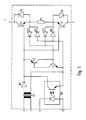
- FIG. 1 shows a schematic representation of a Circuit breaker.
- the circuit breaker is used in particular to control the motor Point machine used, but can also be used for controls any motor or generator can be used.
- the circuit breaker is used to switch an alternating voltage between points 1 and 2. There are at least two for switching three-phase current such circuit breakers required.
- Diode D5 is connected in parallel with transistor T1, in parallel with transistor T2 diode D6.
- the circuit breaker is switched on via points 3 and 4 and via points 5 and 6 switched off.
- Points 3 and 4 are with the Primary winding of a transformer U1 connected.
- Points 5 and 6 are with connected to the inputs of an opto-coupler D8.
- the secondary winding of the transformer U1 is on the one hand via diode D7 one output of the opto-coupler D8 and the control inputs of the Transistors T1 and T2 and the other with the other output of the Opto-coupler D8 connected.
- Transistor T3 is a pnp transistor, transistor T4 a npn transistor.
- the emitter of transistor T3 is connected to the control inputs the transistors T1 and T2 connected, the collector to the Control input of transistor T4.
- the collector of transistor T4 is with connected to the control input of transistor T3, the emitter to the other output of the optocoupler D8.
- a simulated Griger bridge containing diodes D1, D2, D3, D4 provided.
- the anode of diode D1 is with the source connection connected by transistor T1, the cathode to the control input of Transistor T4.
- the anode of diode D2 is connected to the other output of the Opto-coupler D8 connected the cathode to the anode of diode D1.
- the anode of diode D3 is connected to the source of transistor T2 connected, the cathode to the cathode of the diode D1.
- the anode of diode D4 is connected to the anode of diode D2, the cathode to the anode the diode D3.
- the anode of diode D5 is with the anode of diode D1 connected, the cathode to point 1 and the drain of the Transistor T1.
- the anode of diode D6 is with the anode of diode D3 connected, the cathode to point 2 and the drain of the Transistor T2.
- the transistors T1 and T2 each switch a half-wave AC voltage.
- a quick shutdown is done by applying a DC voltage to the Points 5 and 6 achieved.
- the gate-source capacitances are then via opto-couplers D8 of the transistors T1 and T2 quickly discharged.
- Points 5 and 6 thus serve as control inputs for switching off the Circuit breaker.
- the Grayne bridge formed from diodes D1 to D4 ensures that Short-circuit currents of both half-waves lead to shutdown.
Landscapes
- Engineering & Computer Science (AREA)
- Mechanical Engineering (AREA)
- Power Engineering (AREA)
- Control Of Direct Current Motors (AREA)
- Control Of Stepping Motors (AREA)
- Motor And Converter Starters (AREA)
- High-Pressure Fuel Injection Pump Control (AREA)
Priority Applications (3)
| Application Number | Priority Date | Filing Date | Title |
|---|---|---|---|
| EP01440351A EP1309089B1 (fr) | 2001-10-22 | 2001-10-22 | Commutateur de puissance pour la commande du moteur d'une commande d'aiguillage |
| DE50112646T DE50112646D1 (de) | 2001-10-22 | 2001-10-22 | Leistungsschalter zur Steuerung des Motors eines Weichenantriebs |
| AT01440351T ATE365395T1 (de) | 2001-10-22 | 2001-10-22 | Leistungsschalter zur steuerung des motors eines weichenantriebs |
Applications Claiming Priority (1)
| Application Number | Priority Date | Filing Date | Title |
|---|---|---|---|
| EP01440351A EP1309089B1 (fr) | 2001-10-22 | 2001-10-22 | Commutateur de puissance pour la commande du moteur d'une commande d'aiguillage |
Publications (2)
| Publication Number | Publication Date |
|---|---|
| EP1309089A1 true EP1309089A1 (fr) | 2003-05-07 |
| EP1309089B1 EP1309089B1 (fr) | 2007-06-20 |
Family
ID=8183324
Family Applications (1)
| Application Number | Title | Priority Date | Filing Date |
|---|---|---|---|
| EP01440351A Expired - Lifetime EP1309089B1 (fr) | 2001-10-22 | 2001-10-22 | Commutateur de puissance pour la commande du moteur d'une commande d'aiguillage |
Country Status (3)
| Country | Link |
|---|---|
| EP (1) | EP1309089B1 (fr) |
| AT (1) | ATE365395T1 (fr) |
| DE (1) | DE50112646D1 (fr) |
Cited By (3)
| Publication number | Priority date | Publication date | Assignee | Title |
|---|---|---|---|---|
| WO2006047971A1 (fr) * | 2004-11-02 | 2006-05-11 | Azd Praha S.R.O. | Commutateur sans contact triphase sur |
| WO2011107376A1 (fr) * | 2010-03-05 | 2011-09-09 | Siemens Aktiengesellschaft | Installation de circuit pour la mesure de tension dans une commande électrique, en particulier une commande d'aiguillage |
| WO2025261981A1 (fr) * | 2024-06-21 | 2025-12-26 | BSH Hausgeräte GmbH | Dispositif électrique, appareil électrique et procédé de fonctionnement d'un dispositif électrique |
Citations (4)
| Publication number | Priority date | Publication date | Assignee | Title |
|---|---|---|---|---|
| DE3445340A1 (de) * | 1984-12-12 | 1986-06-19 | Staiber, Heinrich, 8201 Bad Feilnbach | Mosfet - zweirichtungsschalter mit strombegrenzung |
| DE3723786A1 (de) * | 1987-07-16 | 1989-01-26 | Licentia Gmbh | Anordnung zur selbsttaetigen ueberstromabschaltung |
| JPH11225055A (ja) * | 1998-02-09 | 1999-08-17 | Sharp Corp | 光結合装置 |
| US5999387A (en) * | 1993-09-08 | 1999-12-07 | Siemens Aktiengesellschaft | Current limiting device |
-
2001
- 2001-10-22 EP EP01440351A patent/EP1309089B1/fr not_active Expired - Lifetime
- 2001-10-22 DE DE50112646T patent/DE50112646D1/de not_active Expired - Lifetime
- 2001-10-22 AT AT01440351T patent/ATE365395T1/de not_active IP Right Cessation
Patent Citations (4)
| Publication number | Priority date | Publication date | Assignee | Title |
|---|---|---|---|---|
| DE3445340A1 (de) * | 1984-12-12 | 1986-06-19 | Staiber, Heinrich, 8201 Bad Feilnbach | Mosfet - zweirichtungsschalter mit strombegrenzung |
| DE3723786A1 (de) * | 1987-07-16 | 1989-01-26 | Licentia Gmbh | Anordnung zur selbsttaetigen ueberstromabschaltung |
| US5999387A (en) * | 1993-09-08 | 1999-12-07 | Siemens Aktiengesellschaft | Current limiting device |
| JPH11225055A (ja) * | 1998-02-09 | 1999-08-17 | Sharp Corp | 光結合装置 |
Non-Patent Citations (1)
| Title |
|---|
| PATENT ABSTRACTS OF JAPAN vol. 1999, no. 13 30 November 1999 (1999-11-30) * |
Cited By (3)
| Publication number | Priority date | Publication date | Assignee | Title |
|---|---|---|---|---|
| WO2006047971A1 (fr) * | 2004-11-02 | 2006-05-11 | Azd Praha S.R.O. | Commutateur sans contact triphase sur |
| WO2011107376A1 (fr) * | 2010-03-05 | 2011-09-09 | Siemens Aktiengesellschaft | Installation de circuit pour la mesure de tension dans une commande électrique, en particulier une commande d'aiguillage |
| WO2025261981A1 (fr) * | 2024-06-21 | 2025-12-26 | BSH Hausgeräte GmbH | Dispositif électrique, appareil électrique et procédé de fonctionnement d'un dispositif électrique |
Also Published As
| Publication number | Publication date |
|---|---|
| DE50112646D1 (de) | 2007-08-02 |
| ATE365395T1 (de) | 2007-07-15 |
| EP1309089B1 (fr) | 2007-06-20 |
Similar Documents
| Publication | Publication Date | Title |
|---|---|---|
| DE102016224706B4 (de) | Gate-Antriebsschaltung für Halbleiterschaltgeräte | |
| DE10020981B4 (de) | Motor-Steuergerät mit Fehlerschutzschaltung | |
| DE10063084B4 (de) | Leistungselektronische Schaltung | |
| DE69122419T2 (de) | Schutzschaltung für eine Halbleiteranordnung | |
| EP0148855B1 (fr) | Circuit de commutation de puissance a mosfet en parallele | |
| DE102007009885A1 (de) | Halbleiterschaltung | |
| DE102008055157A1 (de) | Ansteuerschaltung für eine Leistungshalbleiteranordnung und Leistungshalbleiteranordnung | |
| EP0717886B1 (fr) | Limiteur de courant | |
| DE3622293A1 (de) | Festkoerper-nebenschlussschaltkreis fuer leckstromleistungssteuerung | |
| EP1783910B1 (fr) | Circuit et un procédé pour commander d'une manière galvaniquement séparée un commutateur semi-conducteur | |
| DE4428675A1 (de) | Schaltungsanordnung zum Schutz eines abschaltbaren Leistungshalbleiter-Schalters vor Überspannungen | |
| WO2009077369A1 (fr) | Générateur avec montage redresseur | |
| DE102013106801B4 (de) | Leistungshalbleiterschaltung | |
| DE19648562C2 (de) | Verfahren und Vorrichtung zur Stromüberwachung für Halbleiterschaltungen | |
| EP1923986B1 (fr) | Contrôleur de courant alternatif pour des commutateur électromagnétique | |
| EP1309089B1 (fr) | Commutateur de puissance pour la commande du moteur d'une commande d'aiguillage | |
| WO2002023704A1 (fr) | Circuit d'alimentation en energie destine a un circuit de commande d'un commutateur a semi-conducteur de puissance et procede pour mettre l'energie de commande a disposition d'un commutateur a semi-conducteur de puissance | |
| DE10156963A1 (de) | Schaltungsanordnung zum zuverlässigen Schalten von Stromkreisen | |
| DE4037348C1 (en) | Protective circuitry for power semiconductor switches - uses bridging voltage clamping circuit consisting of diode and Zener diode belonging to rectifier pair | |
| EP1564618B1 (fr) | Circuit pour la correction du facteur de puissance dans alimentations de puissance à découpage, chargeurs et similaires. | |
| EP0590167B1 (fr) | Commutateurs de puissance avec inductance de limitation de courant | |
| DE3321838C2 (fr) | ||
| DE102005045552B4 (de) | Schaltungsanordnung | |
| EP1608208B1 (fr) | Circuit avec dispositif de coupure pour alimenter des sources lumineuses | |
| DE3229426C2 (de) | Reihenschaltung zweier Leistungs-Halbleiterschalter |
Legal Events
| Date | Code | Title | Description |
|---|---|---|---|
| PUAI | Public reference made under article 153(3) epc to a published international application that has entered the european phase |
Free format text: ORIGINAL CODE: 0009012 |
|
| 17P | Request for examination filed |
Effective date: 20020726 |
|
| AK | Designated contracting states |
Designated state(s): AT BE CH CY DE DK ES FI FR GB GR IE IT LI LU MC NL PT SE TR |
|
| AX | Request for extension of the european patent |
Extension state: AL LT LV MK RO SI |
|
| AKX | Designation fees paid |
Designated state(s): AT BE CH CY DE DK ES FI FR GB GR IE IT LI LU MC NL PT SE TR |
|
| GRAP | Despatch of communication of intention to grant a patent |
Free format text: ORIGINAL CODE: EPIDOSNIGR1 |
|
| RAP1 | Party data changed (applicant data changed or rights of an application transferred) |
Owner name: ALCATEL LUCENT |
|
| GRAS | Grant fee paid |
Free format text: ORIGINAL CODE: EPIDOSNIGR3 |
|
| GRAA | (expected) grant |
Free format text: ORIGINAL CODE: 0009210 |
|
| RAP1 | Party data changed (applicant data changed or rights of an application transferred) |
Owner name: ALCATEL TRANSPORT SOLUTIONS HOLDING GMBH |
|
| AK | Designated contracting states |
Kind code of ref document: B1 Designated state(s): AT BE CH CY DE DK ES FI FR GB GR IE IT LI LU MC NL PT SE TR |
|
| REG | Reference to a national code |
Ref country code: GB Ref legal event code: FG4D Free format text: NOT ENGLISH |
|
| REG | Reference to a national code |
Ref country code: CH Ref legal event code: EP |
|
| REG | Reference to a national code |
Ref country code: IE Ref legal event code: FG4D Free format text: LANGUAGE OF EP DOCUMENT: GERMAN |
|
| GBT | Gb: translation of ep patent filed (gb section 77(6)(a)/1977) |
Effective date: 20070710 |
|
| REF | Corresponds to: |
Ref document number: 50112646 Country of ref document: DE Date of ref document: 20070802 Kind code of ref document: P |
|
| PG25 | Lapsed in a contracting state [announced via postgrant information from national office to epo] |
Ref country code: SE Free format text: LAPSE BECAUSE OF FAILURE TO SUBMIT A TRANSLATION OF THE DESCRIPTION OR TO PAY THE FEE WITHIN THE PRESCRIBED TIME-LIMIT Effective date: 20070920 |
|
| NLV1 | Nl: lapsed or annulled due to failure to fulfill the requirements of art. 29p and 29m of the patents act | ||
| ET | Fr: translation filed | ||
| REG | Reference to a national code |
Ref country code: IE Ref legal event code: FD4D |
|
| PG25 | Lapsed in a contracting state [announced via postgrant information from national office to epo] |
Ref country code: ES Free format text: LAPSE BECAUSE OF FAILURE TO SUBMIT A TRANSLATION OF THE DESCRIPTION OR TO PAY THE FEE WITHIN THE PRESCRIBED TIME-LIMIT Effective date: 20071001 Ref country code: NL Free format text: LAPSE BECAUSE OF FAILURE TO SUBMIT A TRANSLATION OF THE DESCRIPTION OR TO PAY THE FEE WITHIN THE PRESCRIBED TIME-LIMIT Effective date: 20070620 Ref country code: PT Free format text: LAPSE BECAUSE OF FAILURE TO SUBMIT A TRANSLATION OF THE DESCRIPTION OR TO PAY THE FEE WITHIN THE PRESCRIBED TIME-LIMIT Effective date: 20071120 Ref country code: IE Free format text: LAPSE BECAUSE OF FAILURE TO SUBMIT A TRANSLATION OF THE DESCRIPTION OR TO PAY THE FEE WITHIN THE PRESCRIBED TIME-LIMIT Effective date: 20070620 |
|
| RAP2 | Party data changed (patent owner data changed or rights of a patent transferred) |
Owner name: THALES SECURITY SOLUTIONS & SERVICES GMBH |
|
| PLBE | No opposition filed within time limit |
Free format text: ORIGINAL CODE: 0009261 |
|
| STAA | Information on the status of an ep patent application or granted ep patent |
Free format text: STATUS: NO OPPOSITION FILED WITHIN TIME LIMIT |
|
| BERE | Be: lapsed |
Owner name: ALCATEL TRANSPORT SOLUTIONS HOLDING G.M.B.H. Effective date: 20071031 |
|
| PG25 | Lapsed in a contracting state [announced via postgrant information from national office to epo] |
Ref country code: DK Free format text: LAPSE BECAUSE OF FAILURE TO SUBMIT A TRANSLATION OF THE DESCRIPTION OR TO PAY THE FEE WITHIN THE PRESCRIBED TIME-LIMIT Effective date: 20070620 Ref country code: GR Free format text: LAPSE BECAUSE OF FAILURE TO SUBMIT A TRANSLATION OF THE DESCRIPTION OR TO PAY THE FEE WITHIN THE PRESCRIBED TIME-LIMIT Effective date: 20070921 |
|
| 26N | No opposition filed |
Effective date: 20080325 |
|
| PG25 | Lapsed in a contracting state [announced via postgrant information from national office to epo] |
Ref country code: MC Free format text: LAPSE BECAUSE OF NON-PAYMENT OF DUE FEES Effective date: 20071031 |
|
| REG | Reference to a national code |
Ref country code: CH Ref legal event code: PL |
|
| REG | Reference to a national code |
Ref country code: FR Ref legal event code: CD |
|
| PG25 | Lapsed in a contracting state [announced via postgrant information from national office to epo] |
Ref country code: LI Free format text: LAPSE BECAUSE OF NON-PAYMENT OF DUE FEES Effective date: 20071031 Ref country code: CH Free format text: LAPSE BECAUSE OF NON-PAYMENT OF DUE FEES Effective date: 20071031 |
|
| PG25 | Lapsed in a contracting state [announced via postgrant information from national office to epo] |
Ref country code: BE Free format text: LAPSE BECAUSE OF NON-PAYMENT OF DUE FEES Effective date: 20071031 |
|
| PG25 | Lapsed in a contracting state [announced via postgrant information from national office to epo] |
Ref country code: AT Free format text: LAPSE BECAUSE OF NON-PAYMENT OF DUE FEES Effective date: 20071022 Ref country code: FI Free format text: LAPSE BECAUSE OF FAILURE TO SUBMIT A TRANSLATION OF THE DESCRIPTION OR TO PAY THE FEE WITHIN THE PRESCRIBED TIME-LIMIT Effective date: 20070620 |
|
| PG25 | Lapsed in a contracting state [announced via postgrant information from national office to epo] |
Ref country code: CY Free format text: LAPSE BECAUSE OF FAILURE TO SUBMIT A TRANSLATION OF THE DESCRIPTION OR TO PAY THE FEE WITHIN THE PRESCRIBED TIME-LIMIT Effective date: 20070620 |
|
| PG25 | Lapsed in a contracting state [announced via postgrant information from national office to epo] |
Ref country code: LU Free format text: LAPSE BECAUSE OF NON-PAYMENT OF DUE FEES Effective date: 20071022 |
|
| PG25 | Lapsed in a contracting state [announced via postgrant information from national office to epo] |
Ref country code: TR Free format text: LAPSE BECAUSE OF FAILURE TO SUBMIT A TRANSLATION OF THE DESCRIPTION OR TO PAY THE FEE WITHIN THE PRESCRIBED TIME-LIMIT Effective date: 20070620 |
|
| REG | Reference to a national code |
Ref country code: FR Ref legal event code: PLFP Year of fee payment: 15 |
|
| REG | Reference to a national code |
Ref country code: FR Ref legal event code: PLFP Year of fee payment: 16 |
|
| REG | Reference to a national code |
Ref country code: FR Ref legal event code: PLFP Year of fee payment: 17 |
|
| REG | Reference to a national code |
Ref country code: FR Ref legal event code: PLFP Year of fee payment: 18 |
|
| PGFP | Annual fee paid to national office [announced via postgrant information from national office to epo] |
Ref country code: IT Payment date: 20201027 Year of fee payment: 20 Ref country code: DE Payment date: 20201028 Year of fee payment: 20 Ref country code: GB Payment date: 20201028 Year of fee payment: 20 Ref country code: FR Payment date: 20201023 Year of fee payment: 20 |
|
| REG | Reference to a national code |
Ref country code: DE Ref legal event code: R071 Ref document number: 50112646 Country of ref document: DE |
|
| REG | Reference to a national code |
Ref country code: GB Ref legal event code: PE20 Expiry date: 20211021 |
|
| PG25 | Lapsed in a contracting state [announced via postgrant information from national office to epo] |
Ref country code: GB Free format text: LAPSE BECAUSE OF EXPIRATION OF PROTECTION Effective date: 20211021 |