EP1608208B1 - Circuit avec dispositif de coupure pour alimenter des sources lumineuses - Google Patents
Circuit avec dispositif de coupure pour alimenter des sources lumineuses Download PDFInfo
- Publication number
- EP1608208B1 EP1608208B1 EP05010914A EP05010914A EP1608208B1 EP 1608208 B1 EP1608208 B1 EP 1608208B1 EP 05010914 A EP05010914 A EP 05010914A EP 05010914 A EP05010914 A EP 05010914A EP 1608208 B1 EP1608208 B1 EP 1608208B1
- Authority
- EP
- European Patent Office
- Prior art keywords
- switch
- circuit
- stage
- joined
- node
- Prior art date
- Legal status (The legal status is an assumption and is not a legal conclusion. Google has not performed a legal analysis and makes no representation as to the accuracy of the status listed.)
- Expired - Lifetime
Links
Images

Classifications
-
- H—ELECTRICITY
- H05—ELECTRIC TECHNIQUES NOT OTHERWISE PROVIDED FOR
- H05B—ELECTRIC HEATING; ELECTRIC LIGHT SOURCES NOT OTHERWISE PROVIDED FOR; CIRCUIT ARRANGEMENTS FOR ELECTRIC LIGHT SOURCES, IN GENERAL
- H05B41/00—Circuit arrangements or apparatus for igniting or operating discharge lamps
- H05B41/14—Circuit arrangements
- H05B41/26—Circuit arrangements in which the lamp is fed by power derived from DC by means of a converter, e.g. by high-voltage DC
- H05B41/28—Circuit arrangements in which the lamp is fed by power derived from DC by means of a converter, e.g. by high-voltage DC using static converters
- H05B41/282—Circuit arrangements in which the lamp is fed by power derived from DC by means of a converter, e.g. by high-voltage DC using static converters with semiconductor devices
- H05B41/285—Arrangements for protecting lamps or circuits against abnormal operating conditions
- H05B41/2851—Arrangements for protecting lamps or circuits against abnormal operating conditions for protecting the circuit against abnormal operating conditions
- H05B41/2856—Arrangements for protecting lamps or circuits against abnormal operating conditions for protecting the circuit against abnormal operating conditions against internal abnormal circuit conditions
-
- Y—GENERAL TAGGING OF NEW TECHNOLOGICAL DEVELOPMENTS; GENERAL TAGGING OF CROSS-SECTIONAL TECHNOLOGIES SPANNING OVER SEVERAL SECTIONS OF THE IPC; TECHNICAL SUBJECTS COVERED BY FORMER USPC CROSS-REFERENCE ART COLLECTIONS [XRACs] AND DIGESTS
- Y02—TECHNOLOGIES OR APPLICATIONS FOR MITIGATION OR ADAPTATION AGAINST CLIMATE CHANGE
- Y02B—CLIMATE CHANGE MITIGATION TECHNOLOGIES RELATED TO BUILDINGS, e.g. HOUSING, HOUSE APPLIANCES OR RELATED END-USER APPLICATIONS
- Y02B20/00—Energy efficient lighting technologies, e.g. halogen lamps or gas discharge lamps
Definitions
- the invention relates to a circuit with a shutdown device for the operation of light sources.
- the invention relates to half-bridge inverters for the operation of halogen incandescent lamps.
- Half-wave inverters are well-known for operating light sources.
- the half-bridge inverter is powered by a supply voltage, which is a DC voltage.
- a supply voltage which is a DC voltage.
- the DC voltage can be pulsed without affecting the quality of the light.
- Halogen incandescent lamps represent such a light source.
- Half-bridge inverters for halogen incandescent lamps are therefore generally fed by a rectified mains voltage as a supply voltage, with no smoothing provided.
- half-bridge inverters for halogen incandescent lamps are designed as self-oscillating inverters for cost reasons.
- Self-oscillating in this context means that an output circuit for a drive signal for electronic switch of the half-bridge is removed.
- a half-bridge inverter is always understood as a self-oscillating half-bridge inverter. It consists essentially of the series connection of an upper and a lower electronic switch, which in a half-bridge center are connected and connected between the supply voltage and a ground potential.
- the oscillation of the half-bridge inverter must be started by a starting circuit. This is necessary after each half-wave because the oscillation stops at low instantaneous mains voltage.
- the starting circuit essentially consists of a starting capacitor and a trigger element. As soon as the voltage at the start capacitor exceeds a trigger threshold, a start pulse is triggered; this means that the trigger element switches the starting capacitor to the control electrode of the lower electronic switch. Thus, the lower electronic switch is turned on and the oscillation of the half-bridge inverter starts.
- the starting capacitor has to deliver enough energy to keep the lower electronic switch switched on safely and for a long enough time.
- the circuits in question include a shutdown device.
- the shutdown device has an input and an output. It is designed and switched so that it discharges the starting capacitor if a shutdown signal is present at the input.
- the oscillation of the half-bridge inverter breaks off at the next mains voltage zero crossing. The shutdown prevents a restart.
- the state of the art for a circuit with a shutdown device for the operation of light sources is described below with reference to FIG. 1 explained.
- a terminal for a supply voltage which is marked with a + sign, and a ground potential
- the connection node M forms a half-bridge center.
- the electronic switches are shown as NPN bipolar transistors. However, other electronic switches such. As MOSFET or IGBT can be used. Parallel to each electronic switch in each case an optional freewheeling diode is located.
- the series circuit of two coupling capacitors C7 and C8 is connected.
- a second node N2 is formed.
- the half-bridge inverter which essentially consists of T1, T2, C7 and C8, supplies a high-frequency alternating voltage with respect to a mains voltage.
- the series connection of the primary winding of a feedback transformer Tr1 and a load Lp is connected.
- a coupling capacitor C7 or C8 can be omitted.
- the load is represented by a resistor labeled Lp.
- the load can only consist of one incandescent lamp. However, it is also possible to connect low-voltage halogen incandescent lamps via a transformer.
- the feedback transformer Tr1 detects a load current with the primary winding and couples it via two secondary windings to respective control electrodes of T1 and T2. This closes a feedback loop, creating a self-oscillating half-bridge inverter.
- a start circuit is formed by a start capacitor C3, a resistor R1 and a trigger element DIAC.
- C3 and R1 are connected in series between the supply voltage and the ground potential.
- the DIAC connects the connection point of C3 and R1 to the control electrode of the lower electronic switch T2. Via R1, C3 is charged by the supply voltage.
- C3 gives a start pulse to the control electrode of T2.
- the series connection of a first and a second limiter diode D7 and D8 is connected, wherein the limiter diodes are connected to a third node (N3).
- the third node N3 is connected to the second node N2.
- the limiter diodes are intended to prevent the voltage at the coupling capacitors C7 and C8 from changing polarity when the load current is excessive and thus the potential at the second node N2 does not come to lie above the supply voltage and below the ground potential.
- a shutdown device exists in the prior art FIG. 1 of resistors R3-R6, a capacitor C4, a diode D3 and a transistor T3.
- the voltage at the second node N2 is used.
- the amplitude of the AC component of the voltage at the second node N2 is a measure of the load current. If the load current exceeds a predetermined limit, the circuit should be disabled.
- the voltage at the second node N2 is connected via a fifth capacitor C5 to an input E of the shutdown device.
- the AC component of the voltage at N2 is filtered out by C5 and provided to a ground referenced third resistor R3.
- the voltage at R3 is rectified by a third diode D3 and charges a fourth capacitor C4 via a fourth resistor R4.
- R4 and C4 form a low pass. It serves to ensure that an excessive load current leads to a switch-off process only after a predetermined time. This is necessary because cold filaments of an incandescent lamp, when switched on, in principle lead to an excessive load current. Halogen incandescent lamps typically only reach their nominal value approx. 0.1 sec after switch-on.
- a fifth resistor R5 is connected, which discharges C4 again after an excessive load current.
- the voltage at C4 is supplied to the base of the transistor T3.
- T3 is generally designed as a bipolar transistor. If T3 is activated in the event of a fault, then it short-circuits the starting capacitor C3 via its collector-emitter path. The voltage divider of R6 and R7 adjusts the voltage level at C4 to the switch-on threshold of T3. If necessary, R7 can be omitted.
- FIG. 1 It is shown how a turn-off signal is taken from the node N2 between the coupling capacitors C7 and C8.
- the current in the lower electronic switch T2 serve as a shutdown signal.
- a measuring resistor R2 is connected in series with the lower electronic switch T2. The voltage at R2 is supplied to the input E of the shutdown device. C5 can be omitted.
- a problem with the prior art circuit is the dimensioning of the low pass consisting of R4 and C4.
- the capacitor C4 in the prior art typically has values of 10 to 47 microfarads. These values make C4 large and expensive compared to other circuit components.
- electrolytic capacitors are generally offered for these capacitance values which age, work only in a limited temperature range and are complex in the case of assembly in mass production.
- a circuit which, in addition to the above-described prior art circuit in the turn-off device, comprises a second transistor stage with a collector-connected bipolar transistor. This is the first stage, which is implemented in emitter circuit, downstream.
- transistor stages are known to depend on the transistor electrode associated with both the input of the stage and the output of the stage. In general, this electrode is at ground potential.
- the second stage of the shutdown device according to the invention is in emitter circuit; d. H. the second-stage emitter is connected to the ground potential.
- the emitter circuit is referred to in the literature as voltage follower. It has a high input impedance and a low output impedance. Since the output of the first stage only has to supply low current due to the high input impedance of the second stage, the input of the first stage may have a higher impedance level. This allows the value of C4 in a typical application to be chosen by about one order of magnitude lower.
- the first and second stages include bipolar transistors of different types.
- the first stage includes an NPN transistor and the second stage a PNP transistor. This makes it possible to connect the two stages directly.
- the collector of the first stage can be connected directly to the base of the second stage.
- the second stage of the turn-off device is also used to suppress start pulses in the oscillating half-bridge inverter.
- the base of the transistor of the second stage is coupled to the drive signal of an electronic switch of the half-bridge inverter.
- the electronic switches of the half-bridge inverter are switched on by a positive signal, the following combinations are particularly advantageous: PNP transistor in the second stage coupled with the drive signal of the lower electronic switch; NPN transistor in the second stage coupled with the drive signal of the upper electronic switch.
- the starting capacitor is always discharged when the upper electronic switch turns on.
- the coupling between the drive signal of an electronic switch and the base of the transistor of the second stage via a capacitor compensates potential differences of the coupled circuit points.
- the switching edges of the drive signal are evaluated, resulting in fast switching of the second stage.
- the diode 11 can be turned on in FIG FIG. 1 omitted.
- resistors are denoted by the letter R, transistors by the letter T, diodes by the letter D, nodes by the letter N, and capacitors by the letter C respectively followed by a number. Also, the same reference numerals are used throughout for the same and equivalent elements of the various embodiments.
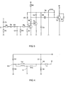
- FIG. 2 is an embodiment of a circuit according to the invention with shutdown device for the operation of light sources shown.
- the turn-off device is extended by the resistor R8 and the transistor T4.
- the collector of the transistor T3 is in contrast to the prior art not directly, but connected via R8 to the starting capacitor C3.
- the collector of T4 is connected to the ground potential. T4 is thus operated in collector circuit.
- the emitter of T4 is connected to the start capacitor C3 and the base of T4 to the collector of T3.
- T3 forms the first stage in the emitter circuit, T4 the second stage in the collector circuit.
- the collector current required by the first stage is reduced.
- the base current of the first stage is reduced, whereby the base circuit of T3 can have a higher impedance level.
- values below 1 microfarad are also possible for the capacitor C4.
- the shutdown signal is fed to the shutdown device at an input E.
- This entrance is also in FIG. 1 and corresponds there also to the input of the cut-off device according to the prior art.
- the rest of the circuit FIG. 1 is in FIG. 2 no longer shown because there are no other differences.
- FIG. 3 is the shutdown device off FIG. 2 extended by a start pulse suppression.
- the base of T4 is connected to the drive signal of the lower electronic switch T2 of the half-bridge inverter via the series connection of a capacitor C6 and a diode D5.
- node N1 is formed at the junction of D5 and C6, node N1 is formed.
- N1 is connected via a parallel connection of a diode D6 and a resistor R9 to the emitter of T4.
- D6 and R9 ensure the charge balance of C6. If R9 is low-impedance enough to provide this charge compensation alone, then D6 can be omitted.
- FIG. 3 connected in series with the diode D3, a Zener diode D4. It allows the cut-off device to be triggered only above a predetermined voltage at input E.
- FIG. 4 a circuit detail is shown which illustrates how a shutdown signal can be generated.
- the coupling capacitors C7, C8 are only charged and discharged to such an extent that the potential at the node N2 moves between the supply voltage + and the ground potential.
- the coupling capacitors C7, C8 are completely discharged or charged with a voltage which is greater than the supply voltage.
- a limiting current flows through the limiter diodes D7, D8.
- the nodes N2 and N3 are directly connected.
- the primary winding of a measuring transformer Tr2 is connected.
- a limiting current can be taken off at a secondary winding of the measuring transformer Tr2 and fed to the input E of the shutdown device. Via a resistor R10, the secondary winding can be provided with a path for a demagnetization current.
- the illustrated possibility of generating a shutdown signal has the advantage that it can sharply distinguish between a normal current and an excessive current and can provide a potential-free shutdown signal.
Landscapes
- Circuit Arrangements For Discharge Lamps (AREA)
- Electronic Switches (AREA)
- Lighting Device Outwards From Vehicle And Optical Signal (AREA)
Claims (4)
- Circuit avec dispositif de coupure pour alimenter des sources lumineuses (Lp), avec les caractéristiques suivantes :• un onduleur à demi-pont auto-oscillant avec un montage en série composé d'un interrupteur électronique supérieur et d'un interrupteur électronique inférieur (T1, T2) qui sont reliés en un point central de demi-pont (M) et qui sont branchés entre une tension d'alimentation (+) et un potentiel de masse,• un condensateur de démarrage (C3) qui est relié par l'intermédiaire d'un élément de déclenchement (DIAC) à une électrode de commande de l'interrupteur électronique inférieur (T2),• un dispositif de coupure avec une entrée (E) et avec une sortie qui est conçu et branché de telle sorte qu'il décharge le condensateur de démarrage (C3) si un signal de coupure se trouve à l'entrée (E),• le dispositif de coupure comprend deux étages de transistors (T3, T4) branchés l'un derrière l'autre et comportant des transistors bipolaires, un premier étage (T3) étant réalisé en émetteur commun et un deuxième étage (T4) étant réalisé en collecteur commun,• le premier étage contient un transistor NPN (T3) et le deuxième étage contient un transistor PNP (T4), l'émetteur du transistor PNP étant relié au condensateur de démarrage (C3),caractérisé par le fait que
la base du transistor du deuxième étage (T4) est couplée de telle sorte au signal de commande de l'interrupteur électronique inférieur (T2) de l'onduleur à demi-pont que, si l'interrupteur électronique inférieur (T2) coupe, le signal de commande de cet interrupteur électronique inférieur (T2) comporte un front descendant qui doit amener le transistor du deuxième étage (T4) à commander. - Circuit avec dispositif de coupure pour alimenter des sources lumineuses (Lp) selon la revendication 1,
caractérisé par les caractéristiques suivantes :• la base du transistor du deuxième étage (T4) est reliée à l'anode d'une cinquième diode (D5),• la cathode de la cinquième diode (D5) est reliée à un premier noeud (N1),• la borne de commande de l'interrupteur électronique inférieur (T2) est reliée par l'intermédiaire d'un sixième condensateur (C6) au premier noeud (N1),• l'émetteur du transistor du deuxième étage (T4) est relié par l'intermédiaire d'une neuvième résistance (R9) au premier noeud (N1). - Circuit avec dispositif de coupure pour alimenter des sources lumineuses (Lp) selon la revendication 1 ou 2,
caractérisé par les caractéristiques suivantes :• le montage en série d'un premier et d'un deuxième condensateur de couplage (C7, C8) est branché entre la tension d'alimentation (+) et le potentiel de masse, les condensateurs de couplage (C7, C8) étant reliés à un deuxième noeud (N2),• le montage en série d'une première et d'une deuxième diode de limitation (D7, D8) est branché entre la tension d'alimentation (+) et le potentiel de masse, les diodes de limitation (D7, D8) étant reliées à un troisième noeud (N3),• le deuxième et le troisième noeud (N2, N3) sont reliés par l'intermédiaire d'un dispositif de mesure de courant (Tr2) qui fournit un signal de coupure au dispositif de coupure et le courant qui passe du deuxième noeud (N2) au troisième noeud (N3) est une mesure pour la valeur du signal de coupure. - Circuit avec dispositif de coupure pour alimenter des sources lumineuses selon la revendication 3,
caractérisé par le fait que le dispositif de mesure de courant (Tr2) comprend un transformateur de mesure (Tr2) avec un enroulement primaire et avec un enroulement secondaire, l'enroulement primaire reliant le deuxième et le troisième noeud (N2, N3) et l'enroulement secondaire étant relié à l'entrée (E) du dispositif de coupure.
Applications Claiming Priority (2)
| Application Number | Priority Date | Filing Date | Title |
|---|---|---|---|
| DE102004028798 | 2004-06-15 | ||
| DE102004028798A DE102004028798A1 (de) | 2004-06-15 | 2004-06-15 | Schaltung mit Abschalteinrichtung zum Betrieb von Lichtquellen |
Publications (3)
| Publication Number | Publication Date |
|---|---|
| EP1608208A2 EP1608208A2 (fr) | 2005-12-21 |
| EP1608208A3 EP1608208A3 (fr) | 2006-06-14 |
| EP1608208B1 true EP1608208B1 (fr) | 2008-05-14 |
Family
ID=34936725
Family Applications (1)
| Application Number | Title | Priority Date | Filing Date |
|---|---|---|---|
| EP05010914A Expired - Lifetime EP1608208B1 (fr) | 2004-06-15 | 2005-05-19 | Circuit avec dispositif de coupure pour alimenter des sources lumineuses |
Country Status (5)
| Country | Link |
|---|---|
| US (1) | US7443106B2 (fr) |
| EP (1) | EP1608208B1 (fr) |
| AT (1) | ATE395805T1 (fr) |
| CA (1) | CA2509876A1 (fr) |
| DE (2) | DE102004028798A1 (fr) |
Families Citing this family (4)
| Publication number | Priority date | Publication date | Assignee | Title |
|---|---|---|---|---|
| DE102006003446A1 (de) * | 2006-01-25 | 2007-08-02 | Vossloh-Schwabe Elektronik Gmbh | Speiseschaltung mit Leistungserfassung |
| WO2008089839A1 (fr) * | 2007-01-22 | 2008-07-31 | Osram Gesellschaft mit beschränkter Haftung | Procédé de commande d'un circuit en demi-pont, et circuit en demi-pont correspondant |
| EP2651195A1 (fr) * | 2012-04-13 | 2013-10-16 | Helvar Oy Ab | Circuit, procédé et agencement pour le fonctionnement d'un demi-pont auto-oscillant fournissant de l'énergie à une lampe |
| US9230493B2 (en) * | 2012-12-29 | 2016-01-05 | Shenzhen China Star Optoelectronics Technology Co., Ltd. | LCD device driver circuit, driving method, and LCD device |
Family Cites Families (16)
| Publication number | Priority date | Publication date | Assignee | Title |
|---|---|---|---|---|
| US3816792A (en) * | 1972-12-21 | 1974-06-11 | Sperry Rand Corp | Cathode ray tube high speed electromagnetic deflection system |
| US3800181A (en) * | 1972-12-21 | 1974-03-26 | Sperry Rand Corp | Cathode ray tube high speed electromagnetic deflection flyback circuit |
| NL8402351A (nl) * | 1984-07-26 | 1986-02-17 | Philips Nv | Gelijkstroom-wisselstroomomzetter voor het voeden van een metaaldampontladingsbuis. |
| ATE169781T1 (de) * | 1994-02-21 | 1998-08-15 | Tridonic Bauelemente | Elektronischer transformator |
| DE4418886A1 (de) * | 1994-05-30 | 1995-12-07 | Patent Treuhand Ges Fuer Elektrische Gluehlampen Mbh | Getaktete Stromversorgung zum Betreiben elektrischer Lampen |
| US6181085B1 (en) * | 1995-02-22 | 2001-01-30 | Ole K. Nilssen | Electronic ballast with output control feature |
| US5493180A (en) * | 1995-03-31 | 1996-02-20 | Energy Savings, Inc., A Delaware Corporation | Lamp protective, electronic ballast |
| DE19612170A1 (de) * | 1996-03-27 | 1997-10-02 | Patent Treuhand Ges Fuer Elektrische Gluehlampen Mbh | Schaltungsanordnung zum Betrieb von elektrischen Lampen und Betriebsverfahren für elektrische Lampen |
| US5959408A (en) * | 1997-08-07 | 1999-09-28 | Magnetek, Inc. | Symmetry control circuit for pre-heating in electronic ballasts |
| EP0924823A1 (fr) * | 1997-12-17 | 1999-06-23 | Hewlett-Packard Company | Circuit de commande pour dispositif émetteur de lumière à l'état solide |
| US6181083B1 (en) * | 1998-10-16 | 2001-01-30 | Electro-Mag, International, Inc. | Ballast circuit with controlled strike/restart |
| US6169375B1 (en) * | 1998-10-16 | 2001-01-02 | Electro-Mag International, Inc. | Lamp adaptable ballast circuit |
| ITMI991131A1 (it) * | 1999-05-21 | 2000-11-21 | St Microelectronics Srl | Architettura di pilotaggio a semi-ponte (half-bridge) autooscillante a frequenza variabile in particolare per carichi elettrici |
| JP3932773B2 (ja) * | 2000-06-14 | 2007-06-20 | 松下電工株式会社 | 放電灯点灯装置 |
| DE10062047A1 (de) * | 2000-12-13 | 2002-06-20 | Patent Treuhand Ges Fuer Elektrische Gluehlampen Mbh | Elektronischer Transformator mit guter Immunität gegen Hochspannungsimpulse |
| DE10160790A1 (de) * | 2001-01-12 | 2002-08-08 | Patent Treuhand Ges Fuer Elektrische Gluehlampen Mbh | Schaltungsanordnung zum Einschalten einer Teilschaltungsanordnung |
-
2004
- 2004-06-15 DE DE102004028798A patent/DE102004028798A1/de not_active Withdrawn
-
2005
- 2005-05-19 EP EP05010914A patent/EP1608208B1/fr not_active Expired - Lifetime
- 2005-05-19 AT AT05010914T patent/ATE395805T1/de active
- 2005-05-19 DE DE502005004082T patent/DE502005004082D1/de not_active Expired - Lifetime
- 2005-06-14 US US11/151,352 patent/US7443106B2/en not_active Expired - Fee Related
- 2005-06-14 CA CA002509876A patent/CA2509876A1/fr not_active Abandoned
Also Published As
| Publication number | Publication date |
|---|---|
| EP1608208A2 (fr) | 2005-12-21 |
| ATE395805T1 (de) | 2008-05-15 |
| CA2509876A1 (fr) | 2005-12-15 |
| EP1608208A3 (fr) | 2006-06-14 |
| DE102004028798A1 (de) | 2006-01-05 |
| US7443106B2 (en) | 2008-10-28 |
| DE502005004082D1 (de) | 2008-06-26 |
| US20050275356A1 (en) | 2005-12-15 |
Similar Documents
| Publication | Publication Date | Title |
|---|---|---|
| DE4002334C2 (de) | Schaltung zum Betreiben einer elektrischen Entladelampe in einem Kraftfahrzeug | |
| DE19506977C2 (de) | Gate-Treiberschaltung | |
| DE19612170A1 (de) | Schaltungsanordnung zum Betrieb von elektrischen Lampen und Betriebsverfahren für elektrische Lampen | |
| WO2008055545A1 (fr) | Convertisseur cc/cc autohétérodyne et procédé à cet effet | |
| EP0062276B1 (fr) | Ballast pour le fonctionnement de lampes à décharge à basse pression | |
| EP1379109B1 (fr) | Dispositif de commande d'onduleur demi-pont | |
| EP1705961A2 (fr) | Circuit et méthode pour alimenter des lampes | |
| DE19819027A1 (de) | Schaltungsanordnung zum Betrieb mindestens einer Entladungslampe | |
| EP0825806A1 (fr) | Circuit pour alimenter des lampes à incandescence | |
| DE10062047A1 (de) | Elektronischer Transformator mit guter Immunität gegen Hochspannungsimpulse | |
| EP1526622A2 (fr) | Ballast électronique avec circuit de protection pour transistors de commutation d'un convertisseur | |
| DE3813672A1 (de) | Wechselrichter fuer eine induktive last | |
| EP1326484B1 (fr) | Appareil pour alimenter des lampes à décharge | |
| EP0331157B1 (fr) | Alimentation de puissance à découpage | |
| DE19715341C1 (de) | Elektronisches Vorschaltgerät mit automatischem Wiederanlauf | |
| EP1608208A2 (fr) | Circuit avec dispositif de coupure pour alimenter des sources lumineuses | |
| EP0682464A1 (fr) | Circuit pour alimenter des lampes électriques | |
| EP0276460B1 (fr) | Disposition de circuit pour mettre en oeuvre une lampe à décharge basse pression | |
| DE10240110A1 (de) | Entladungslampen-Beleuchtungsschaltung | |
| EP0648068B1 (fr) | Circuit d'alimentation de lampes électriques | |
| EP0881864B1 (fr) | Circuit pour l'alimentation des lampes incandescentes | |
| EP1608207A2 (fr) | Circuit pour alimenter des lampes | |
| EP3958420B1 (fr) | Circuit de limitation de courant transitoire dans un bloc d'alimentation | |
| WO1996025833A1 (fr) | Circuit destine au fonctionnement d'une lampe a decharge | |
| DE102005028419A1 (de) | Abschaltschaltung |
Legal Events
| Date | Code | Title | Description |
|---|---|---|---|
| PUAI | Public reference made under article 153(3) epc to a published international application that has entered the european phase |
Free format text: ORIGINAL CODE: 0009012 |
|
| AK | Designated contracting states |
Kind code of ref document: A2 Designated state(s): AT BE BG CH CY CZ DE DK EE ES FI FR GB GR HU IE IS IT LI LT LU MC NL PL PT RO SE SI SK TR |
|
| AX | Request for extension of the european patent |
Extension state: AL BA HR LV MK YU |
|
| PUAL | Search report despatched |
Free format text: ORIGINAL CODE: 0009013 |
|
| AK | Designated contracting states |
Kind code of ref document: A3 Designated state(s): AT BE BG CH CY CZ DE DK EE ES FI FR GB GR HU IE IS IT LI LT LU MC NL PL PT RO SE SI SK TR |
|
| AX | Request for extension of the european patent |
Extension state: AL BA HR LV MK YU |
|
| 17P | Request for examination filed |
Effective date: 20060710 |
|
| 17Q | First examination report despatched |
Effective date: 20061117 |
|
| AKX | Designation fees paid |
Designated state(s): AT BE BG CH CY CZ DE DK EE ES FI FR GB GR HU IE IS IT LI LT LU MC NL PL PT RO SE SI SK TR |
|
| 17Q | First examination report despatched |
Effective date: 20061117 |
|
| GRAP | Despatch of communication of intention to grant a patent |
Free format text: ORIGINAL CODE: EPIDOSNIGR1 |
|
| GRAS | Grant fee paid |
Free format text: ORIGINAL CODE: EPIDOSNIGR3 |
|
| GRAA | (expected) grant |
Free format text: ORIGINAL CODE: 0009210 |
|
| AK | Designated contracting states |
Kind code of ref document: B1 Designated state(s): AT BE BG CH CY CZ DE DK EE ES FI FR GB GR HU IE IS IT LI LT LU MC NL PL PT RO SE SI SK TR |
|
| REG | Reference to a national code |
Ref country code: GB Ref legal event code: FG4D Free format text: NOT ENGLISH |
|
| REG | Reference to a national code |
Ref country code: CH Ref legal event code: EP |
|
| REG | Reference to a national code |
Ref country code: IE Ref legal event code: FG4D Free format text: LANGUAGE OF EP DOCUMENT: GERMAN |
|
| REG | Reference to a national code |
Ref country code: CH Ref legal event code: NV Representative=s name: SIEMENS SCHWEIZ AG |
|
| REF | Corresponds to: |
Ref document number: 502005004082 Country of ref document: DE Date of ref document: 20080626 Kind code of ref document: P |
|
| REG | Reference to a national code |
Ref country code: SE Ref legal event code: TRGR |
|
| PG25 | Lapsed in a contracting state [announced via postgrant information from national office to epo] |
Ref country code: SI Free format text: LAPSE BECAUSE OF FAILURE TO SUBMIT A TRANSLATION OF THE DESCRIPTION OR TO PAY THE FEE WITHIN THE PRESCRIBED TIME-LIMIT Effective date: 20080514 |
|
| PG25 | Lapsed in a contracting state [announced via postgrant information from national office to epo] |
Ref country code: FI Free format text: LAPSE BECAUSE OF FAILURE TO SUBMIT A TRANSLATION OF THE DESCRIPTION OR TO PAY THE FEE WITHIN THE PRESCRIBED TIME-LIMIT Effective date: 20080514 Ref country code: ES Free format text: LAPSE BECAUSE OF FAILURE TO SUBMIT A TRANSLATION OF THE DESCRIPTION OR TO PAY THE FEE WITHIN THE PRESCRIBED TIME-LIMIT Effective date: 20080825 |
|
| NLV1 | Nl: lapsed or annulled due to failure to fulfill the requirements of art. 29p and 29m of the patents act | ||
| PG25 | Lapsed in a contracting state [announced via postgrant information from national office to epo] |
Ref country code: PL Free format text: LAPSE BECAUSE OF FAILURE TO SUBMIT A TRANSLATION OF THE DESCRIPTION OR TO PAY THE FEE WITHIN THE PRESCRIBED TIME-LIMIT Effective date: 20080514 Ref country code: NL Free format text: LAPSE BECAUSE OF FAILURE TO SUBMIT A TRANSLATION OF THE DESCRIPTION OR TO PAY THE FEE WITHIN THE PRESCRIBED TIME-LIMIT Effective date: 20080514 |
|
| BERE | Be: lapsed |
Owner name: PATENT-TREUHAND-GESELLSCHAFT FUR ELEKTRISCHE GLUH Effective date: 20080531 |
|
| REG | Reference to a national code |
Ref country code: HU Ref legal event code: AG4A Ref document number: E003825 Country of ref document: HU |
|
| PG25 | Lapsed in a contracting state [announced via postgrant information from national office to epo] |
Ref country code: IS Free format text: LAPSE BECAUSE OF FAILURE TO SUBMIT A TRANSLATION OF THE DESCRIPTION OR TO PAY THE FEE WITHIN THE PRESCRIBED TIME-LIMIT Effective date: 20080914 Ref country code: MC Free format text: LAPSE BECAUSE OF NON-PAYMENT OF DUE FEES Effective date: 20080531 |
|
| REG | Reference to a national code |
Ref country code: IE Ref legal event code: FD4D |
|
| PG25 | Lapsed in a contracting state [announced via postgrant information from national office to epo] |
Ref country code: CZ Free format text: LAPSE BECAUSE OF FAILURE TO SUBMIT A TRANSLATION OF THE DESCRIPTION OR TO PAY THE FEE WITHIN THE PRESCRIBED TIME-LIMIT Effective date: 20080514 Ref country code: LT Free format text: LAPSE BECAUSE OF FAILURE TO SUBMIT A TRANSLATION OF THE DESCRIPTION OR TO PAY THE FEE WITHIN THE PRESCRIBED TIME-LIMIT Effective date: 20080514 Ref country code: DK Free format text: LAPSE BECAUSE OF FAILURE TO SUBMIT A TRANSLATION OF THE DESCRIPTION OR TO PAY THE FEE WITHIN THE PRESCRIBED TIME-LIMIT Effective date: 20080514 Ref country code: PT Free format text: LAPSE BECAUSE OF FAILURE TO SUBMIT A TRANSLATION OF THE DESCRIPTION OR TO PAY THE FEE WITHIN THE PRESCRIBED TIME-LIMIT Effective date: 20081014 Ref country code: IE Free format text: LAPSE BECAUSE OF FAILURE TO SUBMIT A TRANSLATION OF THE DESCRIPTION OR TO PAY THE FEE WITHIN THE PRESCRIBED TIME-LIMIT Effective date: 20080514 |
|
| PG25 | Lapsed in a contracting state [announced via postgrant information from national office to epo] |
Ref country code: SK Free format text: LAPSE BECAUSE OF FAILURE TO SUBMIT A TRANSLATION OF THE DESCRIPTION OR TO PAY THE FEE WITHIN THE PRESCRIBED TIME-LIMIT Effective date: 20080514 Ref country code: RO Free format text: LAPSE BECAUSE OF FAILURE TO SUBMIT A TRANSLATION OF THE DESCRIPTION OR TO PAY THE FEE WITHIN THE PRESCRIBED TIME-LIMIT Effective date: 20080514 |
|
| PLBE | No opposition filed within time limit |
Free format text: ORIGINAL CODE: 0009261 |
|
| STAA | Information on the status of an ep patent application or granted ep patent |
Free format text: STATUS: NO OPPOSITION FILED WITHIN TIME LIMIT |
|
| PG25 | Lapsed in a contracting state [announced via postgrant information from national office to epo] |
Ref country code: BE Free format text: LAPSE BECAUSE OF NON-PAYMENT OF DUE FEES Effective date: 20080531 |
|
| REG | Reference to a national code |
Ref country code: CH Ref legal event code: PCAR Free format text: SIEMENS SCHWEIZ AG;INTELLECTUAL PROPERTY FREILAGERSTRASSE 40;8047 ZUERICH (CH) |
|
| 26N | No opposition filed |
Effective date: 20090217 |
|
| PG25 | Lapsed in a contracting state [announced via postgrant information from national office to epo] |
Ref country code: EE Free format text: LAPSE BECAUSE OF FAILURE TO SUBMIT A TRANSLATION OF THE DESCRIPTION OR TO PAY THE FEE WITHIN THE PRESCRIBED TIME-LIMIT Effective date: 20080514 Ref country code: BG Free format text: LAPSE BECAUSE OF FAILURE TO SUBMIT A TRANSLATION OF THE DESCRIPTION OR TO PAY THE FEE WITHIN THE PRESCRIBED TIME-LIMIT Effective date: 20080814 |
|
| PG25 | Lapsed in a contracting state [announced via postgrant information from national office to epo] |
Ref country code: LU Free format text: LAPSE BECAUSE OF NON-PAYMENT OF DUE FEES Effective date: 20080519 Ref country code: CY Free format text: LAPSE BECAUSE OF FAILURE TO SUBMIT A TRANSLATION OF THE DESCRIPTION OR TO PAY THE FEE WITHIN THE PRESCRIBED TIME-LIMIT Effective date: 20080514 |
|
| PG25 | Lapsed in a contracting state [announced via postgrant information from national office to epo] |
Ref country code: TR Free format text: LAPSE BECAUSE OF FAILURE TO SUBMIT A TRANSLATION OF THE DESCRIPTION OR TO PAY THE FEE WITHIN THE PRESCRIBED TIME-LIMIT Effective date: 20080514 |
|
| PG25 | Lapsed in a contracting state [announced via postgrant information from national office to epo] |
Ref country code: GR Free format text: LAPSE BECAUSE OF FAILURE TO SUBMIT A TRANSLATION OF THE DESCRIPTION OR TO PAY THE FEE WITHIN THE PRESCRIBED TIME-LIMIT Effective date: 20080815 |
|
| PGFP | Annual fee paid to national office [announced via postgrant information from national office to epo] |
Ref country code: SE Payment date: 20110510 Year of fee payment: 7 |
|
| PGFP | Annual fee paid to national office [announced via postgrant information from national office to epo] |
Ref country code: AT Payment date: 20110408 Year of fee payment: 7 |
|
| PGFP | Annual fee paid to national office [announced via postgrant information from national office to epo] |
Ref country code: IT Payment date: 20110526 Year of fee payment: 7 |
|
| PGFP | Annual fee paid to national office [announced via postgrant information from national office to epo] |
Ref country code: CH Payment date: 20110809 Year of fee payment: 7 |
|
| REG | Reference to a national code |
Ref country code: DE Ref legal event code: R084 Ref document number: 502005004082 Country of ref document: DE Effective date: 20110909 |
|
| PGFP | Annual fee paid to national office [announced via postgrant information from national office to epo] |
Ref country code: HU Payment date: 20110715 Year of fee payment: 7 |
|
| REG | Reference to a national code |
Ref country code: DE Ref legal event code: R081 Ref document number: 502005004082 Country of ref document: DE Owner name: OSRAM GMBH, DE Free format text: FORMER OWNER: OSRAM GESELLSCHAFT MIT BESCHRAENKTER HAFTUNG, 81543 MUENCHEN, DE Effective date: 20111213 |
|
| REG | Reference to a national code |
Ref country code: CH Ref legal event code: PL |
|
| REG | Reference to a national code |
Ref country code: SE Ref legal event code: EUG |
|
| REG | Reference to a national code |
Ref country code: AT Ref legal event code: MM01 Ref document number: 395805 Country of ref document: AT Kind code of ref document: T Effective date: 20120519 |
|
| PG25 | Lapsed in a contracting state [announced via postgrant information from national office to epo] |
Ref country code: CH Free format text: LAPSE BECAUSE OF NON-PAYMENT OF DUE FEES Effective date: 20120531 Ref country code: AT Free format text: LAPSE BECAUSE OF NON-PAYMENT OF DUE FEES Effective date: 20120519 Ref country code: HU Free format text: LAPSE BECAUSE OF NON-PAYMENT OF DUE FEES Effective date: 20120520 Ref country code: LI Free format text: LAPSE BECAUSE OF NON-PAYMENT OF DUE FEES Effective date: 20120531 |
|
| PG25 | Lapsed in a contracting state [announced via postgrant information from national office to epo] |
Ref country code: IT Free format text: LAPSE BECAUSE OF NON-PAYMENT OF DUE FEES Effective date: 20120519 Ref country code: SE Free format text: LAPSE BECAUSE OF NON-PAYMENT OF DUE FEES Effective date: 20120520 |
|
| REG | Reference to a national code |
Ref country code: DE Ref legal event code: R081 Ref document number: 502005004082 Country of ref document: DE Owner name: OSRAM GMBH, DE Free format text: FORMER OWNER: OSRAM AG, 81543 MUENCHEN, DE Effective date: 20130205 |
|
| REG | Reference to a national code |
Ref country code: DE Ref legal event code: R081 Ref document number: 502005004082 Country of ref document: DE Owner name: OSRAM GMBH, DE Free format text: FORMER OWNER: OSRAM GMBH, 81543 MUENCHEN, DE Effective date: 20130823 |
|
| PGFP | Annual fee paid to national office [announced via postgrant information from national office to epo] |
Ref country code: GB Payment date: 20140521 Year of fee payment: 10 |
|
| PGFP | Annual fee paid to national office [announced via postgrant information from national office to epo] |
Ref country code: FR Payment date: 20140527 Year of fee payment: 10 |
|
| GBPC | Gb: european patent ceased through non-payment of renewal fee |
Effective date: 20150519 |
|
| REG | Reference to a national code |
Ref country code: FR Ref legal event code: ST Effective date: 20160129 |
|
| PG25 | Lapsed in a contracting state [announced via postgrant information from national office to epo] |
Ref country code: GB Free format text: LAPSE BECAUSE OF NON-PAYMENT OF DUE FEES Effective date: 20150519 |
|
| PG25 | Lapsed in a contracting state [announced via postgrant information from national office to epo] |
Ref country code: FR Free format text: LAPSE BECAUSE OF NON-PAYMENT OF DUE FEES Effective date: 20150601 |
|
| PGFP | Annual fee paid to national office [announced via postgrant information from national office to epo] |
Ref country code: DE Payment date: 20160520 Year of fee payment: 12 |
|
| REG | Reference to a national code |
Ref country code: DE Ref legal event code: R119 Ref document number: 502005004082 Country of ref document: DE |
|
| PG25 | Lapsed in a contracting state [announced via postgrant information from national office to epo] |
Ref country code: DE Free format text: LAPSE BECAUSE OF NON-PAYMENT OF DUE FEES Effective date: 20171201 |