EP1310960A2 - Adressenkonfiguration für Halbleiterspeicher - Google Patents
Adressenkonfiguration für Halbleiterspeicher Download PDFInfo
- Publication number
- EP1310960A2 EP1310960A2 EP02257803A EP02257803A EP1310960A2 EP 1310960 A2 EP1310960 A2 EP 1310960A2 EP 02257803 A EP02257803 A EP 02257803A EP 02257803 A EP02257803 A EP 02257803A EP 1310960 A2 EP1310960 A2 EP 1310960A2
- Authority
- EP
- European Patent Office
- Prior art keywords
- address
- lines
- memory
- sequence
- column
- Prior art date
- Legal status (The legal status is an assumption and is not a legal conclusion. Google has not performed a legal analysis and makes no representation as to the accuracy of the status listed.)
- Withdrawn
Links
Images



Classifications
-
- G—PHYSICS
- G06—COMPUTING OR CALCULATING; COUNTING
- G06F—ELECTRIC DIGITAL DATA PROCESSING
- G06F12/00—Accessing, addressing or allocating within memory systems or architectures
- G06F12/02—Addressing or allocation; Relocation
-
- G—PHYSICS
- G11—INFORMATION STORAGE
- G11C—STATIC STORES
- G11C8/00—Arrangements for selecting an address in a digital store
- G11C8/10—Decoders
-
- G—PHYSICS
- G11—INFORMATION STORAGE
- G11C—STATIC STORES
- G11C8/00—Arrangements for selecting an address in a digital store
- G11C8/12—Group selection circuits, e.g. for memory block selection, chip selection, array selection
Definitions
- the present invention relates to information storage devices. More specifically, the present invention relates to address logic for solid state memory. It also relates to methods of generating and/or using address configurations for solid state memory devices.
- Portable devices such as PDAs, handheld computers, digital cameras and digital music players include memory for storing data, digital images and MP3 files.
- Different types of memory are available for these portable devices.
- Conventional memory types include flash memory, mini-hard drives, mini-compact discs, and magnetic tape.
- each of these memory types has one or more of the following limitations: large physical size, low storage capacity, relatively high cost, poor robustness, slow access time and high power consumption.
- Solid state diode-based OTP memory is disclosed in co-pending European Patent Application EP-A-1,265,287. Compared to the conventional memory, the diode-based memory has a high shock tolerance, low power consumption, fast access time, moderate transfer rate and good storage capacity.
- the diode-based memory can fit into a standard portable interface (e.g., PCMCIA, CF) of a portable device.
- each level has main memory and address logic (unlike conventional solid state memory such as DRAM).
- the address logic of the diode-based memory device is programmable.
- the address logic may be programmed after each level has been fabricated. Since no masking is required, physical processing is simplified.
- a method involves the use of a sequence of address configurations covering L memory lines and n address lines.
- the method includes forming L blocks.
- a most significant column of each block is filled with the sequence such that the most significant column of each block contains the same unshifted sequence.
- a least significant column of each block is filled with the sequence such that entries in the least significant column of the blocks are shifted cyclically.
- the L blocks contain address configurations for L 2 memory lines and 2n address lines.
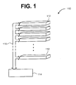
- Figure 1 is an illustration of a multi-level solid state memory device.
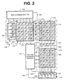
- Figure 2 is an illustration of a level of the solid state memory device, the level including address logic.
- Figures 3a-3c are illustrations of different types of programmable elements in the level.
- Figure 4 is another illustration of a programmable element.
- Figure 4a is an illustration of a method of forming the address logic.
- Figure 5 is an illustration of address patterns for memory lines.
- Figures 5a-5b are illustrations of diode patterns for memory lines.
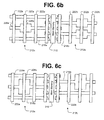
- Figures 6a-6c are illustrations of different layouts for address elements of the address logic.
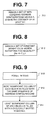
- Figure 7 is an illustration of a first method of generating address configurations for the address logic.
- Figure 8 is an illustration of a second method of generating address configurations for the address logic.
- Figure 9 is an illustration of a method of using a lookup table to extend address configurations for the address logic.
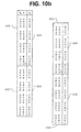
- Figures 10 and 10b illustrate exemplary twin lookup tables.
- the present invention is embodied in a diode-based OTP memory device.
- the structure of the OTP memory device will be described, followed by a description of two address protocols.
- One of the address protocols can provide fault-tolerant address configurations.
- the other address protocol can provide neighborhood-disjoint address configurations, as well as fault-tolerant address configurations.
- Fault-tolerant address logic can improve manufacturing yields, and neighborhood-disjoint address logic allows the memory device to be formed at higher resolution.
- the description of the address protocols will be followed by a description of a method of using a lookup tale to extend the address configurations to large memory arrays.
- FIG. 1 shows a multi-level solid state memory device 110. Multiple levels 112 are stacked on top of one another. Each level 112 includes main memory and address logic. The levels 112 are connected to control/interface circuitry 114 by a memory system interface 116. The control/interface circuitry 114 is formed in a substrate. The control/interface circuitry 114 performs error code correction (ECC) and defect management functions, as well as functions for operating the device 110. These functions include setting write voltages, setting write enable lines and controlling power sense striping, addressing the memory by converting logical addresses to address line patterns required to access physical memory locations, and data read processing of sense line outputs.
- ECC error code correction
- the system interface 116 includes address lines. Address logic on each level 112 shares the same address lines. When data is written to the device 110, the bits are not stored in contiguous memory elements on a level. Instead, the bits of a word are stored on different levels 112.
- address logic is fault tolerant, one address line could be defective in one level, and another address line could be defective at another level, but each level would independently tolerate the defects.
- the level 208 includes main memory 210 and programmable address logic 212, 214.
- the main memory 210 includes a cross point resistive array of OTP memory elements 216, word lines 218 extending along rows of the memory elements 216, and bit lines 220 extending along columns of the memory elements 216. There may be one word line 218 for each row of the memory elements 216 and one bit line 220 for each column of the memory elements 216.
- Each memory element 216 is located at a cross point of a word line 218 and a bit line 220. Only a relatively small number of memory elements 216 is shown to simplify the illustration of the level 208. In practice, arrays of any size may be used.
- a memory line may refer to either a word line 218 or a bit line 220.
- the address logic 212, 214 uses combinatorial diode logic to address the memory elements 216 during read and write operations.
- the address logic 212, 214 includes an OTP row decoder 212 for selecting the word lines 218.
- the row decoder 212 selects the word lines 218 by decoding addresses supplied on row address lines 222 (the addresses may be supplied by external row address drivers 224).
- the row decoder 212 includes a plurality of OTP address elements 226. Each address element 226 of the row decoder 212 is at a cross point of a word line 218 and a row address line 222.
- the address logic 212, 214 also includes an OTP column decoder 214 for selecting the bit lines 220.
- the column decoder 214 selects the bit lines 220 by decoding addresses supplied on column address lines 228 (the addresses may be supplied by external column address drivers 230).
- the column decoder 214 also includes a plurality of OTP address elements 226. Each address element 226 of the column decoder 214 is at the cross point of a bit line 220 and a column address line 228.
- each word line 218 terminates at row sense logic 234.
- the row sense logic 234 includes multiple sense resistors 236, each sense resistor 236 connected between a row power line 238 and an end of a word line 218.
- a row sense line 240 crosses the word lines 218.
- the row sense logic 234 also includes multiple sense elements 242, each sense element 242 connected between the row sense line 240 and a word line 218.
- each bit line 220 terminates at column sense logic 244.
- the column sense logic 244 includes multiple sense resistors 236, each sense resistor 236 connected between a column power line 246 and an end of a bit line 220.
- a column sense line 248 crosses the bit lines 220.
- the column sense logic 244 also includes multiple sense elements 242, each sense element 242 connected between the column sense line 248 and a bit line 220.
- a row programming line 250 between the main memory 210 and the row decoder 212, crosses the word lines 218.
- Programming elements 252 are connected between the row programming line 250 and the word lines 218.
- Programming elements 252 are connected between the column programming line 254 and the bit lines 220.
- the memory elements 216, the address elements 226, the sense elements 242 and the programming elements 252 may all be diode-based. This simplifies the fabrication of the level 208.
- the programmable element of Figure 3a includes a fuse 310 coupled in series with a diode 312. Prior to programming, the resistance state of such an element is low, with the fuse 310 intact. During programming, the resistance state of the element can be changed from low to high by "blowing" the fuse 310.
- the programmable element of Figure 3b includes a resistor 320 coupled in series with a diode 322. Prior to programming, the resistance state of such an element is low, with the resistor 320 intact. During programming, the resistance state of the element can be changed from low to high by "blowing" the resistor 320.
- the programmable element of Figure 3c includes only a diode 332. Prior to programming, the diode 332 is intact, whereby its resistance state is low. During programming, the diode 332 can be opened to change its resistance state from low to high. Such a diode 332 functions as a fuse. In the alternative, the diode 332 can function as an anti-fuse, going from a high resistance state to a low resistance state during programming.
- the programmable elements 216/226/242/252 are not limited to the types shown in Figures 3a-3c.
- the programmable elements 216/226/242/252 could include transistors instead of diodes.
- the level 208 may be fabricated as follows. Column lines 220 are formed on a substrate, a multi-layer film of silicon is formed on the column lines 220, and word lines 218 are formed on the film.
- Each programmable element 216/226/242/252 may be formed as that portion of the film (F) between two crossing traces (T) (see Figure 4). The size of the programmable element 216/226/242/252 is determined by the overlapping area between crossing lines and the thickness of the film.
- a diode in main memory 210 may be formed as that portion of the film between crossing word and bit lines 218 and 220.
- the different layers of the film have appropriate dopings (and/or a combination of crystalline and amorphous silicon) to form the diodes 312, 322, 332. Additional layers with appropriate dopings can be added to form resistors 320, fuses 310, or anti-fuses.
- the sense resistors 236 may be formed by modifying the ends of the word and bit lines 218 and 220.
- the row and column address drivers 224 and 230 may be formed on the substrate, as part of the control/interface circuitry 114.
- Data may be written to the main memory 210 by supplying row and column addresses to the row and column decoders 212 and 214.
- a write current flows through a selected word line 218 and a selected bit line 220 and, therefore, flows through the memory element 216 at the cross point of the selected word and bit lines 218 and 220.
- Magnitude of the write current is sufficient to change the resistance state of the selected element (e.g., by opening the fuse 310 of Figure 3a, opening the resistor 320 of Figure 3b, opening the diode 332 of Figure 3c, shorting the anti-fuse).
- the resistance state of a memory element 216 may be sensed by supplying row and column addresses to the row and column decoders 212 and 214. A voltage is applied to the row sense line 240 and a voltage of opposite polarity is applied to the column sense line 248. A sense current flows through a selected word line 218 and a selected bit line 220 and, therefore, flows through the memory element 216 at the cross point of the selected word and bit lines 218 and 220. Magnitude of the sense current indicates the resistance state of the selected memory element 216.
- the row and column decoders 212 and 214 may be configured (410) prior to device fabrication (412), and programmed (414) after the level 208 has been fabricated.
- the decoders 212 and 214 may be configured by assigning address configurations to memory lines. Each address configuration contains a bit pattern of logic 1's and logic 0's. Each bit in an address configuration corresponds to a programmable address element 226 connected to a memory line.
- the address elements 226 are fabricated according to the address configurations. For example, an address element 226 corresponding to an address configuration bit value of '0' has a different current-carrying capability than an address elements 226 corresponding to an address configuration bit value of '1'. Fabrication and programming of the address elements will now be described in greater detail. Address protocols for generating the address configurations will be discussed later.
- the higher current-carrying capability elements, indicated by filled-in zeros (•), correspond to a first logic value of an address configuration bit.
- the address elements 226 indicated by filied-in zeros will not have their resistance states changed during programming.
- the address elements indicated by crosses will have their resistance states changed during programming.
- the elements indicated by crosses correspond to logic '0' and the elements indicated by filled-in zeros correspond to a logic '1'.
- a logic '1' does not necessarily correspond to a high voltage.
- a voltage (-V) is applied across the row programming line 250, and a voltage of opposite polarity (+V) is applied to the row sense line 240.
- a voltage is applied across the column programming line 254, and a voltage of opposite polarity is applied to the column sense line 248.
- This will effectively apply a voltage across two diodes connected back-to-back. The voltage is applied in such a manner that all address elements are reversed-biased and the sense elements are forward-biased. Consequently, a current flows through the address elements 226.
- the memory lines M1-M9 for the row decoder 212 are connected to different patterns of intact and changed address elements 226, such that a set of address lines that will de-select all but one of the memory lines.
- Figure 5a shows a diode pattern for a memory line (after programming).
- the address elements 226b having the higher current-carrying capability may be made physically larger than the address elements 226a having the lower current-carrying capability. If an address protocol can guarantee that no column has adjacent enlarged address elements 226b, then the address logic may have the configuration shown in Figure 6a.
- Figure 6a shows a row decoder 212 in which columns do not contain any adjacent enlarged address elements 226b. Although not shown as such, the address elements 226a and 226b may be formed at full contact pitch.
- the address protocol cannot provide such a guarantee, whereby the address logic could include adjacent enlarged address elements in a column, the distance between word lines 18 may be increased. However, this would reduce the data storage density of the main memory.
- the row decoder 212 may be divided into two spaced-apart sets 212a and 212b, as shown in Figure 6b. Odd-numbered word lines 218a are interdigitated with even-numbered word lines 218b. A first set of address lines 222a crosses the odd-numbered word lines 218a, and a second set of address lines 222b crosses the even-numbered word lines 218b. The first and second sets of address lines 222a and 222b receive the same address signal.
- Figures 6a-6c were just described in connection with the row decoder 212. However, the same principles may be applied to the column decoder 214.
- the address protocol involves a 1:1 mapping of n-bit address configurations to each one of L memory lines (e.g., L rows or L columns) so that no two rows are assigned the same address configuration and that no two columns are assigned the same address configuration.
- L memory lines e.g., L rows or L columns
- an address line can be rendered unusable by a single defective connection on any of the layers.
- An address line might be rendered unusable by defects occurring over time due to aging or environmental processes. If one of the address lines A0, A1, A2 or A3 becomes unusable, that address line will be unable to de-select certain memory lines. If address line A3 becomes defective, it will not be able to de-select memory lines M2, M4 and M6.
- the fault-tolerance has a built-in redundancy that allows the memory device to function correctly even if defects arise. Thus the fault tolerance can improve manufacturing yields.
- the cost is an increase in address lines.
- Fault-tolerance may be achieved by assigning a set of non-covering address configurations having a symmetric distance of at least t+1, where t is the maximum allowable number of defective address lines (710).
- the unidirectional distance d U (u 1 , u 2 ) is the number of positions where u 1 has 1's and u 2 has 0's.
- the symmetric distance ds(U) is the minimum symmetric between any two distinct words in the set U
- the Hamming distance is d H (U) is the minimum Hamming distance between any two distinct words in the set U.
- Memory lines are assigned address configurations such that no address configuration covers the other. This constraint prevents a single address from selecting more than one memory line.
- the set of words may be assigned as address configurations for n address lines.
- a t-Sperner(n,L) code is a set U that consists of L n-bit words, such that d S (U) ⁇ t+1.
- the address words may be constant weight code (CWC) words, which are a type of t-Sperner words.
- CWC constant weight code
- a set C of n-bit words is a CWC (n,2t+2,w) if each word in the set C has a Hamming weight (w) and d H (C) ⁇ 2t+2.
- address line A1 becomes unusable, the remaining six address lines A0 and A2-A6 will be able to unambiguously select each of the six memory lines M1-M6.
- the memory device may be fabricated at a higher resolution by using an address protocol that generates neighborhood-disjoint address configurations. Such an address protocol guarantees that no column has adjacent enlarged address elements 226b.
- the neighborhood-disjoint address configurations are generated by assigning a set of constant weight code words satisfying the inequality (2w +t+1) ⁇ n, where w is the weight of the code words, n is the number of address lines, and t is the maximum allowable number of defective address lines (810).
- the operator ⁇ represents a bit-wise "AND.”
- the address configuration assigned to the k th memory line (Mk) is selected randomly from the remaining code words that are neighborhood-disjoint with the configuration assigned to the k-1 th memory line. If a neighborhood-disjoint code word cannot be found among the remaining code words, the k-1 th address configuration is deleted, and another selection for the k-1 th address configuration is made. Then the k th address configuration is selected.
- the address configurations may be assigned to the memory lines by using a lookup table.
- the lookup table could provide all of the n-bit address configurations for a memory device having n address lines and L memory lines.
- a lookup table can become prohibitively large as storage capacity of the memory device is increased.
- Figure 9 illustrates a method involving a lookup table that provides a sequence of n-bit address configurations for n address lines and L memory lines.
- the method includes using the lookup table to generate address configurations for 2n address lines and L 2 memory lines.
- a total of L blocks is formed (910).
- a “most significant column” will refer to the left half of each block.
- a “least significant column” will refer to the right half of each block.
- the most significant column of each block is filled with the sequence such that the most significant column of each block contains the same sequence (912).
- the i th entry in the most significant column of each block is equal to the i th entry of the lookup table.
- the least significant column of each block is filled with the sequence such that the sequence in the second block is shifted cyclically with respect to the sequence in the first block, the sequence in the third block is shifted cyclically with respect to the sequence in the second block, and so on (914).
- the sequences are cyclically shifted such that the i th entry in the least significant column of the k th block is equal to the (i+s(k)) th entry of the lookup table, where s(k) is the amount of shift in the k th block relative to the first block. L should be subtracted from i+s(k) when this sum is greater than L.
- the cyclical shift s(k) for each block (k) is distinct.
- the L blocks contain address configurations for L 2 memory lines and 2n address lines.
- the address configurations form the sequence ABC, where A, B and C represent 3-bit configurations 001 b , 010 b , and 100 b , respectively.
- the most significant column (b 0 ) of each block has the same unshifted sequence (ABC), with the entry in the i th most significant column being the same as the i th entry of the lookup table of Table 4.
- the sequence of each block in the least significant column (b 1 ) is shifted.
- the neighborhood-disjoint property is maintained in this larger addressing protocol.
- the most significant column (b 0 ) of each block has the same sequence (ABCD), with the i th entry in each most significant column (b 0 ) being the same as the i th entry of the sequence.
- the sequence in the least significant column (b 1 ) changes its phase at each block.
- the neighborhood-disjoint property is maintained in this larger addressing protocol, except that the last 2n-bit configuration is disjoint from the first one.
- the neighborhood-disjoint property does not hold cyclically, unless the n-bit configuration address A** is replaced by an n-bit configuration address that is neighborhood-disjoint with the configuration addresses D and A.
- twin tables will now have three columns (b 0 , b 1 and b 2 ) and will have the structure shown in Figures 10a and 10b.
- the column on the right is concatenated to the column on the left.
- Numeral 1010_ refers to the block containing the first two columns of Table 6
- numeral 1012_ refers to the block containing the first two columns of Table 7.
- Numeral 1014 refers to the sequence ABCD repeated four times
- numeral 1016 refers to the sequence CDAB repeated four times
- numeral 1018 refers to the sequence DABC repeated four times
- numeral 1020 refers to the sequence BCDA repeated four times
- the method of Figure 9 can be further extended to L 4 memory lines and 4n address lines, and so on.
- the method of Figure 9 is not limited to extending the fault-tolerant and/or neighborhood-disjoint address configurations generated by the methods shown in Figures 7 and 8.
- the address configurations may be generated by other methods as well.
- the address protocols described above are not limited to the memory device described above. They may be applied to any memory device using combinatorial address logic.
Landscapes
- Engineering & Computer Science (AREA)
- Microelectronics & Electronic Packaging (AREA)
- Theoretical Computer Science (AREA)
- Physics & Mathematics (AREA)
- General Engineering & Computer Science (AREA)
- General Physics & Mathematics (AREA)
- For Increasing The Reliability Of Semiconductor Memories (AREA)
- Read Only Memory (AREA)
- Static Random-Access Memory (AREA)
- Techniques For Improving Reliability Of Storages (AREA)
Applications Claiming Priority (2)
| Application Number | Priority Date | Filing Date | Title |
|---|---|---|---|
| US09/990,924 US6466512B1 (en) | 2001-11-13 | 2001-11-13 | Method of generating address configurations for solid state memory |
| US990924 | 2001-11-13 |
Publications (2)
| Publication Number | Publication Date |
|---|---|
| EP1310960A2 true EP1310960A2 (de) | 2003-05-14 |
| EP1310960A3 EP1310960A3 (de) | 2005-01-12 |
Family
ID=25536657
Family Applications (1)
| Application Number | Title | Priority Date | Filing Date |
|---|---|---|---|
| EP02257803A Withdrawn EP1310960A3 (de) | 2001-11-13 | 2002-11-13 | Adressenkonfiguration für Halbleiterspeicher |
Country Status (6)
| Country | Link |
|---|---|
| US (1) | US6466512B1 (de) |
| EP (1) | EP1310960A3 (de) |
| JP (1) | JP4081350B2 (de) |
| KR (1) | KR20030040101A (de) |
| CN (1) | CN100380518C (de) |
| TW (1) | TW580711B (de) |
Families Citing this family (13)
| Publication number | Priority date | Publication date | Assignee | Title |
|---|---|---|---|---|
| US6535455B1 (en) * | 2001-10-13 | 2003-03-18 | Hewlett-Packard Company | Fault-tolerant neighborhood-disjoint address logic for solid state memory |
| US7003713B2 (en) * | 2002-05-16 | 2006-02-21 | Broadcom Corporation | Variable Hamming error correction for a one-time-programmable-ROM |
| US7350132B2 (en) * | 2003-09-10 | 2008-03-25 | Hewlett-Packard Development Company, L.P. | Nanoscale interconnection interface |
| US7191380B2 (en) * | 2003-09-10 | 2007-03-13 | Hewlett-Packard Development Company, L.P. | Defect-tolerant and fault-tolerant circuit interconnections |
| US7307345B2 (en) * | 2005-11-01 | 2007-12-11 | Hewlett-Packard Development Company, L.P. | Crossbar-array designs and wire addressing methods that tolerate misalignment of electrical components at wire overlap points |
| WO2006137833A1 (en) * | 2004-08-13 | 2006-12-28 | University Of Florida Research Foundation, Inc. | Nanoscale content-addressable memory |
| US7489583B2 (en) * | 2005-09-06 | 2009-02-10 | Hewlett-Packard Development Company, L.P. | Constant-weight-code-based addressing of nanoscale and mixed microscale/nanoscale arrays |
| US7319416B2 (en) * | 2006-01-30 | 2008-01-15 | Hewlett-Packard Development Company, L.P. | Tunneling-resistor-junction-based microscale/nanoscale demultiplexer arrays |
| US7763978B2 (en) * | 2007-03-28 | 2010-07-27 | Hewlett-Packard Development Company, L.P. | Three-dimensional crossbar array systems and methods for writing information to and reading information stored in three-dimensional crossbar array junctions |
| US7630246B2 (en) * | 2007-06-18 | 2009-12-08 | Micron Technology, Inc. | Programming rate identification and control in a solid state memory |
| KR100892673B1 (ko) | 2007-09-05 | 2009-04-15 | 주식회사 하이닉스반도체 | 어드레스 치환 회로 및 이를 포함하는 반도체 메모리 장치 |
| KR100956946B1 (ko) * | 2008-04-16 | 2010-05-11 | 매그나칩 반도체 유한회사 | 비휘발성 메모리 장치의 쓰기방법 |
| KR100971654B1 (ko) * | 2008-06-25 | 2010-07-22 | (주)아이엘전자 | 플럭스 유입 방지 택트 스위치 |
Family Cites Families (12)
| Publication number | Priority date | Publication date | Assignee | Title |
|---|---|---|---|---|
| US4064558A (en) * | 1976-10-22 | 1977-12-20 | General Electric Company | Method and apparatus for randomizing memory site usage |
| US4092665A (en) * | 1976-12-29 | 1978-05-30 | Xerox Corporation | Method and means for extracting variable length data from fixed length bytes |
| US4556960A (en) * | 1982-12-13 | 1985-12-03 | Sperry Corporation | Address sequencer for overwrite avoidance |
| US4782340A (en) * | 1986-08-22 | 1988-11-01 | Energy Conversion Devices, Inc. | Electronic arrays having thin film line drivers |
| US5550782A (en) * | 1991-09-03 | 1996-08-27 | Altera Corporation | Programmable logic array integrated circuits |
| JPH0696598A (ja) * | 1992-07-10 | 1994-04-08 | Texas Instr Japan Ltd | 半導体メモリ装置及び欠陥メモリセル救済回路 |
| US5721498A (en) * | 1995-12-11 | 1998-02-24 | Hewlett Packard Company | Block segmentation of configuration lines for fault tolerant programmable logic device |
| US6172933B1 (en) * | 1998-09-04 | 2001-01-09 | Intel Corporation | Redundant form address decoder for memory system |
| KR100326268B1 (ko) * | 1998-10-28 | 2002-05-09 | 박종섭 | 디코딩시의동작마진확보를위한디코딩장치및그방법 |
| JP2000285694A (ja) * | 1999-03-30 | 2000-10-13 | Mitsubishi Electric Corp | 半導体記憶装置および半導体記憶装置を搭載する半導体集積回路装置 |
| US6088287A (en) * | 1999-08-23 | 2000-07-11 | Advanced Micro Devices, Inc. | Flash memory architecture employing three layer metal interconnect for word line decoding |
| US6459648B1 (en) * | 2001-10-13 | 2002-10-01 | Josh N. Hogan | Fault-tolerant address logic for solid state memory |
-
2001
- 2001-11-13 US US09/990,924 patent/US6466512B1/en not_active Expired - Lifetime
-
2002
- 2002-10-29 TW TW091132102A patent/TW580711B/zh not_active IP Right Cessation
- 2002-11-07 JP JP2002323686A patent/JP4081350B2/ja not_active Expired - Fee Related
- 2002-11-12 KR KR1020020069929A patent/KR20030040101A/ko not_active Ceased
- 2002-11-13 CN CNB021495300A patent/CN100380518C/zh not_active Expired - Lifetime
- 2002-11-13 EP EP02257803A patent/EP1310960A3/de not_active Withdrawn
Non-Patent Citations (1)
| Title |
|---|
| None * |
Also Published As
| Publication number | Publication date |
|---|---|
| JP2003187589A (ja) | 2003-07-04 |
| US6466512B1 (en) | 2002-10-15 |
| CN1419240A (zh) | 2003-05-21 |
| TW580711B (en) | 2004-03-21 |
| CN100380518C (zh) | 2008-04-09 |
| JP4081350B2 (ja) | 2008-04-23 |
| EP1310960A3 (de) | 2005-01-12 |
| KR20030040101A (ko) | 2003-05-22 |
| TW200300261A (en) | 2003-05-16 |
Similar Documents
| Publication | Publication Date | Title |
|---|---|---|
| EP1288957B1 (de) | Festzustandspeicher | |
| US6990622B2 (en) | Method for error correction decoding in an MRAM device (historical erasures) | |
| US7545689B2 (en) | Method and apparatus for improving yield in semiconductor devices by guaranteeing health of redundancy information | |
| US7944729B2 (en) | Simultaneously writing multiple addressable blocks of user data to a resistive sense memory cell array | |
| US6466512B1 (en) | Method of generating address configurations for solid state memory | |
| US7107507B2 (en) | Magnetoresistive solid-state storage device and data storage methods for use therewith | |
| US6973604B2 (en) | Allocation of sparing resources in a magnetoresistive solid-state storage device | |
| JP2003123486A (ja) | マルチレベル不揮発性メモリ内にデータを記憶および読み出す方法、並びにそのアーキテクチャ | |
| CN112309473B (zh) | 执行数据的状态整形的存储设备 | |
| JP7017495B2 (ja) | フラッシュメモリの管理方法 | |
| US8635426B2 (en) | Diagonally accessed memory array circuit | |
| US6744681B2 (en) | Fault-tolerant solid state memory | |
| US6459648B1 (en) | Fault-tolerant address logic for solid state memory | |
| US20030172339A1 (en) | Method for error correction decoding in a magnetoresistive solid-state storage device | |
| US6535455B1 (en) | Fault-tolerant neighborhood-disjoint address logic for solid state memory | |
| US6535418B2 (en) | Optically programmable address logic for solid state diode-based memory | |
| US20040141389A1 (en) | Solid state storage device and data storage method |
Legal Events
| Date | Code | Title | Description |
|---|---|---|---|
| PUAI | Public reference made under article 153(3) epc to a published international application that has entered the european phase |
Free format text: ORIGINAL CODE: 0009012 |
|
| AK | Designated contracting states |
Designated state(s): AT BE BG CH CY CZ DE DK EE ES FI FR GB GR IE IT LI LU MC NL PT SE SK TR |
|
| AX | Request for extension of the european patent |
Extension state: AL LT LV MK RO SI |
|
| PUAL | Search report despatched |
Free format text: ORIGINAL CODE: 0009013 |
|
| AK | Designated contracting states |
Kind code of ref document: A3 Designated state(s): AT BE BG CH CY CZ DE DK EE ES FI FR GB GR IE IT LI LU MC NL PT SE SK TR |
|
| AX | Request for extension of the european patent |
Extension state: AL LT LV MK RO SI |
|
| RIC1 | Information provided on ipc code assigned before grant |
Ipc: 7G 11C 8/08 B Ipc: 7G 11C 8/10 B Ipc: 7G 11C 8/06 A |
|
| 17P | Request for examination filed |
Effective date: 20050411 |
|
| AKX | Designation fees paid |
Designated state(s): DE |
|
| 17Q | First examination report despatched |
Effective date: 20061130 |
|
| STAA | Information on the status of an ep patent application or granted ep patent |
Free format text: STATUS: THE APPLICATION IS DEEMED TO BE WITHDRAWN |
|
| 18D | Application deemed to be withdrawn |
Effective date: 20090603 |