EP1312936A2 - Dispositif optoélectronique - Google Patents
Dispositif optoélectronique Download PDFInfo
- Publication number
- EP1312936A2 EP1312936A2 EP02025361A EP02025361A EP1312936A2 EP 1312936 A2 EP1312936 A2 EP 1312936A2 EP 02025361 A EP02025361 A EP 02025361A EP 02025361 A EP02025361 A EP 02025361A EP 1312936 A2 EP1312936 A2 EP 1312936A2
- Authority
- EP
- European Patent Office
- Prior art keywords
- optoelectronic device
- light beams
- protective field
- unit
- transmitted light
- Prior art date
- Legal status (The legal status is an assumption and is not a legal conclusion. Google has not performed a legal analysis and makes no representation as to the accuracy of the status listed.)
- Granted
Links
- 230000005693 optoelectronics Effects 0.000 title claims abstract description 50
- 230000001681 protective effect Effects 0.000 claims abstract description 80
- 238000001514 detection method Methods 0.000 claims abstract description 20
- 238000011156 evaluation Methods 0.000 claims abstract description 9
- 238000005259 measurement Methods 0.000 claims description 11
- 238000012360 testing method Methods 0.000 claims description 5
- 230000001360 synchronised effect Effects 0.000 claims description 4
- 230000007613 environmental effect Effects 0.000 claims description 3
- 238000000034 method Methods 0.000 claims description 2
- 230000003287 optical effect Effects 0.000 description 5
- 230000005540 biological transmission Effects 0.000 description 3
- 238000012544 monitoring process Methods 0.000 description 3
- 230000010363 phase shift Effects 0.000 description 3
- 125000004122 cyclic group Chemical group 0.000 description 1
- 230000006378 damage Effects 0.000 description 1
- 230000003247 decreasing effect Effects 0.000 description 1
- 230000001419 dependent effect Effects 0.000 description 1
- 238000011161 development Methods 0.000 description 1
- 230000018109 developmental process Effects 0.000 description 1
- 238000010586 diagram Methods 0.000 description 1
- 239000003973 paint Substances 0.000 description 1
- 230000000737 periodic effect Effects 0.000 description 1
- 238000005070 sampling Methods 0.000 description 1
- 230000035945 sensitivity Effects 0.000 description 1
- 238000007493 shaping process Methods 0.000 description 1
- 238000010972 statistical evaluation Methods 0.000 description 1
- 238000012549 training Methods 0.000 description 1
Images



Classifications
-
- G—PHYSICS
- G01—MEASURING; TESTING
- G01S—RADIO DIRECTION-FINDING; RADIO NAVIGATION; DETERMINING DISTANCE OR VELOCITY BY USE OF RADIO WAVES; LOCATING OR PRESENCE-DETECTING BY USE OF THE REFLECTION OR RERADIATION OF RADIO WAVES; ANALOGOUS ARRANGEMENTS USING OTHER WAVES
- G01S7/00—Details of systems according to groups G01S13/00, G01S15/00, G01S17/00
- G01S7/48—Details of systems according to groups G01S13/00, G01S15/00, G01S17/00 of systems according to group G01S17/00
- G01S7/483—Details of pulse systems
- G01S7/486—Receivers
- G01S7/487—Extracting wanted echo signals, e.g. pulse detection
-
- G—PHYSICS
- G01—MEASURING; TESTING
- G01S—RADIO DIRECTION-FINDING; RADIO NAVIGATION; DETERMINING DISTANCE OR VELOCITY BY USE OF RADIO WAVES; LOCATING OR PRESENCE-DETECTING BY USE OF THE REFLECTION OR RERADIATION OF RADIO WAVES; ANALOGOUS ARRANGEMENTS USING OTHER WAVES
- G01S17/00—Systems using the reflection or reradiation of electromagnetic waves other than radio waves, e.g. lidar systems
- G01S17/02—Systems using the reflection of electromagnetic waves other than radio waves
- G01S17/04—Systems determining the presence of a target
-
- G—PHYSICS
- G01—MEASURING; TESTING
- G01S—RADIO DIRECTION-FINDING; RADIO NAVIGATION; DETERMINING DISTANCE OR VELOCITY BY USE OF RADIO WAVES; LOCATING OR PRESENCE-DETECTING BY USE OF THE REFLECTION OR RERADIATION OF RADIO WAVES; ANALOGOUS ARRANGEMENTS USING OTHER WAVES
- G01S17/00—Systems using the reflection or reradiation of electromagnetic waves other than radio waves, e.g. lidar systems
- G01S17/02—Systems using the reflection of electromagnetic waves other than radio waves
- G01S17/06—Systems determining position data of a target
- G01S17/42—Simultaneous measurement of distance and other co-ordinates
Definitions
- the invention relates to an optoelectronic device according to the preamble of claim 1.
- Such an optoelectronic device is known from DE 44 05 376 C1.
- the optoelectronic device is designed as an area distance sensor and has a transmitter light emitting transmitter and a receiving light beams receiving recipient.
- To determine the positions objects within a two-dimensional protective field become the transmitted light rays deflected via a deflection unit, so that this periodically the Cover the protective field.
- the received light rays reflected from objects are guided to the receiver via the deflection unit.
- the deflection position of the transmitted light beams detected For determination the positions of objects inside and possibly also outside of the protective field is continuously the deflection position of the transmitted light beams detected. Distance measurements are carried out continuously, this preferably being based on the phase measurement principle. This will an amplitude modulation is impressed on the transmitted light beams.
- the object distance is also modulated reception light beams determined. From the distance values obtained in this way and the current ones Deflection positions of the deflection unit and thus of the transmitted light beams the position of the object can be determined.
- the invention has for its object an optoelectronic device of the type mentioned in such a way that with low circuitry Effortlessly capture objects within a Protective field is made possible.
- the optoelectronic device for detecting objects has a light beam emitting within a protective field Transmitter, a receiver receiving receiving light rays, a deflection unit for periodically deflecting the transmitted light beams within the Protective field and an evaluation unit for generating an object detection signal depending on the output signals of the receiver.
- the Optoelectronic device further comprises a modulation unit Modulation of the transmitted light beams with a modulation frequency and a Demodulation unit generating demodulation signals for determining the Phase differences of the transmitted light beams and the received light beams.
- the Modulation frequency is dependent on the deflection angle of the transmitted light beams adjustable to define protective field limits. For generation. of an object detection signal are when an object enters the protective field Changes in the demodulation signals with regard to the protective field limits corresponding values can be recorded.
- the basic idea of the invention is to detect an object within a protective field in the form of a check of injuries Protective field limits.
- the modulation of the transmitted light rays becomes the specification of the protective field limits depending on the deflection positions of the transmitted light beams. This results in a certain phase difference along the protective field boundary of the transmitted light beams and the received light beams, whereby again a predetermined value of that generated in the demodulation unit Demodulation signal is obtained.
- the optoelectronic device Since there is preferably a clear phase relationship within the protective field between the transmitted light beams and received light beams, can with This evaluation clearly determines whether there is an object in the protective field located or not. Accordingly, the optoelectronic device generates a binary object detection signal, whose switching states are a free protective field or an object intervention in the Signal protective field.
- a major advantage of the optoelectronic device according to the invention consists in checking the violation of protective field boundaries can be carried out in a simple manner and with little circuitry complexity is and nevertheless a reliable object detection within the protective field allows.
- a Threshold unit provided for checking the protective field violations.
- At least one threshold value is generated in the threshold value unit by means of of which the demodulation signals are evaluated.
- the threshold value is selected so that it has a predetermined switching distance to the values of the demodulation signals corresponding to the protective field limits having. In the event of a protective field violation in a certain area of the protective field exceed or fall below the corresponding current values of the demodulation signals the threshold, whereby the object detection signal from the switching state "free protective field” to the switching state "object intervention in the protective field "changes.
- An unnecessary change of the switching states of the object detection signal to avoid slight fluctuations in the demodulation signal are preferably two in the threshold value unit forming a switching hysteresis Threshold values generated.
- a reference measurement is preferably carried out cyclically carried out. With this reference measurement are outside the protective field running transmission light beams are guided to the receiver via a test object. The measured values obtained are used to reference the modulation frequency generating modulation unit used.
- the setting generated in the modulation unit is set particularly advantageously Modulation frequency depending on the deflection position of the transmitted light beams such that the values of the Demodulation signals of a phase shift of the transmitted light beams and Receive light beams of approximately 90 °. This makes one special high detection sensitivity when determining protective field violations receive.
- the optoelectronic Device on a deflection unit which is formed by an oscillating mirror, over which only the transmitted light beams are passed.
- the received light rays on the other hand become a receiver via a stationary optical receiver guided.
- This embodiment has a particularly simple and robust Structure, it being particularly advantageous that the adjustment effort for Beam guidance of the transmitted light beams and received light beams within the optoelectronic device is extremely low.
- FIG. 1 shows schematically the structure of an embodiment of the invention optoelectronic device 1.
- the optoelectronic device 1 has a transmitter 3 emitting light beams 2 and one Receiving light beams 4 receiving receiver 5.
- the transmitter 3 exists preferably from a laser diode.
- the receiver 5 preferably consists of a photodiode.
- the optoelectronic device 1 has a deflection unit 6 by means of which the transmitted light beams 2 are periodically deflected. Thereby paint over the transmitted light beams 2 within a predetermined scanning angle range ⁇ a scanning level, which forms a monitoring area.
- the deflection unit 6 in the present case consists of an oscillating mirror, this advantageously being formed by a micromechanical microscan mirror is.
- the received light rays 4 are guided to the receiver 5 via a stationary receiving optics 8.
- receiving optics 8 can be formed by a lens.
- the optical surface of the receiving optics 8 is designed such that Receiving light beams 4 from any segments of the monitoring area are guided to the receiver 5 via the receiving optics 8.
- the optoelectronic device 1 has a modulation unit 9, by means of which the transmitted light beams 2 are modulated with a predetermined modulation frequency.
- the modulation unit 9 can in principle be formed by a synthesizer.
- the modulation unit 9 consists of a voltage-controlled oscillator.
- the modulation frequency generated there can be changed by varying the input voltage U ME of the modulation unit 9.
- the modulation unit 9 is controlled by a microcontroller 10, which is also a component of the evaluation unit of the optoelectronic device 1 and which is used to evaluate the output signals present at the receiver 5.
- a switching output 11 for outputting an object detection signal is on the microcontroller 10 connected.
- one is connected to the microcontroller 10 Serial interface 12 connected via which the optoelectronic device 1 can be parameterized.
- the optoelectronic device 1 has a synchronous rectifier 14 as a demodulation unit.
- the output signals amplified in a broadband amplifier 13 are fed to the synchronous rectifier 14, which is clocked by the modulation unit 9.
- the signals generated there are fed to a low pass 15.
- the demodulation signals U DME present at the output of the low pass 15 provide a measure of the phase shift of the transmitted light beams 2 and the received light beams 4.
- the demodulation signals U DME are finally fed to a threshold value unit 16, in which a digitized signal U S is generated by a threshold value evaluation and is read into the microcontroller 10.
- the optoelectronic device 1 according to FIG. 1 is used to determine whether an object 7 is located within a predetermined protective field 17. Such a thing Protective field 17 is shown in FIG. 2.
- the protective field 17 is part of the the transmitted light beams 2 and is covered by Protective field limits 18 limited.
- the protective field 17 extends over the entire of the scanning light beam 2 swept scan angle range ⁇ . To great distances the protective field 17 is formed by a predetermined contour Protective field limit 18 limited.
- the protective field limits 18 are preferably specified during a Training procedure.
- the protective field limits 18 of an environmental contour such as walls, machines or other stationary facilities.
- the modulation frequency for modulation the transmitted light beams 2 are set in a suitable manner.
- the protective field limits 18 are predetermined by an environmental contour of a machine or the like.
- the modulation frequency of the transmitted light beams 2 is then set by varying the input voltage U ME of the modulation unit 9 such that the demodulation signals U DME each assume a predetermined value which corresponds at least approximately to a phase shift of the transmitted light beams 2 and the received light beams 4 of 90 ° ,
- the setting is made the modulation frequency uniformly in predetermined angle segments of the scan angle range ⁇ .
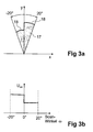
- Figures 3a, b and 4a, b schematically show two different setting options.
- the setting is in these figures the modulation frequencies for the case that the scan angle range is explained ⁇ from -20 ° to + 20 ° in two symmetrical angle segments from -20 ° to 0 ° or is divided from 0 ° to 20 °.
- a constant input voltage U ME is specified for the modulation unit 9 within each angular segment.
- a constant distance value to the optoelectronic device 1 is obtained as the protective field boundary 18 within each angle segment, as can be seen from FIG. 3a.
- the input voltage U ME forms a continuously varying function within the respective angle segment as shown in FIG. 4b as a function of the scan angle ⁇ .
- the demodulation signals U DME generated in the demodulation unit are compared with threshold values S1, S2 generated in the threshold value unit 16.
- threshold values S1, S2 generated in the threshold value unit 16.
- two threshold values S1, S2 forming a switching hysteresis are generated in the threshold value unit 16.
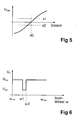
- the threshold values S1 and S2 and the signal curve of the demodulation signal U DME as a function of the distance from the optoelectronic device 1 are shown in FIG. 5.
- the demodulation signal U DME at the protective field boundary 18 assumes the value zero at d 0 .
- the signal values detected with the transmitted light beams 2 are shifted towards smaller distance values, that is to say the demodulation signal U DME takes on negative values as shown in FIG.
- the demodulation signal U DME falls below the value of the threshold value S2
- FIG. 6 The course of the digitized signal U S obtained at the output of the threshold value unit 16 is shown in FIG. 6 for the arrangement according to FIG. 2.
- the arrangement according to FIG 2 is a single object 7 17 within the protection field Consequently, the position of the object 7 in the protective panel 17 as shown in Figure 6 in the angular range between ⁇ 1 and ⁇ 2 according within the angle range between ⁇ min and ⁇ max scan angle range ⁇ registered a protective field violation, that is, the demodulation signal U DME is in this range below the threshold value S2, so that the digitized signal U S assumes the signal value U min . There is no protective field violation in the remaining scan angle range ⁇ .
- the binary object detection signal which can be output via the switching output 11, is generated in the microcontroller 10 on the basis of the digitized signal U S which has been read in.
- the object detection signal has the switching states "free protective field” and "object intervention in the protective field”.
- the object detection signal already takes that Switching state "Object intervention in the protective field” on if within a sampling period, within which the transmitted light beams 2 once the scanning angle range Cover ⁇ , at least one protective field violation is registered.
- the object detection signal only then takes on the switching state "Object intervention in the protective field” if within several successive Scanning periods a protective field violation is registered.
- FIGS. 7a-c show an exemplary embodiment of the optoelectronic device 1 with an advantageous arrangement of optical components, which are integrated in the housing 19 of the optoelectronic device 1.
- the transmitter 3 is a collimation lens for beam shaping of the transmitted light beams 2 20 downstream, which forms a transmission optics.
- the receiving optics 8 have an arrangement from the outside Prism elements 21, an arrangement of internal prism elements 22 and a light guide plate 23.
- the back of the outer prism elements 21 form a flat Light entry surface for the received light beams 4, the light entry surface is flush with the front of the housing 19.
- the inside Prism elements 22 sit on the back of the light guide plate 23.
- the inner and outer prism elements 21, 22 are connected via their tips. In the present case, the prism elements 21, 22 form a reference the receiver 5 concentric arrangement.
- the light guide plate 23 has several layers with different refractive indices. At the back The end of the light guide plate 23 is a deflection element with a deflection mirror 23a provided.
- the transmission light beams 2 pass from the transmitter 3 via the collimation lens 20 to the oscillating mirror forming the deflection unit 6.
- the oscillating mirror is preferably inclined 45 ° to the optical axis of the transmitter 3 and directs the Transmitting light beams 2 from the optoelectronic device 1 through a beam exit window 24 in the housing 19 in the y direction. Due to the periodic deflection of the oscillating mirror, the transmitted light beams 2 in the x direction, for example within a scanning angle range ⁇ deflected by +/- 30 °. Due to the oblique arrangement of the Vibration mirror results in a slightly curved scanning line on the one to be detected Object 7.
- the received light rays 4 reflected by object 7 become via the outer prism elements 21, to the underlying prism elements 22 broken down.
- the prism elements 22 couple the received light beams 4 into the underlying light guide plate 23.
- FIG. 7c shows the beam path of the received light beams 4 in the prism elements 21, 22.
- the light entry surface of the prism element 21 forms a Flat surface in the x-z plane and is parallel to the light exit surface of the prism element 21.
- the refractive angles are at a refractive index of approx. 1.58 for the prism element 21, for example 33 °, and for the prism element 22, for example 45 °, so that all received light beams 4 'to 4 " be broken right away.
- the pointed tips of the prism elements 21 and 22 are not required for beam guidance and are available as mechanical supports available.
- two further deflection mirrors 25 adjoin the light exit window 24, each of which is part of a test object for carrying out cyclic reference measurements.
- the reference measurements serve to reference the input voltages U ME of the modulation unit 9.
- the transmitted light beams 2 guided over the deflection mirrors 25 run outside of the scan angle range ⁇ , so that the object detection by the reference measurements is not affected.
- Each test object does not have 25 more besides the respective deflecting mirror deflection means shown, through which the transmitted light beams 2 completely running within the housing 19 along a defined light path are led to the receiver 5.
- a reference measurement forms a zero distance adjustment, in which the demodulation signal U DME obtained is adjusted to a desired value.
- This can be formed, for example, by one of the threshold values S1 and S2 that are generated in the threshold value unit 16.
- the adjustment to the setpoint is carried out by changing the modulation frequency in the modulation unit 9.
- the adjustment to the setpoint can be based on the principle of interval nesting respectively.
- the current input voltages U ME for generating the modulation frequencies during object detection can be tracked using the reference values determined in the reference measurements.
Landscapes
- Physics & Mathematics (AREA)
- Engineering & Computer Science (AREA)
- Electromagnetism (AREA)
- Computer Networks & Wireless Communication (AREA)
- General Physics & Mathematics (AREA)
- Radar, Positioning & Navigation (AREA)
- Remote Sensing (AREA)
- Optical Radar Systems And Details Thereof (AREA)
- Geophysics And Detection Of Objects (AREA)
Applications Claiming Priority (2)
| Application Number | Priority Date | Filing Date | Title |
|---|---|---|---|
| DE10156660 | 2001-11-17 | ||
| DE10156660 | 2001-11-17 |
Publications (3)
| Publication Number | Publication Date |
|---|---|
| EP1312936A2 true EP1312936A2 (fr) | 2003-05-21 |
| EP1312936A3 EP1312936A3 (fr) | 2005-01-05 |
| EP1312936B1 EP1312936B1 (fr) | 2008-08-20 |
Family
ID=7706186
Family Applications (1)
| Application Number | Title | Priority Date | Filing Date |
|---|---|---|---|
| EP02025361A Expired - Lifetime EP1312936B1 (fr) | 2001-11-17 | 2002-11-14 | Dispositif optoélectronique |
Country Status (2)
| Country | Link |
|---|---|
| EP (1) | EP1312936B1 (fr) |
| DE (1) | DE50212666D1 (fr) |
Cited By (10)
| Publication number | Priority date | Publication date | Assignee | Title |
|---|---|---|---|---|
| WO2006035035A1 (fr) * | 2004-09-28 | 2006-04-06 | Siemens Aktiengesellschaft | Dispositif de surveillance optique de zones tridimensionnelles |
| DE102008020416B3 (de) * | 2008-04-24 | 2009-09-10 | Leuze Electronic Gmbh & Co Kg | Verfahren zur Detektion von Objekten mittels eines Sensors |
| DE102014203379A1 (de) | 2014-02-25 | 2015-08-27 | Ifm Electronic Gmbh | Verfahren zum Betreiben eines optischen Näherungsschalters nach dem Lichtlaufzeitprinzip |
| DE102014203381A1 (de) | 2014-02-25 | 2015-08-27 | Ifm Electronic Gmbh | Verfahren zum Betreiben eines optischen Näherungsschalters nach dem Lichtlaufzeitprinzip |
| EP3078984A1 (fr) * | 2015-04-08 | 2016-10-12 | Sick Ag | Capteur optoelectronique et procede de detection d'objets dans une zone de surveillance |
| DE102018105607A1 (de) * | 2018-03-12 | 2019-09-12 | Sick Ag | Optoelektronischer Sensor und Verfahren zum Erfassen von Objekten in einem Überwachungsbereich |
| CN110988891A (zh) * | 2019-12-26 | 2020-04-10 | 广州市慧建科技有限公司 | 一种激光扫描目标识别系统及方法 |
| DE102019206370A1 (de) * | 2019-05-03 | 2020-11-05 | Audi Ag | Außenleuchteinrichtung für ein Kraftfahrzeug |
| DE102019124266A1 (de) * | 2019-09-10 | 2021-03-11 | Sick Ag | Optoelektronischer Sensor und Verfahren zum Erfassen von Objekten in einem Überwachungsbereich |
| DE102019124265A1 (de) * | 2019-09-10 | 2021-03-11 | Sick Ag | Optoelektronischer Sensor und Verfahren zum Erfassen von Objekten in einem Überwachungsbereich |
Family Cites Families (5)
| Publication number | Priority date | Publication date | Assignee | Title |
|---|---|---|---|---|
| US3649123A (en) * | 1969-04-16 | 1972-03-14 | Holobeam | Variable frequency phase matching distance measuring and positioning device |
| EP0569686B1 (fr) * | 1992-05-09 | 1997-06-04 | Leuze electronic GmbH + Co. | Dispositif de surveillance comportant un émetteur, un récepteur et un circuit d'analyse de signal |
| DE4405376C1 (de) * | 1994-02-19 | 1995-02-16 | Leuze Electronic Gmbh & Co | Verfahren zum Erfassen von Objekten in einem Überwachungsbereich |
| US6052190A (en) * | 1997-09-09 | 2000-04-18 | Utoptics, Inc. | Highly accurate three-dimensional surface digitizing system and methods |
| DE19828000C2 (de) * | 1998-06-24 | 2000-06-21 | Schmersal Eot Gmbh & Co Kg | Verfahren zur optoelektronischen Überwachung eines Schutzbereichs |
-
2002
- 2002-11-14 DE DE50212666T patent/DE50212666D1/de not_active Expired - Fee Related
- 2002-11-14 EP EP02025361A patent/EP1312936B1/fr not_active Expired - Lifetime
Cited By (22)
| Publication number | Priority date | Publication date | Assignee | Title |
|---|---|---|---|---|
| WO2006035035A1 (fr) * | 2004-09-28 | 2006-04-06 | Siemens Aktiengesellschaft | Dispositif de surveillance optique de zones tridimensionnelles |
| US7701557B2 (en) | 2004-09-28 | 2010-04-20 | Siemens Aktiengesellschaft | Device for monitoring spatial areas |
| DE102008020416B3 (de) * | 2008-04-24 | 2009-09-10 | Leuze Electronic Gmbh & Co Kg | Verfahren zur Detektion von Objekten mittels eines Sensors |
| EP2112530A3 (fr) * | 2008-04-24 | 2013-08-28 | Leuze electronic GmbH + Co. KG | Procédé de détection d'objets à l'aide d'un capteur |
| DE102014203379A1 (de) | 2014-02-25 | 2015-08-27 | Ifm Electronic Gmbh | Verfahren zum Betreiben eines optischen Näherungsschalters nach dem Lichtlaufzeitprinzip |
| DE102014203381A1 (de) | 2014-02-25 | 2015-08-27 | Ifm Electronic Gmbh | Verfahren zum Betreiben eines optischen Näherungsschalters nach dem Lichtlaufzeitprinzip |
| DE102014203379B4 (de) | 2014-02-25 | 2018-05-30 | Ifm Electronic Gmbh | Verfahren zum Betreiben eines optischen Näherungsschalters nach dem Lichtlaufzeitprinzip |
| DE102014203381B4 (de) | 2014-02-25 | 2023-11-02 | Ifm Electronic Gmbh | Verfahren zum Betreiben eines optischen Näherungsschalters nach dem Lichtlaufzeitprinzip |
| EP3078984A1 (fr) * | 2015-04-08 | 2016-10-12 | Sick Ag | Capteur optoelectronique et procede de detection d'objets dans une zone de surveillance |
| DE102015105263A1 (de) * | 2015-04-08 | 2016-10-13 | Sick Ag | Optoelektronischer Sensor und Verfahren zur Erfassung von Objekten in einem Überwachungsbereich |
| EP3540459A1 (fr) * | 2018-03-12 | 2019-09-18 | Sick AG | Capteur optoélectronique et procédé de détection d'objets dans une zone de surveillance |
| US10921183B2 (en) | 2018-03-12 | 2021-02-16 | Sick Ag | Optoelectronic sensor and method for detecting objects in a monitored zone |
| DE102018105607B4 (de) | 2018-03-12 | 2022-05-25 | Sick Ag | Optoelektronischer Sensor und Verfahren zum Erfassen von Objekten in einem Überwachungsbereich |
| DE102018105607A1 (de) * | 2018-03-12 | 2019-09-12 | Sick Ag | Optoelektronischer Sensor und Verfahren zum Erfassen von Objekten in einem Überwachungsbereich |
| DE102019206370A1 (de) * | 2019-05-03 | 2020-11-05 | Audi Ag | Außenleuchteinrichtung für ein Kraftfahrzeug |
| US12325349B2 (en) | 2019-05-03 | 2025-06-10 | Audi Ag | External lighting device for a motor vehicle |
| DE102019206370B4 (de) | 2019-05-03 | 2026-03-05 | Audi Ag | Außenleuchteinrichtung für ein Kraftfahrzeug |
| DE102019124266A1 (de) * | 2019-09-10 | 2021-03-11 | Sick Ag | Optoelektronischer Sensor und Verfahren zum Erfassen von Objekten in einem Überwachungsbereich |
| DE102019124265A1 (de) * | 2019-09-10 | 2021-03-11 | Sick Ag | Optoelektronischer Sensor und Verfahren zum Erfassen von Objekten in einem Überwachungsbereich |
| EP3792668A1 (fr) | 2019-09-10 | 2021-03-17 | Sick Ag | Capteur optoélectronique et procédé de détection des objets dans une zone de surveillance |
| DE102019124265B4 (de) | 2019-09-10 | 2023-08-10 | Sick Ag | Optoelektronischer Sensor und Verfahren zum Erfassen von Objekten in einem Überwachungsbereich |
| CN110988891A (zh) * | 2019-12-26 | 2020-04-10 | 广州市慧建科技有限公司 | 一种激光扫描目标识别系统及方法 |
Also Published As
| Publication number | Publication date |
|---|---|
| EP1312936B1 (fr) | 2008-08-20 |
| EP1312936A3 (fr) | 2005-01-05 |
| DE50212666D1 (de) | 2008-10-02 |
Similar Documents
| Publication | Publication Date | Title |
|---|---|---|
| EP1405037B1 (fr) | Dispositif de mesure optique de distance sur une plage de mesure etendue | |
| EP2002281B1 (fr) | Dispositif de mesure optique de distances | |
| DE10124433A1 (de) | Vorrichtung zur optischen Distanzmessung | |
| EP1789754A1 (fr) | Dispositif et procede de mesure de distance optique | |
| DE102006013290A1 (de) | Vorrichtung zur optischen Distanzmessung sowie Verfahren zum Betrieb einer solchen Vorrichtung | |
| DE10336458A1 (de) | System zur Abstandsmessung mittels Lichtquellen | |
| EP1152259B1 (fr) | Télémètre optique | |
| DE4215272C2 (de) | Einen Sender, einen Empfänger und eine Schaltungsanordnung zur Signalauswertung aufweisende lichtelektrische Überwachungseinrichtung | |
| EP1312936B1 (fr) | Dispositif optoélectronique | |
| DE10232878A1 (de) | Vorrichtung und Verfahren zur Distanzmessung | |
| DE202022104647U1 (de) | Optischer Sensor | |
| WO2005064359A1 (fr) | Dispositif pour mesurer la distance a des objets proches et eloignes | |
| DE10041182C2 (de) | Optoelektronische Vorrichtung | |
| EP1624278B1 (fr) | Ressort pneumatique comprenant un dispositif de mesure pour déterminer la distance de pièces d'un véhicule automobile | |
| DE3750292T2 (de) | Optischer Verschiebungsaufnehmer. | |
| EP0610374B1 (fr) | Procede pour la mesure des inclinaisons d'interfaces dans un systeme optique | |
| WO2018086786A1 (fr) | Détecteur de particules doté d'au moins deux capteurs laser à effet doppler | |
| EP2977786A1 (fr) | Capteur telemetrique destine a la detection et la determination de l'eloignement d'objets | |
| DE4200057A1 (de) | Lasermesssystem zur messung physikalischer messgroessen | |
| EP1329691A2 (fr) | Procédé et dispositif pour la localisation automatique de cibles | |
| DE3917388C1 (fr) | ||
| EP3336583B1 (fr) | Télémètre à laser | |
| DE19511990A1 (de) | Verfahren und Vorrichtung zur Erzeugung und Erfassung modulierter Signale | |
| DE202006006482U1 (de) | Optischer Sensor | |
| DE102018104404B4 (de) | Optoelektronischer Sensor und Verfahren zum Erfassen eines Objekts |
Legal Events
| Date | Code | Title | Description |
|---|---|---|---|
| PUAI | Public reference made under article 153(3) epc to a published international application that has entered the european phase |
Free format text: ORIGINAL CODE: 0009012 |
|
| 17P | Request for examination filed |
Effective date: 20021129 |
|
| AK | Designated contracting states |
Designated state(s): AT BE BG CH CY CZ DE DK EE ES FI FR GB GR IE IT LI LU MC NL PT SE SK TR |
|
| AX | Request for extension of the european patent |
Extension state: AL LT LV MK RO SI |
|
| PUAL | Search report despatched |
Free format text: ORIGINAL CODE: 0009013 |
|
| AK | Designated contracting states |
Kind code of ref document: A3 Designated state(s): AT BE BG CH CY CZ DE DK EE ES FI FR GB GR IE IT LI LU MC NL PT SE SK TR |
|
| AX | Request for extension of the european patent |
Extension state: AL LT LV MK RO SI |
|
| AKX | Designation fees paid |
Designated state(s): AT BE BG CH CY CZ DE DK EE ES FI FR GB GR IE IT LI LU MC NL PT SE SK TR |
|
| 17Q | First examination report despatched |
Effective date: 20071213 |
|
| GRAP | Despatch of communication of intention to grant a patent |
Free format text: ORIGINAL CODE: EPIDOSNIGR1 |
|
| RAP1 | Party data changed (applicant data changed or rights of an application transferred) |
Owner name: LEUZE ELECTRONIC GMBH + CO. KG |
|
| GRAS | Grant fee paid |
Free format text: ORIGINAL CODE: EPIDOSNIGR3 |
|
| GRAA | (expected) grant |
Free format text: ORIGINAL CODE: 0009210 |
|
| AK | Designated contracting states |
Kind code of ref document: B1 Designated state(s): BE CH DE FR GB IT LI NL |
|
| REG | Reference to a national code |
Ref country code: GB Ref legal event code: FG4D Free format text: NOT ENGLISH |
|
| REG | Reference to a national code |
Ref country code: CH Ref legal event code: NV Representative=s name: ROTTMANN, ZIMMERMANN + PARTNER AG Ref country code: CH Ref legal event code: EP |
|
| REF | Corresponds to: |
Ref document number: 50212666 Country of ref document: DE Date of ref document: 20081002 Kind code of ref document: P |
|
| PGFP | Annual fee paid to national office [announced via postgrant information from national office to epo] |
Ref country code: NL Payment date: 20081113 Year of fee payment: 7 Ref country code: DE Payment date: 20081203 Year of fee payment: 7 Ref country code: CH Payment date: 20081114 Year of fee payment: 7 |
|
| PGFP | Annual fee paid to national office [announced via postgrant information from national office to epo] |
Ref country code: IT Payment date: 20081120 Year of fee payment: 7 |
|
| PGFP | Annual fee paid to national office [announced via postgrant information from national office to epo] |
Ref country code: FR Payment date: 20081113 Year of fee payment: 7 |
|
| PLBE | No opposition filed within time limit |
Free format text: ORIGINAL CODE: 0009261 |
|
| STAA | Information on the status of an ep patent application or granted ep patent |
Free format text: STATUS: NO OPPOSITION FILED WITHIN TIME LIMIT |
|
| PGFP | Annual fee paid to national office [announced via postgrant information from national office to epo] |
Ref country code: GB Payment date: 20081117 Year of fee payment: 7 |
|
| 26N | No opposition filed |
Effective date: 20090525 |
|
| PGFP | Annual fee paid to national office [announced via postgrant information from national office to epo] |
Ref country code: BE Payment date: 20090126 Year of fee payment: 7 |
|
| BERE | Be: lapsed |
Owner name: LEUZE ELECTRONIC G.M.B.H. + CO. KG Effective date: 20091130 |
|
| REG | Reference to a national code |
Ref country code: NL Ref legal event code: V1 Effective date: 20100601 |
|
| REG | Reference to a national code |
Ref country code: CH Ref legal event code: PL |
|
| GBPC | Gb: european patent ceased through non-payment of renewal fee |
Effective date: 20091114 |
|
| REG | Reference to a national code |
Ref country code: FR Ref legal event code: ST Effective date: 20100730 |
|
| PG25 | Lapsed in a contracting state [announced via postgrant information from national office to epo] |
Ref country code: NL Free format text: LAPSE BECAUSE OF NON-PAYMENT OF DUE FEES Effective date: 20100601 Ref country code: LI Free format text: LAPSE BECAUSE OF NON-PAYMENT OF DUE FEES Effective date: 20091130 Ref country code: FR Free format text: LAPSE BECAUSE OF NON-PAYMENT OF DUE FEES Effective date: 20091130 Ref country code: CH Free format text: LAPSE BECAUSE OF NON-PAYMENT OF DUE FEES Effective date: 20091130 Ref country code: BE Free format text: LAPSE BECAUSE OF NON-PAYMENT OF DUE FEES Effective date: 20091130 |
|
| PG25 | Lapsed in a contracting state [announced via postgrant information from national office to epo] |
Ref country code: DE Free format text: LAPSE BECAUSE OF NON-PAYMENT OF DUE FEES Effective date: 20100601 |
|
| PG25 | Lapsed in a contracting state [announced via postgrant information from national office to epo] |
Ref country code: GB Free format text: LAPSE BECAUSE OF NON-PAYMENT OF DUE FEES Effective date: 20091114 |
|
| PG25 | Lapsed in a contracting state [announced via postgrant information from national office to epo] |
Ref country code: IT Free format text: LAPSE BECAUSE OF NON-PAYMENT OF DUE FEES Effective date: 20091114 |