EP1314099B1 - Vefahren und apparat zur bit-serialer verbindung von hochparallelen prozessormatrizen mit speichermatrizen - Google Patents
Vefahren und apparat zur bit-serialer verbindung von hochparallelen prozessormatrizen mit speichermatrizen Download PDFInfo
- Publication number
- EP1314099B1 EP1314099B1 EP01968297A EP01968297A EP1314099B1 EP 1314099 B1 EP1314099 B1 EP 1314099B1 EP 01968297 A EP01968297 A EP 01968297A EP 01968297 A EP01968297 A EP 01968297A EP 1314099 B1 EP1314099 B1 EP 1314099B1
- Authority
- EP
- European Patent Office
- Prior art keywords
- data
- output
- input
- coupled
- bit
- Prior art date
- Legal status (The legal status is an assumption and is not a legal conclusion. Google has not performed a legal analysis and makes no representation as to the accuracy of the status listed.)
- Expired - Lifetime
Links
Images




Classifications
-
- G—PHYSICS
- G11—INFORMATION STORAGE
- G11C—STATIC STORES
- G11C7/00—Arrangements for writing information into, or reading information out from, a digital store
-
- G—PHYSICS
- G06—COMPUTING OR CALCULATING; COUNTING
- G06F—ELECTRIC DIGITAL DATA PROCESSING
- G06F15/00—Digital computers in general; Data processing equipment in general
- G06F15/76—Architectures of general purpose stored program computers
- G06F15/80—Architectures of general purpose stored program computers comprising an array of processing units with common control, e.g. single instruction multiple data processors
- G06F15/8007—Architectures of general purpose stored program computers comprising an array of processing units with common control, e.g. single instruction multiple data processors single instruction multiple data [SIMD] multiprocessors
-
- G—PHYSICS
- G06—COMPUTING OR CALCULATING; COUNTING
- G06F—ELECTRIC DIGITAL DATA PROCESSING
- G06F15/00—Digital computers in general; Data processing equipment in general
- G06F15/76—Architectures of general purpose stored program computers
- G06F15/78—Architectures of general purpose stored program computers comprising a single central processing unit
- G06F15/7807—System on chip, i.e. computer system on a single chip; System in package, i.e. computer system on one or more chips in a single package
- G06F15/7821—Tightly coupled to memory, e.g. computational memory, smart memory, processor in memory
Definitions
- the present invention relates to the field of computer memory devices and, more particularly to the connection of a massively parallel processor array to a memory array in a bit serial manner to effect a byte wide data reorganization.
- the fundamental architecture used by all personal computers (PCs) and workstations is generally known as the von Neumann architecture, illustrated in block diagram form in Fig. 1 .
- a main central processing unit (CPU) 10 is used to sequence its own operations using a program stored in a memory 12.
- the memory 12, referred to herein as "main memory”, also contains the data on which the CPU 10 operates.
- main memory also contains the data on which the CPU 10 operates.
- a hierarchy of cache memories is usually built into the system to reduce the amount of traffic between the CPU 10 and the main memory 12.
- the von Neumann approach is adequate for low to medium performance applications, particularly when some system functions can be accelerated by special purpose hardware (e.g., 3D graphics accelerator, digital signal processor (DSP), video encoder or decoder, audio or music processor, etc.).
- special purpose hardware e.g., 3D graphics accelerator, digital signal processor (DSP), video encoder or decoder, audio or music processor, etc.
- the approach of adding accelerator hardware is limited by the bandwidth of the link from the CPU/memory part of the system to the accelerator.
- the approach may be further limited if the bandwidth is shared by more than one accelerator.
- the processing demands of large data sets such as those commonly associated with large images, are not served well by the von Neumann architecture.
- the processing demands will not be met even with the conventional accelerator approach.
- the von Neumann architecture has some advantages.
- the architecture contains a homogenous memory structure allowing large memories to be built from many smaller standard units.
- the processing is centralized, it does not matter where the data (or program) resides in the memory.
- the linear execution model is easy to control and exploit.
- Today's operating systems control the allocation of system memory and other resources using these properties.
- the problem is how to improve processing performance in a conventional operating system environment where multiple applications share and partition the system resources, and in particular, the main memory.
- active memory is memory that can do more than store data; it can process it too.
- the active memory looks normal except that it can be told to do something with the data contents and without the data being transferred to the CPU or another part of the system (via the system bus).
- This is achieved by distributing processing elements (PEs) in an array 14 through out the memory structure, which can all operate on their own local pieces of memory in parallel.
- each PE 16 within the PE array 14 typically communicates with each other, as illustrated in Fig. 3 , to exchange data.
- active memory encourages a somewhat different view of the computer architecture, i.e., "memory centered" or viewed from the data rather than the processor.
- a computer system having active memory such as illustrated in Fig. 2
- the work of the CPU 10 is reduced to the operating system tasks, such as scheduling processes and allocating system resources and time.
- Most of the data processing is performed within the memory 12.
- the bandwidth for moving data in and out of memory is greatly increased.
- a large number of parallel processors can be connected to the memory 12 and can operate on their own area of memory independently. Together these two features can provide very high performance.
- SIMD single instruction, multiple data
- MPP massively parallel processor
- SIMD MPP has the advantage that the control overheads of the system are kept to a minimum, while maximizing the processing and memory access bandwidths. SIMD MPPs, therefore, have the potential to provide very high performance very efficiently.
- the hardware consists of many fairly simple repeating elements. Since the PEs are quite small in comparison to a reduced instruction set computer (RISC), they are quick to implement into a system design and their benefit with respect to optimization is multiplied by the number of processing elements. In addition, because the PEs are simple, it is possible to clock them fast and without resorting to deep pipelines.
- RISC reduced instruction set computer
- each PE 16 in the PE array 14 uses only a single pin to connect to the memory 12. Thus, a one bit wide data connection is provided. When this is done, data is stored "bit serially" so that successive bits of a binary value are stored at successive locations in the memory 12. This storage format is referred to as “vertical” storage. Thus data read from and written to each PE will be read and stored, respectively, “vertically” in successive locations in the memory 12 as illustrated in Fig. 4 . Thus, in Fig. 4 , if each PE 16a -16n in a row 22 of PE array 14 is an eight bit PE, i.e., it operates on eight bits of data at a time, the data in the memory will be stored in eight successive vertical locations as illustrated.
- each PE is connected to memory 12 by a one bit wide data connection 24.
- data from PE 16c will be stored in a byte sized area 20 of memory 12 in successive locations in area 20, i.e., it will be stored vertically as illustrated by arrow 30.
- the storage of data bit serially has a number of benefits.
- the number of data wires per PE 16 to the memory 12 is kept to a minimum.
- it allows for variable precision arithmetic to be more easily and efficiently implemented. For example, ten, twelve, or fourteen bit numbers can be stored and processed efficiently.
- Third, in some cases, the difference in speed of the memory access versus the PE cycle time can be matched by serializing the data access.
- Converting between the two formats can be performed within the PE array 14 or within the external device that needs access to the data, but it would be more efficient to store the data in a single format, thus avoiding having to store it in one format and convert it to another.
- the single format would be the normal format used by the external devices.
- US 5473577 discloses a serial memory which internally converts serial input data into to parallel data and writes the data into a memory array two or more bits at a time, and which reads data two or more bits at a time from the memory array and internally converts the read data into serial data for output. Circuits are provided in the memory to allow selective reversing of the order of parallel conversion on the serial input data and of serial conversion on the parallel data read from the memory array. A memory controller is provided to reverse the ascending or descending order of the access address for the memory array in the read and write operations.
- US 5473577 discloses a serial memory which internally converts serial input data into to parallel data and writes the data into a memory array two or more bits at a time, and which reads data two or more bits at a time from the memory array and internally converts the read data into serial data for output. Circuits are provided in the memory to allow selective reversing of the order of parallel conversion on the serial input data and of serial conversion on the parallel data read from the memory array. A memory controller is provided to reverse the ascending or descending order of the access address for the memory array in the read and write operations.
- US 4321694 discloses a circulating shift register memory, particularly adaptable to charge coupled device technology, wherein a plurality of circulating shift registers are arranged to provide a matrix of data bits accessible at a common data front.
- Address counter circuitry cooperating with the register clock circuits selects a particular bit location on the data front for each shift of the shift registers.
- the address counter circuitry provides successive accesses in predetermined patterns, for example along a row, column or diagonal of the bit matrix.
- an active memory device comprising: a main memory; a plurality of processing elements, each of said plurality of processing elements being coupled to a respective portion of said main memory by a single connection; and a circuit, coupled between said main memory and said plurality of elements, for writing data from said plurality of processing elements to said main memory in a horizontal mode and reading data stored in said main memory in a horizontal mode from said main memory to said plurality of processing elements.
- the present invention is an active memory device defined in claims 1 and 3 and in methods defined in claims 10 and 16 and provides methods and apparatus for connecting the processor array of an MPP array to a memory such that data conversion by software is not necessary, and the data can be directly stored in either a normal mode or vertical mode in the memory.
- connection circuit in which multiple PEs share their connections to multiple data bits in the memory array.
- Each PE is associated with a plurality of memory buffer registers, which stores data read from (or to be written to) one or two memory data bits.
- horizontal (normal) mode connection the memory bits are selected so that all the bits of a given byte are stored in the same PE, i.e., each set of buffer registers associated with a respective PE contains one byte as seen by an external device.
- each set of buffer registers contains the successive bits at successive locations in the memory corresponding to that PEs position in the memory word. The selection is achieved utilizing a multiplexer on the input to the register and a pair of tri-state drivers which drive each data line.
- a method and apparatus for connecting the processor array of an MPP to the memory such that data conversion by software is not necessary, and the data can be directly stored in either a normal mode or vertical mode in the memory is provided.
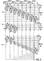
- Fig. 5 illustrates the connection of a processor array of an MPP to a memory in accordance with the present invention.
- eight eight-bit PEs PEO-PE7 share their connections to 64 data bits in the memory array.
- a connection circuit 40a-40h is associated with each PE, i.e., PE0 to PE7, respectively.
- each address Address0 - Address7 from the memory such as for example memory 12 of Fig. 2
- is an eight bit address each having an associated eight bit data line bus 50a-50h. While the description of Fig. 5 is with respect to eight-bit PEs and eight bit data buses, it should be understood that the invention is not so limited and the invention is applicable to any data width, such as for example, ten bit, twelve bits, fourteen bits, etc.
- each data bit line of data bus 50a-50h is connected to a second input of a respective multiplexer 52a-52h in each circuit 40a-40h associated with each PE PE0 - PE7.
- the data bit line for the first bit of data i.e., Bit0
- the data bit line for the second bit of data i.e., Bit1
- the data bit line for the last bit of data i.e., Bit7
- each multiplexer 52a-52h is connected to a respective buffer register 54a-54h.
- the output from each buffer register 54a-54h is connected to a respective input ⁇ 0> - ⁇ 7> of an eight-input multiplexer 60a.
- the output from each buffer register 54a-54h is also connected to the input of a respective pair of tri-state drivers 56a-56h.
- the output PE0 Din 62a from multiplexer 60 is connected to the first PE in the group of eight, i.e., PE0, by a single bit __ connection for passing data from the memory, i.e., Address0-Address7, to PE0
- a second data line, PE Dout 64a is also connected to the single bit connection to receive data from PE0 for writing to the memory into addresses Address0-Address7.
- the data line PE Dout 64a is connected to a first input of each multiplexer 52a-52h.
- the output from the first and second tri-state drivers in pair 56a is connected to a respective bit data line of data bus 50a, i.e., the data bit line associated with the first bit of data Bit0 in Address0.
- the output from the second tri-state driver in pair 56a is connected to a third input of multiplexer 52a.
- the output from the first tri-state driver in pair 56b is connected to a respective data bit line of data bus 50b, i.e., the data bit line associated with the first bit of data Bit0 in Address1, while the output from the second tri-state driver of pair 56b is connected to the second data bit line of data bus 50a and a third input of multiplexer 52b.
- the outputs from the remaining pairs of tri-state drivers 56c-56h are similarly connected, i.e., the output from the first tri-state driver of each pair 56c-56h is connected to its associated bit data line for the first bit of data Bit0 of data bus 50c-50h, while the output from the second tri-state driver of each pair 56c-56h is connected to a third input of its respective multiplexer 52c-52h and also connected to respective bit data lines of data bus 50a.
- the above circuit 40a is substantially duplicated for each of the remaining circuits 40b-40h for each of the PEs in the group, i.e., PE1 - PE7, with the following exception.
- the output from the first and second tri-state drivers in pair 56b is connected to a respective bit data line of data bus 50b, i.e., the bit data line associated with the second bit of data Bit1 from Address1, while the remaining pairs of tri-state drivers 56a and 56c-56h each have the output from the first tri-state driver connected to the bit data line associated with the second bit of data Bit1 of its associated data bus 50a and 50c-50h, respectively, and the output from the second tri-state driver is connected to respective bit data lines of data bus 50b and the third input of its respective multiplexer 52a and 52c-52h.
- the output from the first and second tri-state drivers in pair 56c is connected to the bit data line associated with the third bit of data Bit2 of data bus 50c, while the remaining pairs of tri-state drivers 56a, 56b and 56d-56h each have the output from the first tri-state driver connected to the data bit line associated with the third bit of data Bit2 of its associated data bus 50a, 50b and 50d-50h, respectively, and the output from the second tri-state driver is connected to a respective bit data line of data bus 50c and the third input to its respective multiplexer 52a, 52b and 52d-52h.
- Fig. 5 The operation of the circuitry as illustrated in Fig. 5 is as follows. Suppose for example a read of data is desired, and the data is stored in the memory in a vertical mode, i.e., data will be read from the memory 12 in a vertical fashion, as illustrated in Fig. 4 , to each PE. Thus, it is desired to input each bit from a respective bit in Address0 to Address7 into a respective PE.
- each multiplexer 52a-52h will pass the data on its second input, i.e., data from the respective data buses 50a-50h, to its respective register 54a-54h.
- the first bit of data i.e., Bit0 will be passed through multiplexers 52a-52h to registers 54a-54h, and then to multiplexer 60a.
- Multiplexer 60a will in turn send each bit of data Bit0 serially, i.e., from input ⁇ 0> to input ⁇ 7>, to PE0 via output 62a.
- the output from multiplexer 60a to PE0 will be Bit0 from each of addresses Address0-Address7 i a serial manner.
- the second bit of data i.e., Bit1
- the second bit of data will be passed through multiplexers 52a-52h to registers 54a-54h, and then to multiplexer 60b.
- Multiplexer 60ba will in turn send each bit of data serially, i.e., from input ⁇ 0> to input ⁇ 7>, to PE1 via output 62b.
- the circuits associated with each remaining PE will operate similarly, up to circuit 40h, where the last bit of data, i.e., Bit7, will be passed through multiplexers 52a-52h to registers 54a-54h, and then to multiplexer 60h.
- Multiplexer 60h will in turn send each bit of data serially, i.e., from input ⁇ 0> to input ⁇ 7>, to PE7 via output 62h. Accordingly, the data is provided to each PE from the memory addresses Address0-Address7 in a vertical fashion.
- each data bit from Address0 must be input to PE0 in a serial fashion from Bit0 to Bit7
- each data bit from Address1 must be input to PE1 in a serial fashion from Bit0 to Bit7, and so forth.
- Bit0 on data bit line 0 of bus 50a will be input to the third input of multiplexer 52a
- Bit1 on data bit line 1 of bus 50a will be input to the third input of multiplexer 52b
- Bit2 on data bit line 2 of bus 50a will be input to the third input of multiplexer 52c
- so forth up to Bit7 on data bit line 7 of bus 50a which will be input to the third input of multiplexer 52h.
- Multiplexers 52a-52h will pass the input on its third input to the respective registers 54a-54h.
- the data in registers 54a-54h will be sent to multiplexer 60a.
- Multiplexer 60a will in turn send each bit of data serially, i.e., from input ⁇ 0> to input ⁇ 7>, to PE0 via output 62a.
- PE0 will receive Bit0 to Bit7 from Address0 a single bit at a time.
- Bit0 on data bit line 0 of bus 50b will be input to the third input of multiplexer 52a
- Bit1 on data bit line 1 of bus 50b will be input to the third input of multiplexer 52b
- Bit2 on data bit line 2 of bus 50b will be input to the third input of multiplexer 52c
- so forth up to Bit7 on data bit line 7 of bus 50b which will be input to the third input of multiplexer 52h.
- Multiplexers 52a-52h will pass the input on its third input to the respective registers 54a-54h.
- the data in registers 54a-54h will be sent to multiplexer 60b.
- Multiplexer 60b will in turn send each bit of data serially, i.e., from input ⁇ 0> to input ⁇ 7>, to PE1 via output 62b.
- PE1 will receive Bit0 to Bit7 from Address1 a single bit at a time.
- circuits associated with each remaining PE will operate similarly, up to circuit 40h, where as the data Bit0 to Bit7 from Address7 is provided on bus 50h, Bit0 on data bit line 0 of bus 50h will be input to the third input of multiplexer 52a, Bit1 on data bit line 1 of bus 50h will be input to the third input of multiplexer 52b, Bit2 on data bit line 2 of bus 50h will be input to the third input of multiplexer 52c, and so forth up to Bit7 on data bit line 7 of bus 50h which will be input to the third input of multiplexer 52h.
- Multiplexers 52a-52h will pass the input on its third input to the respective registers 54a-54h. The data in registers 54a-54h will be sent to multiplexer 60h.
- Multiplexer 60h will in turn send each bit of data serially, i.e., from input ⁇ 0> to input ⁇ 7>, to PE7 via output 62h.
- PE7 will receive Bit0 to Bit7 from Address7 a single bit at a time. Accordingly, the data can be read from the memory in a horizontal mode.
- a write is desired in which the data from each PE will be stored in the memory in a vertical mode as illustrated in Fig. 4 .
- the data will be serially output from PE0 on line PE Dout 64, which is connected to the first input of each multiplexer 52a-52h.
- the first bit of data output from PE0 will be passed by multiplexer 52a to register 54a, and then to the pair of tri-state drivers 56a.
- the first tri-state driver of pair 56a will pass the data to data bit line 0 of data bus 50a, which will write the data into the first bit Bit0 of Address 0.
- the second bit of data output from PE0 will be passed by multiplexer 52b to register 54b, and then to the input of the pair of tri-state drivers 56b.
- the first tri-state driver of pair 56b will pass the data to data bit line 0 of data bus 50b, which will write the data into the first bit Bit0 of Address1. This continues for each bit of data from PE0, up to the last bit which is passed by multiplexer 52h to register 54h , and then to the input the pair of tri-state drivers 56h.
- the first tri-state driver of pair 56h will pass the data to data bit line 0 of data bus 50h, which will write the data into the first bit Bit0 of Address7.
- the remaining circuits 40b-40h operate similarly to store the data into the respective location of each address Address0-Address7.
- the first bit of data output from PE1 will be passed by multiplexer 52a to register 54a, and then to the input of the pair or tri-state drivers 56a.
- the first tri-state driver of pair 56a will pass the data to data bit line 1 of data bus 50a, which will write the data into the second bit Bit1 of Address 0.
- the second bit of data output from PE1 will be passed by multiplexer 52b to register 54b, and then to the input of the pair of tri-state drivers 56b.
- the first tri-state driver of pair 56b will pass the data to data bit line 1 of data bus 50b, which will write the data into the second bit Bit1 of Address1. This process continues for each bit of data from PE1 until the second data bit Bit1 of each address Address0-Address7 is filled.
- the first bit of data output from PE7 will be passed by multiplexer 52a to register 54a, and then to the input of the pair of tri-state drivers 56a.
- the first tri-state driver of pair 56a will pass the data to data bit line 7 of data bus 50a, which will write the data into the last bit Bit7 of Address 0.
- the second bit of data output from PE7 will be passed by multiplexer 52b to register 54b, and then to the input of the pair of tri-state drivers 56b.
- the first tri-state driver of pair 56b will pass the data to data bit line 7 of data bus 50b, which will write the data into the last bit Bit7 of Address1. This process continues for each bit of data from PE7 until the last data bit Bit7 of each address Address0-Address7 is filled.
- data can be _ written from each PE to the memory in a vertical mode.
- a write is desired in which the data from each PE will be stored in the memory in a normal mode (horizontal mode) as illustrated in Fig. 4 .
- the data will be serially output from PE0 on line PE Dout 64, which is connected to the first input of each multiplexer 52a-52h.
- the first bit of data output from PE0 will be passed by multiplexer 52a to register 54a, and then to the input of the pair of tri-state drivers 56a.
- the second tri-state driver of pair 56a will pass the data to data bit line 0 of data bus 50a, which will write the data into the first bit Bit0 of Address 0.
- the second bit of data output from PE0 will be passed by multiplexer 52b to register 54b, and then to the input of the pair of tri-state drivers 56b.
- the second tri-state driver of pair 56b will pass the data to data bit line 1 of data bus 50a, which will write the data into the second bit Bit1 of Address0.
- the second tri-state driver of pair 56h will pass the data to data bit line 7 of data bus 50a, which will write the data into the last bit Bit7 of Address0.
- the eight bits of data from PE0 will be written into Bit0 to Bit7 of Address0.
- the remaining circuits 40b-40h operate similarly to store the data into the successive locations of each address Address1-Address7.
- the first bit of data output from PE1 will be passed by multiplexer 52a to register 54a, and then to the input of the pair of tri-state drivers 56a.
- the second tri-state driver of pair 56a will pass the data to data bit line 0 of data bus 50b, which will write the data into the first bit Bit0 of Address1.
- the second bit of data output from PE1 will be passed by multiplexer 52b to register 54b, and then to the input of the pair of tri-state drivers 56b.
- the second tri-state driver of pair 56b will pass the data to data bit line 1 of data bus 50b, which will write the data into the second bit Bit1 of Address1. This process continues for each bit of data from PE1 until the last bit of data from PE1 is written to Bit7 of Address1.
- the first bit of data output from PE7 will be passed by multiplexer 52a to register 54a, and then to the input of the pair of tri-state drivers 56a.
- the second tri-state driver of pair 56a will pass the data to data bit line 0 of data bus 50h, which will write the data into the first bit Bit0 of Address7.
- the second bit of data output from PE7 will be passed by multiplexer 52b to register 54b, and then to the input of the pair of tri-state drivers 56b.
- the second tri-state driver of pair 56b will pass the data to data bit line 1 of data bus 50h, which will write the data into the second bit Bit1 of Address7. This process continues for each bit of data from PE7 until the last data bit Bit7 is written to the last bit Bit7 of Address7. Thus, data can be written to the memory in a horizontal mode.
- data can be read from a memory to a PE and written to the memory from the PE via a single bit connection in either a vertical or horizontal mode.
- a single register 52 such as for example 52a-52h, for each circuit 40a-40h allows only one byte to be held per PE in the memory buffer for either a read or a write operation.
- the use of a second register would allow write data to be held in one while the other is used for a read, or for data pipelining to be done for either.
- Fig. 6 illustrates in schematic diagram form an alternative embodiment of Fig. 5 , in which each register 54a-54h of Fig. 5 is replaced by a pair of registers 80a and 80b. Accordingly, the output from a respective multiplexer 52, i.e., multiplexers 52a-52h of circuits 40a-40h of Fig. 5 , is input to register 80a and register 80b.
- each register 80a and 80b is input to a multiplexer 82.
- the output of multiplexer 82 is sent to a respective multiplexer 60, i.e., multiplexer 60a-60h of Fig. 5 .
- the output from registers 80a and 80b is input to a second muliplexer 84, whose output is connected to a respective pair of tri-state drivers 56, i.e., tri-state drivers 56a-56h of Fig. 5 .
- the operation of the circuit as illustrated in Fig. 6 is similar to that as described with respect to Fig.
- multiplexers 82 and 84 are used to determine from which register 80a or 80b data will be passed to either the input of tri-state driver pair 56 or multiplexer 60. Accordingly, the use of two registers 80a, 80b allows write data to be held in one while the other is used for a read, or for data pipelining to be done for either register.
- An active memory device having the connection circuits 40a-40h of the present invention may be used in a processor-based system 300 of the type shown in Fig. 7 .
- the processor-based system 300 comprises a processor 302 that communicates with the memory device 312 and an I/O device 308 over a bus 320.
- the bus 320 may be a series of buses and bridges commonly used in a processor-based system, but for convenience purposes only, the bus 320 has been illustrated as a single bus.
- the memory device 312 includes connection circuits 40a-40h as previously described with respect to Figs. 5 and 6 .
- the memory device 312 may be a SIMD MPP or any other type of DRAM or SRAM utilizing multiple PEs.
- the processor 302 may itself be an integrated processor which utilizes on-chip memory devices containing the circuitry of the present invention.
- the processor-based system 300 may be a computer system, a process control system or any other system employing a processor and associated memory.
- the processor-based system 300 may also include read-only memory (ROM) 310 and may include peripheral devices such as a floppy disk drive 304 and a compact disk (CD) ROM drive 306 that also communicate with the processor 302 over the bus 320 as is well known in the art.
- ROM read-only memory
- CD compact disk
Landscapes
- Engineering & Computer Science (AREA)
- Computer Hardware Design (AREA)
- Theoretical Computer Science (AREA)
- Computing Systems (AREA)
- General Engineering & Computer Science (AREA)
- Physics & Mathematics (AREA)
- General Physics & Mathematics (AREA)
- Microelectronics & Electronic Packaging (AREA)
- Dram (AREA)
- Multi Processors (AREA)
- Image Processing (AREA)
Claims (19)
- Aktive Speichervorrichtung, umfassend:einen Hauptspeicher,eine Vielzahl von Verarbeitungselementen (PE0 - PE7), wobei jedes der Vielzahl von Verarbeitungselementen durch eine einzelne Bitverbindung an einen jeweiligen Abschnitt des Hauptspeichers gekoppelt ist; undeine Schaltung, die zwischen dem Hauptspeicher und der Vielzahl von Verarbeitungselementen gekoppelt ist, zum Schreiben von Daten von der Vielzahl von Verarbeitungselementen zu dem Hauptspeicher in einem horizontalen Modus, dadurch gekennzeichnet, dass die Schaltung umfasst:wobei die Datenschaltung jedes Bit der Vielzahl von Bits in einem verschiedenen Datenbus, der mit dem Hauptspeicher assoziiert ist, ausgibt und jedes Bit der Vielzahl von Bits in eine Position in dem Hauptspeicher, die mit einer verschiedenen Adresse assoziiert ist, geschrieben wird.eine Vielzahl von Datenschaltungen (40a - 40h), wobei jede der Vielzahl von Datenschaltungen mit einem jeweiligen einen der Vielzahl von Verarbeitungselementen assoziiert ist, jede der Vielzahl von Datenschaltungen konfiguriert ist, um Daten von ihrem jeweiligen Verarbeitungselement zu dem Hauptspeicher hindurchzuleiten, jede der Vielzahl von Datenschaltungen für jede einzelne Bitverbindung umfassend:einen ersten Multiplexer (52a) mit einem ersten Eingang, der an das Verarbeitungselement gekoppelt ist, um eine Vielzahl von Datenbits in einer seriellen Weise (64a) von dem Verarbeitungselement zu empfangen, und einem zweiten Eingang, der an einen Datenbus (50a) der Speichervorrichtung gekoppelt ist;ein erstes Register (54a) mit einem Eingang und einem Ausgang, wobei der Eingang an einen Ausgang des ersten Multiplexers gekoppelt ist;einen zweiten Multiplexer (60a) mit einem Eingang, der an den Ausgang des ersten Registers gekoppelt ist, und einem Ausgang, der an das Verarbeitungselement gekoppelt ist;eine erste Drei-Zustands-Vorrichtung (56a) mit einem Eingang, der an den Ausgang des ersten Registers gekoppelt ist, und einem Ausgang, der an den Datenbus (50a) gekoppelt ist; undeine zweite Drei-Zustands-Vorrichtung (56a) mit einem Eingang, der an den Ausgang des ersten Registers gekoppelt ist, und einem Ausgang, der an den Datenbus und einen dritten Eingang des ersten Multiplexers gekoppelt ist;
- Aktive Speichervorrichtung nach Anspruch 1, wobei die Schaltung weiterhin angepasst ist, um Daten von der Vielzahl von Verarbeitungselementen zu dem Hauptspeicher in einem vertikalen Modus zu schreiben.
- Aktive Speichervorrichtung, umfassend:einen Hauptspeicher,eine Vielzahl von Verarbeitungselementen (PE0 - PE7), wobei jedes der Vielzahl von Verarbeitungselementen durch eine einzelne Bitverbindung an einen jeweiligen Abschnitt des Hauptspeichers gekoppelt ist; undeine Schaltung, die zwischen dem Hauptspeicher und der Vielzahl von Verarbeitungselementen gekoppelt ist, zum Lesen von Daten, die in dem Hauptspeicher, gespeichert sind, in einem horizontalen Modus von dem Hauptspeicher zu der Vielzahl von Verarbeitungselementen, dadurch gekennzeichnet, dass die Schaltung umfasst:wobei jedes Datenbit, das mit einer einzelnen Adresse des Hauptspeichers assoziiert ist, durch ein jeweiliges Register hindurchgeleitet wird und in einen Multiplexer eingegeben wird, der jedes Datenbit in einer seriellen Weise zu dem Verarbeitungselement ausgibt.eine Vielzahl von Datenschaltungen (40a - 40h), wobei jede der Vielzahl von Datenschaltungen mit einer jeweiligen einen der Vielzahl von Verarbeitungselementen assoziiert ist, jede der Vielzahl von Datenschaltungen konfiguriert ist, um Daten von ihrem jeweiligen Verarbeitungselement von dem Hauptspeicher hindurchzuleiten, jede der Vielzahl von Datenschaltungen für jede einzelne Bitverbindung umfassend:einen ersten Multiplexer (52a) mit einem ersten Eingang, der an das Verarbeitungselement gekoppelt ist, um eine Vielzahl von Datenbits in einer seriellen Weise (64a) von dem Verarbeitungselement zu empfangen, und einem zweiten Eingang, der an einen jeweiligen Datenbus (50a) der Speichervorrichtung gekoppelt ist, um ein jeweiliges Datenbit zu empfangen, das mit einer einzelnen Adresse des Hauptspeichers assoziiert ist;ein erstes Register (54a) mit einem Eingang und einem Ausgang, wobei der Eingang an einen Ausgang des ersten Multiplexers gekoppelt ist;einen zweiten Multiplexer (60a) mit einem Eingang, der an den Ausgang des ersten Registers gekoppelt ist, und einem Ausgang, der an das Verarbeitungselement gekoppelt ist;eine erste Drei-Zustands-Vorrichtung (56a) mit einem Eingang, der an den Ausgang des ersten Registers gekoppelt ist, und einem Ausgang, der an den Datenbus (50a) gekoppelt ist; undeine zweite Drei-Zustands-Vorrichtung (56a) mit einem Eingang, der an den Ausgang des ersten Registers gekoppelt ist, und einem Ausgang, der an den Datenbus und einen dritten Eingang des ersten Multiplexers gekoppelt ist;
- Aktive Speichervorrichtung nach Anspruch 3, wobei die Schaltung weiterhin angepasst ist, um Daten, die in dem Hauptspeicher gespeichert sind, in einem vertikalen Modus von dem Hauptspeicher zu der Vielzahl von Verarbeitungselementen zu schreiben.
- Aktive Speichervorrichtung nach einem der vorstehenden Ansprüche, umfassend acht der Verarbeitungselemente.
- Aktive Speichervorrichtung nach einem der vorstehenden Ansprüche, wobei der Ausgang der zweiten Drei-Zustands-Vorrichtung (56a) an einen verschiedenen Datenbus von dem Ausgang der ersten Drei-Zustands-Vorrichtung (56a) gekoppelt ist.
- Aktive Speichervorrichtung nach einem der vorstehenden Ansprüche, die Schaltung weiter umfassend:ein zweites Register mit einem Eingang, der an den Ausgang des ersten Multiplexers (54a) gekoppelt ist;einen dritten Multiplexer mit einem ersten Eingang, einem zweiten Eingang und einem Ausgang, wobei der erste Eingang mit einem Ausgang des zweiten Registers verbunden ist, der Ausgang von dem ersten Register an den zweiten Eingang gekoppelt ist, der Ausgang an den Eingang des zweiten Multiplexers gekoppelt ist; undeinen vierten Multiplexer mit einem ersten Eingang, einem zweiten Eingang und einem Ausgang, wobei der erste Eingang an den Ausgang des ersten Registers gekoppelt ist, der zweite Eingang an den Ausgang des zweiten Registers gekoppelt ist, der Ausgang an den Eingang der ersten und zweiten Drei-Zustands-Vorrichtung gekoppelt ist.
- Aktive Speichervorrichtung nach Anspruch 7, wobei der Ausgang der zweiten Drei-Zustands-Vorrichtung an einen verschiedenen Datenbus von dem Ausgang der ersten Drei-Status-Vorrichtung gekoppelt ist.
- Vezarbeitungssystem, umfassend:eine Verarbeitungseinheit; unddie aktive Speichervorrichtung nach einem der Ansprüche 1 bis 8, die an die Verarbeitungseinheit gekoppelt ist.
- Verarbeitungssystem nach Anspruch 9, wobei die Verarbeitungseinheit und die aktive Speichervorrichtung sich auf demselben Chip befinden.
- Verfahren zum Schreiben von Daten von einem Verarbeitungselement zu einer Speichervorrichtung, die folgenden Schritte umfassend:Bereitstellen einer Vielzahl von Datenbits in einer seriellen Weise von dem Verarbeitungselement zu einer Datenschaltung, umfassend:wobei die Datenschaltung die Daten direkt zu der Speichervorrichtung in einem horizontalen Modus hindurchleitet und wobei der Schritt zum Hindurchleiten der Daten weiter umfasst:einen ersten Multiplexer (52a) mit einem ersten Eingang, der an das Verarbeitungselement gekoppelt ist, und einem zweiten Eingang, der an einen Datenbus der Speichervorrichtung gekoppelt ist;ein erstes Register (54a) mit einem Eingang und einem Ausgang, wobei der Eingang an einen Ausgang des ersten Multiplexers gekoppelt ist;einen zweiten Multiplexer (60a) mit einem Eingang, der an den Ausgang des ersten Registers gekoppelt ist, und einem Ausgang, der an das Verarbeitungselement gekoppelt ist;eine erste Drei-Zustands-Vorrichtung (56a) mit einem Eingang, der an den Ausgang des ersten Registers gekoppelt ist, und einem Ausgang, der an den Datenbus gekoppelt ist; undeine zweite Drei-Zustands-Vorrichtung (56a) mit einem Eingang, der an den Ausgang des ersten Registers gekoppelt ist, und einem Ausgang, der an den Datenbus und einen dritten Eingang des ersten Multiplexers gekoppelt ist;Hindurchleiten der Daten durch die Datenschaltung; undSchreiben der Daten zu der Speichervorrichtung,Ausgeben jedes Bits der Vielzahl von Datenbits von der Datenschaltung in einem verschiedenen Datenbus, der mit der Speichervorrichtung assoziiert ist; undwobei der Schritt zum Schreiben der Daten weiter umfasst, jedes Bit der Vielzahl von Datenbits zu einer Position in der Speichervorrichtung zu schreiben, die mit einer verschiedenen Adresse assoziiert ist.
- Verfahren nach Anspruch 11, wobei der Schritt zum Ausgeben weiter umfasst:Hindurchleiten jedes Bits der Vielzahl von Datenbits durch ein jeweiliges Register.
- Verfahren nach Anspruch 12, wobei jede verschiedene Speicheradresse eine assoziierte Vielzahl von Bits aufweist und wobei der Schritt zum Schreiben jedes Datenbits weiterhin umfasst:Schreiben jedes Datenbits in ein gleiches Bit der assoziierten Vielzahl von Bits in jeder verschiedenen Speicheradresse.
- Verfahren nach Anspruch 11, wobei die Schaltung weiterhin angepasst ist, um mindestens einen Abschnitt der Daten zu der Speichervorrichtung in einem vertikalen Modus hindurchzuleiten.
- Verfahren nach Anspruch 14,
wobei der Schritt zum Schreiben der Daten weiterhin umfasst, jedes Bit der Vielzahl von Datenbits in aufeinanderfolgende Bitpositionen zu schreiben, die mit einer einzelnen Adresse assoziiert sind. - Verfahren nach Anspruch 15, wobei der Schritt zum Ausgeben weiterhin umfasst:Hindurchleiten jedes Bits der Vielzahl von Datenbits durch ein jeweiliges Register.
- Verfahren zum Lesen von Daten, die in einer Speichervorrichtung gespeichert sind, und Bereitstellen der Daten zu einem Verarbeitungselement, das Verfahren die folgenden Schritte umfassend:Bereitstellen einer Vielzahl von Datenbits von der Speichervorrichtung zu einer Datenschaltung, umfassend:einen ersten Multiplexer (52a) mit einem ersten Eingang, der an das Verarbeitungselement gekoppelt ist, und einem zweiten Eingang, der an einen Datenbus der Speichervorrichtung gekoppelt ist;ein erstes Register (54a) mit einem Eingang und einem Ausgang, wobei der Eingang an einen Ausgang des ersten Multiplexers gekoppelt ist;einen zweiten Multiplexer (60a) mit einem Eingang, der an den Ausgang des ersten Registers gekoppelt ist, und einem Ausgang, der an das Verarbeitungselement gekoppelt ist;eine erste Drei-Zustands-Vorrichtung (56a) mit einem Eingang, der an den Ausgang des ersten Registers gekoppelt ist, und einem Ausgang, der an den Datenbus gekoppelt ist; undeine zweite Drei-Zustands-Vorrichtung (56a) mit einem Eingang, der an den Ausgang des ersten Registers gekoppelt ist, und einem Ausgang, der an den Datenbus und einen dritten Eingang des ersten Multiplexers gekoppelt ist;und Hindurchleiten der Daten durch die Datenschaltung;wobei die Daten in der Speichervorrichtung in einem horizontalen Modus gespeichert werden und wobei der Schritt zum Hindurchleiten der Daten weiterhin umfasst:Hindurchleiten jedes Datenbits, das mit einer einzelnen Adresse assoziiert ist, durch ein jeweiliges Register; undEingeben jedes Datenbits, das mit der einzelnen Adresse assoziiert ist, in einen Multiplexer,wobei der Multiplexer jedes Datenbit in einer seriellen Weise zu dem Verarbeitungselement ausgibt.
- Verfahren nach Anspruch 17, wobei mindestens ein Abschnitt der Daten in der Speichervorrichtung in einem vertikalen Modus gespeichert wird.
- Verfahren nach Anspruch 18, wobei der Schritt zum Hindurchleiten des mindestens einen Abschnitts der Daten weiterhin umfasst:Eingeben jedes jeweiligen Datenbits, das mit der verschiedenen Adresse assoziiert ist, in einen Multiplexer,wobei der Multiplexer jedes jeweilige Datenbit in einer seriellen Weise zu dem Verarbeitungselement ausgibt.
Applications Claiming Priority (3)
| Application Number | Priority Date | Filing Date | Title |
|---|---|---|---|
| US09/652,003 US6912626B1 (en) | 2000-08-31 | 2000-08-31 | Method and apparatus for connecting a massively parallel processor array to a memory array in a bit serial manner |
| US652003 | 2000-08-31 | ||
| PCT/US2001/027047 WO2002019129A2 (en) | 2000-08-31 | 2001-08-31 | Method and apparatus for connecting a massively parallel processor array to a memory array in a bit serial manner |
Publications (2)
| Publication Number | Publication Date |
|---|---|
| EP1314099A2 EP1314099A2 (de) | 2003-05-28 |
| EP1314099B1 true EP1314099B1 (de) | 2011-06-22 |
Family
ID=24615128
Family Applications (1)
| Application Number | Title | Priority Date | Filing Date |
|---|---|---|---|
| EP01968297A Expired - Lifetime EP1314099B1 (de) | 2000-08-31 | 2001-08-31 | Vefahren und apparat zur bit-serialer verbindung von hochparallelen prozessormatrizen mit speichermatrizen |
Country Status (7)
| Country | Link |
|---|---|
| US (2) | US6912626B1 (de) |
| EP (1) | EP1314099B1 (de) |
| JP (1) | JP4860891B2 (de) |
| KR (1) | KR100772287B1 (de) |
| AT (1) | ATE514135T1 (de) |
| AU (1) | AU2001288553A1 (de) |
| WO (1) | WO2002019129A2 (de) |
Families Citing this family (12)
| Publication number | Priority date | Publication date | Assignee | Title |
|---|---|---|---|---|
| US7937557B2 (en) * | 2004-03-16 | 2011-05-03 | Vns Portfolio Llc | System and method for intercommunication between computers in an array |
| US7904695B2 (en) * | 2006-02-16 | 2011-03-08 | Vns Portfolio Llc | Asynchronous power saving computer |
| US7966481B2 (en) | 2006-02-16 | 2011-06-21 | Vns Portfolio Llc | Computer system and method for executing port communications without interrupting the receiving computer |
| US7904615B2 (en) * | 2006-02-16 | 2011-03-08 | Vns Portfolio Llc | Asynchronous computer communication |
| US7913069B2 (en) * | 2006-02-16 | 2011-03-22 | Vns Portfolio Llc | Processor and method for executing a program loop within an instruction word |
| KR100834412B1 (ko) | 2007-05-23 | 2008-06-04 | 한국전자통신연구원 | 모바일 멀티미디어 연산의 효율적인 처리를 위한 병렬 프로세서 |
| DE212007000102U1 (de) * | 2007-09-11 | 2010-03-18 | Core Logic, Inc. | Rekonfigurierbarer Array-Prozessor für Gleitkomma-Operationen |
| KR100929832B1 (ko) * | 2008-02-29 | 2009-12-07 | 주식회사 하이닉스반도체 | 고속의 데이터 입출력을 위한 반도체 메모리 장치 |
| US8243543B2 (en) | 2008-02-29 | 2012-08-14 | Hynix Semiconductor Inc. | Semiconductor memory device for high-speed data input/output |
| KR101565172B1 (ko) * | 2010-01-15 | 2015-11-02 | 삼성전자주식회사 | 대규모 병렬 프로세서 어레이 시스템의 데이터 처리 장치 및 방법 |
| US10318153B2 (en) * | 2014-12-19 | 2019-06-11 | Advanced Micro Devices, Inc. | Techniques for changing management modes of multilevel memory hierarchy |
| US10275392B2 (en) * | 2015-04-08 | 2019-04-30 | National University Corporation NARA Institute of Science and Technology | Data processing device |
Family Cites Families (19)
| Publication number | Priority date | Publication date | Assignee | Title |
|---|---|---|---|---|
| US4321694A (en) | 1978-05-12 | 1982-03-23 | Burroughs Corporation | Charge coupled device memory with enhanced access features |
| US4380046A (en) * | 1979-05-21 | 1983-04-12 | Nasa | Massively parallel processor computer |
| US5038386A (en) * | 1986-08-29 | 1991-08-06 | International Business Machines Corporation | Polymorphic mesh network image processing system |
| US5148547A (en) * | 1988-04-08 | 1992-09-15 | Thinking Machines Corporation | Method and apparatus for interfacing bit-serial parallel processors to a coprocessor |
| JPH03266084A (ja) * | 1990-03-16 | 1991-11-27 | Fujitsu Ltd | 配線処理の後方探索処理方法 |
| US5247613A (en) * | 1990-05-08 | 1993-09-21 | Thinking Machines Corporation | Massively parallel processor including transpose arrangement for serially transmitting bits of data words stored in parallel |
| US5157785A (en) * | 1990-05-29 | 1992-10-20 | Wavetracer, Inc. | Process cell for an n-dimensional processor array having a single input element with 2n data inputs, memory, and full function arithmetic logic unit |
| US5963746A (en) | 1990-11-13 | 1999-10-05 | International Business Machines Corporation | Fully distributed processing memory element |
| DE4105193A1 (de) * | 1991-02-20 | 1992-08-27 | Bodenseewerk Geraetetech | Datenschnittstelle zur ein- und ausgabe von daten bei parallelrechnern |
| US5243699A (en) * | 1991-12-06 | 1993-09-07 | Maspar Computer Corporation | Input/output system for parallel processing arrays |
| US5581773A (en) | 1992-05-12 | 1996-12-03 | Glover; Michael A. | Massively parallel SIMD processor which selectively transfers individual contiguously disposed serial memory elements |
| JPH06275069A (ja) | 1993-03-20 | 1994-09-30 | Hitachi Ltd | シリアルメモリ |
| CA2129882A1 (en) * | 1993-08-12 | 1995-02-13 | Soheil Shams | Dynamically reconfigurable interprocessor communication network for simd multiprocessors and apparatus implementing same |
| US5557734A (en) * | 1994-06-17 | 1996-09-17 | Applied Intelligent Systems, Inc. | Cache burst architecture for parallel processing, such as for image processing |
| JP3013714B2 (ja) | 1994-09-28 | 2000-02-28 | 日本電気株式会社 | 半導体記憶装置 |
| US5638533A (en) | 1995-10-12 | 1997-06-10 | Lsi Logic Corporation | Method and apparatus for providing data to a parallel processing array |
| US5727229A (en) | 1996-02-05 | 1998-03-10 | Motorola, Inc. | Method and apparatus for moving data in a parallel processor |
| DE19634031A1 (de) | 1996-08-23 | 1998-02-26 | Siemens Ag | Prozessor mit Pipelining-Aufbau |
| DE102010023793A1 (de) * | 2010-06-15 | 2011-12-15 | J. F. Knauer Industrie-Elektronik Gmbh | Vorrichtung und Verfahren zum Einmischen von Konditioniermittel, insbesondere Flockmittel, in Schlämme |
-
2000
- 2000-08-31 US US09/652,003 patent/US6912626B1/en not_active Expired - Lifetime
-
2001
- 2001-08-31 AU AU2001288553A patent/AU2001288553A1/en not_active Abandoned
- 2001-08-31 WO PCT/US2001/027047 patent/WO2002019129A2/en not_active Ceased
- 2001-08-31 KR KR1020037002937A patent/KR100772287B1/ko not_active Expired - Lifetime
- 2001-08-31 AT AT01968297T patent/ATE514135T1/de not_active IP Right Cessation
- 2001-08-31 JP JP2002523172A patent/JP4860891B2/ja not_active Expired - Lifetime
- 2001-08-31 EP EP01968297A patent/EP1314099B1/de not_active Expired - Lifetime
-
2005
- 2005-05-04 US US11/121,172 patent/US7386689B2/en not_active Expired - Lifetime
Non-Patent Citations (1)
| Title |
|---|
| "Gamma II(2) Plus Technical Overview. Version 1.0", CPP. CAMBRIDGE PARALLEL PROCESSING DOCUMENTATION,, 31 July 2000 (2000-07-31), XP007912756 * |
Also Published As
| Publication number | Publication date |
|---|---|
| JP2004507836A (ja) | 2004-03-11 |
| JP4860891B2 (ja) | 2012-01-25 |
| WO2002019129A3 (en) | 2003-03-13 |
| US6912626B1 (en) | 2005-06-28 |
| EP1314099A2 (de) | 2003-05-28 |
| KR20030064391A (ko) | 2003-07-31 |
| US7386689B2 (en) | 2008-06-10 |
| WO2002019129A2 (en) | 2002-03-07 |
| AU2001288553A1 (en) | 2002-03-13 |
| KR100772287B1 (ko) | 2007-11-01 |
| ATE514135T1 (de) | 2011-07-15 |
| US20050262288A1 (en) | 2005-11-24 |
Similar Documents
| Publication | Publication Date | Title |
|---|---|---|
| US5410727A (en) | Input/output system for a massively parallel, single instruction, multiple data (SIMD) computer providing for the simultaneous transfer of data between a host computer input/output system and all SIMD memory devices | |
| KR0125623B1 (ko) | 데이타 프로세서 및 데이타 처리방법 | |
| US5421019A (en) | Parallel data processor | |
| US7447720B2 (en) | Method for finding global extrema of a set of bytes distributed across an array of parallel processing elements | |
| JPH03500585A (ja) | トロイダル接続された分布記憶装置型並列計算機のための増強された入出力アーキテクチャ | |
| JPS618785A (ja) | 記憶装置アクセス制御方式 | |
| EP1314099B1 (de) | Vefahren und apparat zur bit-serialer verbindung von hochparallelen prozessormatrizen mit speichermatrizen | |
| JPH0425586B2 (de) | ||
| JPH0792790B2 (ja) | ベクトル並列計算機 | |
| JPH05274864A (ja) | 画像専用半導体記憶装置 | |
| JPH06274528A (ja) | ベクトル演算処理装置 | |
| US6754801B1 (en) | Method and apparatus for a shift register based interconnection for a massively parallel processor array | |
| US20040193842A1 (en) | Active memory processing array topography and method | |
| US5928350A (en) | Wide memory architecture vector processor using nxP bits wide memory bus for transferring P n-bit vector operands in one cycle | |
| US7503046B2 (en) | Method of obtaining interleave interval for two data values | |
| JP2643116B2 (ja) | 主記憶制御装置 | |
| CN119301679A (zh) | 存储器架构 | |
| JPH064689A (ja) | リニアアレイ型の並列dspプロセッサ | |
| JPS6079445A (ja) | 記憶制御装置 | |
| US7676648B2 (en) | Method for manipulating data in a group of processing elements to perform a reflection of the data | |
| JPH11328010A (ja) | ディジタルシグナルプロセッサ | |
| JPH05257882A (ja) | データ処理装置 | |
| GB2393288A (en) | method of generating an interleave pattern for work loads in an array of processing elements. | |
| JPH04365129A (ja) | ソート処理装置 | |
| JPH06131448A (ja) | V−ram装置及びそれを用いたパターンマッチング処理装置 |
Legal Events
| Date | Code | Title | Description |
|---|---|---|---|
| PUAI | Public reference made under article 153(3) epc to a published international application that has entered the european phase |
Free format text: ORIGINAL CODE: 0009012 |
|
| 17P | Request for examination filed |
Effective date: 20030221 |
|
| AK | Designated contracting states |
Designated state(s): AT BE CH CY DE DK ES FI FR GB GR IE IT LI LU MC NL PT SE TR |
|
| AX | Request for extension of the european patent |
Extension state: AL LT LV MK RO SI |
|
| 17Q | First examination report despatched |
Effective date: 20071114 |
|
| RIC1 | Information provided on ipc code assigned before grant |
Ipc: G06F 12/02 20060101ALI20101103BHEP Ipc: G06F 15/78 20060101AFI20101103BHEP |
|
| GRAP | Despatch of communication of intention to grant a patent |
Free format text: ORIGINAL CODE: EPIDOSNIGR1 |
|
| RIC1 | Information provided on ipc code assigned before grant |
Ipc: G06F 15/78 20060101AFI20101220BHEP |
|
| GRAS | Grant fee paid |
Free format text: ORIGINAL CODE: EPIDOSNIGR3 |
|
| GRAA | (expected) grant |
Free format text: ORIGINAL CODE: 0009210 |
|
| AK | Designated contracting states |
Kind code of ref document: B1 Designated state(s): AT BE CH CY DE DK ES FI FR GB GR IE IT LI LU MC NL PT SE TR |
|
| REG | Reference to a national code |
Ref country code: GB Ref legal event code: FG4D |
|
| REG | Reference to a national code |
Ref country code: CH Ref legal event code: EP |
|
| REG | Reference to a national code |
Ref country code: IE Ref legal event code: FG4D |
|
| REG | Reference to a national code |
Ref country code: DE Ref legal event code: R096 Ref document number: 60144840 Country of ref document: DE Effective date: 20110804 |
|
| REG | Reference to a national code |
Ref country code: NL Ref legal event code: VDEP Effective date: 20110622 |
|
| PG25 | Lapsed in a contracting state [announced via postgrant information from national office to epo] |
Ref country code: SE Free format text: LAPSE BECAUSE OF FAILURE TO SUBMIT A TRANSLATION OF THE DESCRIPTION OR TO PAY THE FEE WITHIN THE PRESCRIBED TIME-LIMIT Effective date: 20110622 |
|
| PG25 | Lapsed in a contracting state [announced via postgrant information from national office to epo] |
Ref country code: GR Free format text: LAPSE BECAUSE OF FAILURE TO SUBMIT A TRANSLATION OF THE DESCRIPTION OR TO PAY THE FEE WITHIN THE PRESCRIBED TIME-LIMIT Effective date: 20110923 Ref country code: AT Free format text: LAPSE BECAUSE OF FAILURE TO SUBMIT A TRANSLATION OF THE DESCRIPTION OR TO PAY THE FEE WITHIN THE PRESCRIBED TIME-LIMIT Effective date: 20110622 Ref country code: FI Free format text: LAPSE BECAUSE OF FAILURE TO SUBMIT A TRANSLATION OF THE DESCRIPTION OR TO PAY THE FEE WITHIN THE PRESCRIBED TIME-LIMIT Effective date: 20110622 Ref country code: CY Free format text: LAPSE BECAUSE OF FAILURE TO SUBMIT A TRANSLATION OF THE DESCRIPTION OR TO PAY THE FEE WITHIN THE PRESCRIBED TIME-LIMIT Effective date: 20110622 |
|
| PG25 | Lapsed in a contracting state [announced via postgrant information from national office to epo] |
Ref country code: NL Free format text: LAPSE BECAUSE OF FAILURE TO SUBMIT A TRANSLATION OF THE DESCRIPTION OR TO PAY THE FEE WITHIN THE PRESCRIBED TIME-LIMIT Effective date: 20110622 Ref country code: BE Free format text: LAPSE BECAUSE OF FAILURE TO SUBMIT A TRANSLATION OF THE DESCRIPTION OR TO PAY THE FEE WITHIN THE PRESCRIBED TIME-LIMIT Effective date: 20110622 |
|
| PG25 | Lapsed in a contracting state [announced via postgrant information from national office to epo] |
Ref country code: PT Free format text: LAPSE BECAUSE OF FAILURE TO SUBMIT A TRANSLATION OF THE DESCRIPTION OR TO PAY THE FEE WITHIN THE PRESCRIBED TIME-LIMIT Effective date: 20111024 |
|
| PG25 | Lapsed in a contracting state [announced via postgrant information from national office to epo] |
Ref country code: MC Free format text: LAPSE BECAUSE OF NON-PAYMENT OF DUE FEES Effective date: 20110831 |
|
| REG | Reference to a national code |
Ref country code: CH Ref legal event code: PL |
|
| PLBE | No opposition filed within time limit |
Free format text: ORIGINAL CODE: 0009261 |
|
| STAA | Information on the status of an ep patent application or granted ep patent |
Free format text: STATUS: NO OPPOSITION FILED WITHIN TIME LIMIT |
|
| PG25 | Lapsed in a contracting state [announced via postgrant information from national office to epo] |
Ref country code: CH Free format text: LAPSE BECAUSE OF NON-PAYMENT OF DUE FEES Effective date: 20110831 Ref country code: LI Free format text: LAPSE BECAUSE OF NON-PAYMENT OF DUE FEES Effective date: 20110831 |
|
| REG | Reference to a national code |
Ref country code: FR Ref legal event code: ST Effective date: 20120430 |
|
| REG | Reference to a national code |
Ref country code: IE Ref legal event code: MM4A |
|
| 26N | No opposition filed |
Effective date: 20120323 |
|
| PG25 | Lapsed in a contracting state [announced via postgrant information from national office to epo] |
Ref country code: IT Free format text: LAPSE BECAUSE OF FAILURE TO SUBMIT A TRANSLATION OF THE DESCRIPTION OR TO PAY THE FEE WITHIN THE PRESCRIBED TIME-LIMIT Effective date: 20110622 |
|
| REG | Reference to a national code |
Ref country code: DE Ref legal event code: R119 Ref document number: 60144840 Country of ref document: DE Effective date: 20120301 |
|
| PG25 | Lapsed in a contracting state [announced via postgrant information from national office to epo] |
Ref country code: DK Free format text: LAPSE BECAUSE OF FAILURE TO SUBMIT A TRANSLATION OF THE DESCRIPTION OR TO PAY THE FEE WITHIN THE PRESCRIBED TIME-LIMIT Effective date: 20110622 |
|
| PG25 | Lapsed in a contracting state [announced via postgrant information from national office to epo] |
Ref country code: IE Free format text: LAPSE BECAUSE OF NON-PAYMENT OF DUE FEES Effective date: 20110831 |
|
| PG25 | Lapsed in a contracting state [announced via postgrant information from national office to epo] |
Ref country code: FR Free format text: LAPSE BECAUSE OF NON-PAYMENT OF DUE FEES Effective date: 20110831 |
|
| PG25 | Lapsed in a contracting state [announced via postgrant information from national office to epo] |
Ref country code: LU Free format text: LAPSE BECAUSE OF NON-PAYMENT OF DUE FEES Effective date: 20110831 |
|
| PG25 | Lapsed in a contracting state [announced via postgrant information from national office to epo] |
Ref country code: DE Free format text: LAPSE BECAUSE OF NON-PAYMENT OF DUE FEES Effective date: 20120301 |
|
| PG25 | Lapsed in a contracting state [announced via postgrant information from national office to epo] |
Ref country code: TR Free format text: LAPSE BECAUSE OF FAILURE TO SUBMIT A TRANSLATION OF THE DESCRIPTION OR TO PAY THE FEE WITHIN THE PRESCRIBED TIME-LIMIT Effective date: 20110622 |
|
| PG25 | Lapsed in a contracting state [announced via postgrant information from national office to epo] |
Ref country code: ES Free format text: LAPSE BECAUSE OF FAILURE TO SUBMIT A TRANSLATION OF THE DESCRIPTION OR TO PAY THE FEE WITHIN THE PRESCRIBED TIME-LIMIT Effective date: 20111003 |
|
| PGFP | Annual fee paid to national office [announced via postgrant information from national office to epo] |
Ref country code: GB Payment date: 20200825 Year of fee payment: 20 |
|
| REG | Reference to a national code |
Ref country code: GB Ref legal event code: PE20 Expiry date: 20210830 |
|
| PG25 | Lapsed in a contracting state [announced via postgrant information from national office to epo] |
Ref country code: GB Free format text: LAPSE BECAUSE OF EXPIRATION OF PROTECTION Effective date: 20210830 |