EP1314256B1 - Schaltungen und verfahren zur interferenz verminderung für schaltende schaltungen - Google Patents
Schaltungen und verfahren zur interferenz verminderung für schaltende schaltungen Download PDFInfo
- Publication number
- EP1314256B1 EP1314256B1 EP01964656A EP01964656A EP1314256B1 EP 1314256 B1 EP1314256 B1 EP 1314256B1 EP 01964656 A EP01964656 A EP 01964656A EP 01964656 A EP01964656 A EP 01964656A EP 1314256 B1 EP1314256 B1 EP 1314256B1
- Authority
- EP
- European Patent Office
- Prior art keywords
- signal
- frequency
- pulse width
- width modulated
- digital
- Prior art date
- Legal status (The legal status is an assumption and is not a legal conclusion. Google has not performed a legal analysis and makes no representation as to the accuracy of the status listed.)
- Expired - Lifetime
Links
- 238000000034 method Methods 0.000 title claims abstract description 15
- 230000004044 response Effects 0.000 claims abstract description 9
- 239000013078 crystal Substances 0.000 claims description 4
- 238000007493 shaping process Methods 0.000 abstract 1
- 238000010586 diagram Methods 0.000 description 6
- 230000008901 benefit Effects 0.000 description 4
- 238000013461 design Methods 0.000 description 3
- 230000005236 sound signal Effects 0.000 description 3
- 238000010276 construction Methods 0.000 description 2
- 230000017525 heat dissipation Effects 0.000 description 2
- 230000007246 mechanism Effects 0.000 description 2
- 238000012986 modification Methods 0.000 description 2
- 230000004048 modification Effects 0.000 description 2
- 238000013459 approach Methods 0.000 description 1
- 239000003990 capacitor Substances 0.000 description 1
- 230000008859 change Effects 0.000 description 1
- 238000006243 chemical reaction Methods 0.000 description 1
- 230000000694 effects Effects 0.000 description 1
- 238000001914 filtration Methods 0.000 description 1
- 230000007274 generation of a signal involved in cell-cell signaling Effects 0.000 description 1
- 238000002347 injection Methods 0.000 description 1
- 239000007924 injection Substances 0.000 description 1
- 238000002955 isolation Methods 0.000 description 1
- 238000004519 manufacturing process Methods 0.000 description 1
- 230000008569 process Effects 0.000 description 1
- 238000012545 processing Methods 0.000 description 1
- 238000005070 sampling Methods 0.000 description 1
- 239000004065 semiconductor Substances 0.000 description 1
Images


Classifications
-
- H—ELECTRICITY
- H03—ELECTRONIC CIRCUITRY
- H03F—AMPLIFIERS
- H03F1/00—Details of amplifiers with only discharge tubes, only semiconductor devices or only unspecified devices as amplifying elements
- H03F1/26—Modifications of amplifiers to reduce influence of noise generated by amplifying elements
-
- H—ELECTRICITY
- H03—ELECTRONIC CIRCUITRY
- H03F—AMPLIFIERS
- H03F3/00—Amplifiers with only discharge tubes or only semiconductor devices as amplifying elements
- H03F3/20—Power amplifiers, e.g. Class B amplifiers, Class C amplifiers
- H03F3/21—Power amplifiers, e.g. Class B amplifiers, Class C amplifiers with semiconductor devices only
- H03F3/217—Class D power amplifiers; Switching amplifiers
- H03F3/2173—Class D power amplifiers; Switching amplifiers of the bridge type
-
- H—ELECTRICITY
- H04—ELECTRIC COMMUNICATION TECHNIQUE
- H04B—TRANSMISSION
- H04B15/00—Suppression or limitation of noise or interference
- H04B15/02—Reducing interference from electric apparatus by means located at or near the interfering apparatus
- H04B15/04—Reducing interference from electric apparatus by means located at or near the interfering apparatus the interference being caused by substantially sinusoidal oscillations, e.g. in a receiver or in a tape-recorder
-
- H—ELECTRICITY
- H03—ELECTRONIC CIRCUITRY
- H03F—AMPLIFIERS
- H03F2200/00—Indexing scheme relating to amplifiers
- H03F2200/294—Indexing scheme relating to amplifiers the amplifier being a low noise amplifier [LNA]
-
- H—ELECTRICITY
- H03—ELECTRONIC CIRCUITRY
- H03F—AMPLIFIERS
- H03F2200/00—Indexing scheme relating to amplifiers
- H03F2200/331—Sigma delta modulation being used in an amplifying circuit
-
- H—ELECTRICITY
- H03—ELECTRONIC CIRCUITRY
- H03F—AMPLIFIERS
- H03F2200/00—Indexing scheme relating to amplifiers
- H03F2200/351—Pulse width modulation being used in an amplifying circuit
-
- H—ELECTRICITY
- H03—ELECTRONIC CIRCUITRY
- H03F—AMPLIFIERS
- H03F2200/00—Indexing scheme relating to amplifiers
- H03F2200/372—Noise reduction and elimination in amplifier
-
- H—ELECTRICITY
- H04—ELECTRIC COMMUNICATION TECHNIQUE
- H04B—TRANSMISSION
- H04B2215/00—Reducing interference at the transmission system level
- H04B2215/064—Reduction of clock or synthesizer reference frequency harmonics
- H04B2215/065—Reduction of clock or synthesizer reference frequency harmonics by changing the frequency of clock or reference frequency
-
- H—ELECTRICITY
- H04—ELECTRIC COMMUNICATION TECHNIQUE
- H04B—TRANSMISSION
- H04B2215/00—Reducing interference at the transmission system level
- H04B2215/069—Reduction of switch mode power supply ripple
Definitions
- the present invention relates in general to switched mode electronic circuits and in particular to circuits and methods for reducing interference from switched mode circuits.
- Class D audio power amplifiers have been used for many years in systems, such wireline telephony, where high bandwidth is not critical. More recently however, new fabrication techniques, and in particular, new techniques for fabricating power transistors, have made integrated Class D APAs possible. This has extended their potential applications to lower-power, higher-bandwidth systems, including battery-powered portable music players and wireless communications devices.
- Class D amplifiers are their efficiency. Generally, an audio signal is converted into a relatively high frequency stream of pulses varying in width with the amplitude of the audio signal. This pulse width modulated (PWM) signal is used to switch a set of power output transistors between cutoff and saturation which results in efficiencies above 90%.
- PWM pulse width modulated
- the typical Class AB push-pull amplifier using output transistors whose conduction varies linearly during each half-cycle, has an efficiency of around %60. The increased efficiency of Class D amplifiers in turn reduces power consumption and consequently lowers heat dissipation and improves battery life.
- switched mode power supplies have found wide acceptance in the design of compact electronic appliances.
- switched mode power supplies advantageously use smaller transformers and are therefore typically more compact and lighter weight. This is in addition to the increased efficiency realized over linear power supplies.
- the total number of components can be reduced to, for example, a power MOSFET die and a PWM controller die packaged together in a single package.
- improved switched mode techniques Given the importance of improved battery-life, reduced heat dissipation, and component size minimization in the design and construction of portable electronic appliances, improved switched mode techniques will have numerous practical advantages. The possible applications for these techniques are numerous, although Class D APAs and switched mode power supplies are two primary areas which should be considered.
- US-A-5,537,305 discloses a system which generates a modulated signal in the analog domain and then converts that signal to digital form using an analog to digital converter. Moreover, this system uses a clock adjust circuit which linearly varies the output signal from a clock generator. The output from clock generator is then passed through a fixed divider. The clock generator is a voltage-controlled oscillator (VCO) or similar device which is directly varied by the input signal from the clock adjust circuitry.
- VCO voltage-controlled oscillator
- this system does not vary a divide ratio (i.e. a divisor) to vary a PWM signal in response to the radio reception frequency.
- a system and method including a radio receiver and switched mode circuitry operating at a selected switching frequency, and including circuitry for setting the switching frequency of the switched mode circuitry as a function of a frequency of a signal being received by the radio receiver, in accordance with claims which follow.
- the present invention is defined by the features of claim 1.
- the inventive concepts address one of the major disadvantages of conventional switched mode devices, namely, interference (noise) caused by the switching mechanism itself.
- interference noise
- This interference is of particular concern in systems employing radio receivers and similar interference sensitive circuitry.
- the switching frequency is shifted as a function of the radio frequency being received such that the switching frequency and its harmonics fall outside the frequency band of the received signal.
- these principles can be applied to different types of switched circuitry, including pulse width modulated power supplies and class D amplifiers.
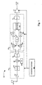
- FIG. 1 is a functional block diagram of one channel of a digital radio 100 embodying the principles of the present invention.
- Digital radio 100 includes an analog section or front-end 101 which receives radio frequency (RF) signals from an associated antenna 102.
- Analog front-end 101 is preferably a conventional RF down-converter including a low noise amplifier (LNA) 103 for setting the system noise figure, a bandpass filter 104 and mixer 105 driven by an analog local oscillator 106.
- LNA low noise amplifier
- mixer 105 driven by an analog local oscillator 106.
- the mixed-down analog signal is then converted into digital form by analog to digital converter 107.
- the digitized data output from A / D converter 107 is passed to digital processing section 108.
- a pair of mixers 109a,b generate in-phase (I) and quadrature (Q) signals from a corresponding pair of clock phases from crystal oscillator 110.
- the I and Q signals are next passed through bandpass filters 111a and 111b and on to digital baseband processor 112.
- the processed digital signal is then re-converted to analog (audio) form by D/A converter 113.
- a switched mode (Class D) audio power amplifier (APA) 114 is used to drive an external set of speakers or a headset.
- APA switched mode audio power amplifier
- SMPS switched mode power supply
- Power supply 115 will also be discussed further below.
- radio 100 is receiving a signal near one of the harmonics of the switching frequency, the switching frequency is moved such that the resulting switching noise will not interfere with received signal.
- a and B used in either APA 114 or SMPS 115, or both, have base frequencies of 350 kHz and 380 kHz, respectively. (More than two signals can be used to provide a greater resolution).
- the corresponding harmonics are then: A (kHz) B (kHz) 700 760 1050 1140 1400 1520
- One of the signals A and B is then selected as a function of the frequency of the received signal.
- the selection could be made as follows: Receive Freq. (kHz) Switching Signal Under 730 B 930 -910 A 910 - 1100 B 1110 - 1280 A 1290 - 1460 B Above 1460 A
- the interference created by the switching signal and its harmonics are moved above or below the reception band, where their effect on noise performance is minimized.
- the selection of the reception band is performed by a microcontroller or microprocessor which can accordingly also instruct the PWM control circuitry to change frequency.
- the PWM control circuitry can count the frequency of the local oscillator and choose the PWM frequency accordingly.
- the different switching frequencies can be generated by frequency division.
- FIGURE 2 is a simplified functional block diagram of a Class D pulse width modulated (PWM) amplifier 200 suitable for use as APA 114 in one channel of system 100.
- PWM pulse width modulated
- the gates/drivers 202a,b are controlled by a PWM modulated signal generated by digital PWM controller 204 which receives the analog audio signal Audio In, along with a high speed clock and a lower frequency clock, discussed below.
- PWM controller 204 also receives feedback from the outputs of the MOSFET pairs.
- PWM signal generation techniques are discussed in coassigned U.S. Patent No. 5,815,102 to Melanson , entitled “Delta Sigma PWM DAC to Reduce Switching". The result is a PWM signal having pulse widths proportional to the input signal amplitude.
- a low pass filter 203 is used to recover the amplified audio input signal.
- the frequency of low frequency clock (square wave) can be adjusted, as described above, such that the PWM switching signal driving the output MOSFETs (through gates /drivers 202) is shifted out of the reception band.
- a programmable frequency divider 209 is used to generate multiple clock frequencies for driving ramp generator 205.
- Divider 209 could for example start with a base frequency of 512 fs, where fs is the sampling frequency used in the A/D conversion process, and divide by 64 to obtain a frequency of 8 fs.
- the resulting 64 time slots make it possible to generate PWM pulse widths from 0 to 64 periods wide. Similar, if the divide ratio is changed, for example, to 72, then 72 time slots are available modifying the switching frequency in the ratio of 8:9.
- divider 209 is programmable with the divide ratio selected by microcontroller 208 as a function of the received frequency.
- Switched mode power supplies such as SMPS 115 in system 100.
- a simplified functional diagram of a switched mode power supply 300 is shown in FIGURE 3 for purposes of illustrating the inventive concepts. It should be noted that while the illustrated embodiment employs an analog ramp generator and analog comparator, that a digital PWM controller similar to that discussed above can also be instead used in SMPS 115.
- SMPS 300 is based on a power MOSFET or semiconductor switch 301 driving an inductor 302 and output impedance 303.
- Inductor (core) 302 generally filters current ripple while a capacitor 304 is included for filtering voltage ripple.
- Free-wheeling diode 305 ensures that current is always flowing into inductor 302.
- a feedback loop is represented by differential error amplifier 306 which compares a feedback signal from the circuit output against a reference voltage Vref.
- SWPS 300 also includes a crystal oscillator 309 controlled by a microcontroller 310.
- a programmable frequency divider 312 is used to generate multiple frequencies by dividing down a base frequency, as described above.
Landscapes
- Engineering & Computer Science (AREA)
- Power Engineering (AREA)
- Computer Networks & Wireless Communication (AREA)
- Signal Processing (AREA)
- Amplifiers (AREA)
- Noise Elimination (AREA)
- Networks Using Active Elements (AREA)
Claims (11)
- System (100) mit einem Funkempfänger (101, 108), das aufweist:einen Endtransistor (201);eine schaltende Schaltung (114, 200, 115, 300) mit einem digitalen Impulsbreitenmodulations-Schaltkreis (204) zum Erzeugen eines impulsbreitenmodulierten Signals einer ausgewählten Frequenz als Antwort auf ein analoges Eingangssignal und erste und zweite digitale Signale, die zueinander ein ausgewähltes Teilerverhältnis aufweisen, zum Schalten des Zustandes des Endtransistors; undeine Schaltung (207, 209, 311, 312) zum Einstellen der Frequenz des impulsbreitenmodulierten Signals als Funktion einer Frequenz eines von dem Funkempfänger empfangenen Signals, der umfasst:einen Signalerzeuger (206) zum Erzeugen des ersten digitalen Signals einer ausgewählten Grundfrequenz;einen Schaltkreis (209) zum Teilen der Grundfrequenz des ersten digitalen Signals durch einen ausgewählten Divisor, um das zweite digitale Signal bei der Frequenz des impulsbreitenmodulierten Signals zur Verwendung durch die schaltende Schaltung zu erzeugen; undeinen Schaltkreis (208) zum Auswählen des Divisors als Funktion der Frequenz des von dem Funkempfänger empfangenen Signals, um unterschiedliche Verhältnisse zwischen den ersten und zweiten digitalen Signalen für vom Funkempfänger empfangene Signale unterschiedliche Frequenzen bereitzustellen.
- System nach Anspruch 1, bei welchem die schaltende Schaltung eine schaltende Leistungsversorgung (115, 300) umfasst.
- System nach Anspruch 1, bei welchem die schaltende Schaltung einen Klasse-D-Verstärker (114, 200) umfasst.
- System nach Anspruch 1, bei welchem der Schaltkreis zum Auswählen des Divisors einen Mikrocontroller (208) umfasst, der so betreibbar ist, dass er die Frequenz des impulsbreitenmodulierten Signals auswählt, und zwar in Antwort auf die Auswahl eines Funkempfangsbandes, das seinerseits als Antwort auf eine Anwendereingabe ausgewählt wurde.
- System nach Anspruch 1, bei welchem der Signalerzeuger einen Quarzoszillator (206) umfasst.
- System nach Anspruch 1, bei welchem das impulsbreitenmodulierte Signal so ausgewählt wird, dass wenigstens eine Oberwelle des impulsbreitenmodulierten Signals außerhalb eines ausgewählten Frequenzbandes liegt, welches das vom Funkemfänger empfangene Signal umfasst.
- Schaltverfahren eines Transistors (201) in einem Funkempfänger (101, 108), das umfasst:Bestimmen einer Frequenz eines von dem Funkempfänger empfangenen Signals;digitales Erzeugen eines impulsbreitenmodulierten Signals zum Schalten des Transistors als Antwort auf das Bestimmen der Frequenz des empfangenen Signals, umfassend:Erzeugen eines digitalen Grundsignals mit einer ausgewählten Grundfrequenz;Teilen der Grundfrequenz durch einen ausgewählten Divisor, um ein weiteres digitales Signal mit der Frequenz des impulsbreitenmodulierten Signals zu erzeugen, wobei die Grundfrequenz und die Frequenz des weiteren digitalen Signals ein ausgewähltes Teilerverhältnis zueinander aufweisen;Auswählen des Divisors als Funktion der Frequenz des vom Funkempfänger empfangenen Signals, um unterschiedliche Teilerverhältnisse zwischen der Grundfrequenz und der Frequenz des weiteren digitalen Signals für unterschiedliche Frequenzen des vom Funkempfänger empfangenen Signals bereitzustellen; unddigitales Erzeugen des impulsbreitenmodulierten Signals in einem digitalen Impulsbreitenmodulator, der in Antwort auf das digitale Signal, das weitere digitale Signal und ein analoges Eingangssignal betrieben wird.
- Verfahren nach Anspruch 7, bei welchem das Erzeugen eines Grundsignals ein Erzeugen eines Grundsignals mit einem Quarzoszillator (206) umfasst.
- Verfahren nach Anspruch 7, bei welchem das digitales Erzeugen des impulsbreitenmodulierten Signals ein Erzeugen des impulsbreitenmodulierten Signals mit einem digitalen Impulsbreitenmodulationssteuergerät (204) umfasst.
- Verfahren nach Anspruch 7, bei welchem das Auswählen des Divisors ein Auswählen des Divisors mit einem Mikrocontroller (208) umfasst, der betreibar ist, die Frequenz des impulsbreitenmodulierten Signals in Antwort auf eine Auswahl eines Funkempfangsbandes in Antwort auf eine Anwendereingabe auszuwählen.
- Verfahren nach Anspruch 7, bei welchem das Auswählen des Divisors ein Auswählen des Divisors so umfasst, dass wenigstens eine Oberwelle des impulsbreitenmodulierten Signals außerhalb eines ausgewählten Frequenzbandes liegt, welches das vom Funkempfänger empfangene Signal umfasst.
Applications Claiming Priority (3)
| Application Number | Priority Date | Filing Date | Title |
|---|---|---|---|
| US65182100A | 2000-08-30 | 2000-08-30 | |
| US651821 | 2000-08-30 | ||
| PCT/US2001/041923 WO2002019551A2 (en) | 2000-08-30 | 2001-08-29 | Circuits and methods for reducing interference from switched mode circuits |
Publications (2)
| Publication Number | Publication Date |
|---|---|
| EP1314256A2 EP1314256A2 (de) | 2003-05-28 |
| EP1314256B1 true EP1314256B1 (de) | 2007-12-19 |
Family
ID=24614362
Family Applications (1)
| Application Number | Title | Priority Date | Filing Date |
|---|---|---|---|
| EP01964656A Expired - Lifetime EP1314256B1 (de) | 2000-08-30 | 2001-08-29 | Schaltungen und verfahren zur interferenz verminderung für schaltende schaltungen |
Country Status (9)
| Country | Link |
|---|---|
| US (2) | US7010271B2 (de) |
| EP (1) | EP1314256B1 (de) |
| JP (1) | JP2004507967A (de) |
| AT (1) | ATE381814T1 (de) |
| AU (1) | AU2001285491A1 (de) |
| DE (1) | DE60131989T2 (de) |
| DK (1) | DK1314256T3 (de) |
| TW (1) | TW519792B (de) |
| WO (1) | WO2002019551A2 (de) |
Families Citing this family (29)
| Publication number | Priority date | Publication date | Assignee | Title |
|---|---|---|---|---|
| US7212787B2 (en) * | 2001-11-29 | 2007-05-01 | Nasaco Electronics (Hong Kong) Ltd. | Wireless audio transmission system |
| JP2004048701A (ja) * | 2002-05-14 | 2004-02-12 | Sony Corp | オーディオ装置及びオーディオ装置の制御方法 |
| AU2003253191A1 (en) * | 2002-10-02 | 2004-04-23 | Koninklijke Philips Electronics N.V. | Circui and method for reducing interference from switched mode circuits |
| JP2005045549A (ja) * | 2003-07-22 | 2005-02-17 | Orion Denki Kk | 受信装置を備えた電気機器 |
| EP1687889B1 (de) * | 2003-11-14 | 2008-02-27 | Bobinados de Transformadores S.L. | Tuner-kompatible schaltnetzteilarchitektur |
| ATE340432T1 (de) * | 2003-12-29 | 2006-10-15 | Freescale Semiconductor Inc | Niedrigzwischenfrequenzempfänger |
| KR100638472B1 (ko) * | 2004-11-08 | 2006-10-26 | 삼성전자주식회사 | 디지털 오디오 증폭기, 그것을 포함하는 오디오 시스템,및 오디오 신호 증폭방법 |
| JP2006173819A (ja) * | 2004-12-14 | 2006-06-29 | Sharp Corp | スイッチングアンプ |
| US7474893B2 (en) * | 2004-12-29 | 2009-01-06 | Silicon Laboratories, Inc. | System including a communication apparatus having a digital audio interface for audio testing with radio isolation |
| US7676197B2 (en) * | 2005-06-30 | 2010-03-09 | Intel Corporation | Signal spectrum steering method, apparatus, and system |
| US7528586B2 (en) * | 2005-12-21 | 2009-05-05 | Honeywell International Inc. | Harmonics related synchronization for switching regulators |
| US7649410B2 (en) * | 2006-01-24 | 2010-01-19 | D2Audio Corporation | Systems and methods for improving performance in a digital amplifier by adding an ultrasonic signal to an input audio signal |
| FI20065457A0 (fi) * | 2006-06-30 | 2006-06-30 | Nokia Corp | Tehovahvistimen kytkentätoimisen tehonsyötön kontrollointi |
| EP2263355B1 (de) * | 2008-03-31 | 2012-09-12 | Nxp B.V. | Hochauflösender digitaler Modulator mit Umschaltung zwischen diskreten PWM- und PPM-Werten |
| WO2010044017A1 (en) * | 2008-10-13 | 2010-04-22 | Koninklijke Philips Electronics N.V. | Switching power supply. |
| US8294445B2 (en) * | 2008-12-04 | 2012-10-23 | Qualcomm Incorporated | Switching voltage regulator with frequency selection |
| JP5202354B2 (ja) * | 2009-01-22 | 2013-06-05 | キヤノン株式会社 | D級増幅装置 |
| US8265303B2 (en) * | 2009-03-11 | 2012-09-11 | Pacifictech Microelectronics, Inc. | Circuits and methods for reducing pop noise in class D amplifiers |
| TWI380580B (en) * | 2009-08-20 | 2012-12-21 | Richtek Technology Corp | Variable frequency class-d amplifier and a control method thereof and a ramp generator for the variable freguency class-d amplifier and a method thereof |
| US8391512B2 (en) | 2009-09-25 | 2013-03-05 | Onkyo Corporation | Broadcast wave receiving system |
| US8145149B2 (en) * | 2010-06-17 | 2012-03-27 | R2 Semiconductor, Inc | Operating a voltage regulator at a switching frequency selected to reduce spurious signals |
| FR2978313B1 (fr) * | 2011-07-18 | 2014-02-21 | Thales Sa | Procede pour preserver la sensibilite d'un equipement radiofrequence et equipement radiofrequence |
| JP6024175B2 (ja) * | 2012-04-18 | 2016-11-09 | 富士電機株式会社 | スイッチング電源装置 |
| EP2712077A1 (de) * | 2012-09-20 | 2014-03-26 | Alcatel-Lucent | Modulation |
| JP6089974B2 (ja) * | 2013-05-30 | 2017-03-08 | 株式会社デンソー | 電力線通信システム、マスタ及びスレーブ |
| TWI511426B (zh) * | 2013-08-30 | 2015-12-01 | Anpec Electronics Corp | 調變方法及其調變模組與電壓轉換裝置 |
| US9837958B2 (en) * | 2015-06-08 | 2017-12-05 | Maxlinear, Inc. | Crystal (xtal) oscillator with high interference immunity |
| JP6675888B2 (ja) * | 2016-03-07 | 2020-04-08 | エイブリック株式会社 | デジタル無線送信装置 |
| JP7067259B2 (ja) * | 2018-05-18 | 2022-05-16 | 株式会社デンソー | インバータ制御システム |
Family Cites Families (31)
| Publication number | Priority date | Publication date | Assignee | Title |
|---|---|---|---|---|
| US4048561A (en) | 1975-11-28 | 1977-09-13 | Robyn International, Inc. | Apparatus for preventing simultaneous transmission and channel selection in a transmitter or transceiver |
| US4188585A (en) | 1978-03-16 | 1980-02-12 | Cincinnati Electronics Corporation | Synchronized receiver power system |
| JPS6052607B2 (ja) * | 1979-05-10 | 1985-11-20 | ヤマハ株式会社 | 増幅器 |
| US4233685A (en) * | 1979-11-23 | 1980-11-11 | Ford Motor Company | Radio for receiving and reproducing information broadcast on the intermediate frequency |
| NZ211797A (en) | 1984-04-17 | 1989-08-29 | South Australia Electr Trust | Ripple control: receiver with synchronous filter outputs squared and summed |
| GB2170663B (en) | 1985-02-02 | 1989-06-14 | Brian Ernest Attwood | Harmonic-resonant power supply |
| JPH0785524B2 (ja) * | 1988-12-28 | 1995-09-13 | パイオニア株式会社 | パルス幅変調増幅回路 |
| US5072171A (en) | 1990-01-23 | 1991-12-10 | Hughes Aircraft Company | High efficiency power converter employing a synchronized switching system |
| US5043857A (en) | 1990-04-11 | 1991-08-27 | Sundstrand Corporation | Real-time control of PWM inverters by pattern development from stored constants |
| TW304316B (de) * | 1990-10-03 | 1997-05-01 | Yamaha Corp | |
| GB9103777D0 (en) * | 1991-02-22 | 1991-04-10 | B & W Loudspeakers | Analogue and digital convertors |
| DE59209190D1 (de) * | 1991-11-01 | 1998-03-12 | Thomson Consumer Electronics | Rundfunkübertragungssystem und rundfunkempfänger |
| US5275715A (en) * | 1992-01-23 | 1994-01-04 | Micron Technology Inc. | Electroplating process for enhancing the conformality of titanium and titanium nitride films in the manufacture of integrated circuits and structures produced thereby |
| US5471663A (en) | 1993-07-01 | 1995-11-28 | Motorola, Inc. | Expanded microcomputer system for controlling radio frequency interference |
| US5387913A (en) * | 1993-11-09 | 1995-02-07 | Motorola, Inc. | Receiver with digital tuning and method therefor |
| US5537305A (en) * | 1994-10-11 | 1996-07-16 | Telephonics Corporation | Synchronously tuned power converter method and apparatus |
| US5765113A (en) | 1994-12-29 | 1998-06-09 | Russo; David William | Method and apparatus for avoiding desensitization of a radio frequency receiver |
| US5907482A (en) | 1995-11-30 | 1999-05-25 | Toko, Inc. | Power supply control device |
| GB2314474B (en) | 1996-06-21 | 2001-03-07 | Univ Bristol | Low power audio device |
| JP3570846B2 (ja) | 1997-03-27 | 2004-09-29 | Necアクセステクニカ株式会社 | 無線携帯情報端末 |
| KR100240328B1 (ko) * | 1997-04-30 | 2000-01-15 | 전주범 | Dvcr의 오디오 재생 클럭 발생 장치 |
| US5959501A (en) * | 1998-01-14 | 1999-09-28 | Harris Corporation | Class D amplifier with scaled clock and related methods |
| US5959815A (en) * | 1998-03-17 | 1999-09-28 | Gateway 2000, Inc. | Method and apparatus for detecting potentially damaging electrical fields |
| JPH11332230A (ja) * | 1998-05-07 | 1999-11-30 | Alinco Inc | スイッチング電源 |
| WO2000007291A2 (en) | 1998-07-24 | 2000-02-10 | Toccata Technology Aps | A method of attenuating zero crossing distortion and noise in an amplifier, an amplifier and uses of the method and the amplifier |
| US6304594B1 (en) | 1998-07-27 | 2001-10-16 | General Dynamics Government Systems Corporation | Interference detection and avoidance technique |
| US6107875A (en) * | 1998-10-15 | 2000-08-22 | Intersil Corporation | Variable frequency class D modulator with built in soft clipping and frequency limiting |
| US6587670B1 (en) * | 1998-12-22 | 2003-07-01 | Harris Corporation | Dual mode class D amplifiers |
| US6344811B1 (en) * | 1999-03-16 | 2002-02-05 | Audio Logic, Inc. | Power supply compensation for noise shaped, digital amplifiers |
| US6563893B2 (en) * | 2001-05-17 | 2003-05-13 | Ut-Battelle, Llc | Carrier-frequency synchronization system for improved amplitude modulation and television broadcast reception |
| US6965335B1 (en) * | 2003-09-15 | 2005-11-15 | Cirrus Logic, Inc. | Methods for output edge-balancing in pulse width modulation systems and data converters using the same |
-
2001
- 2001-08-27 TW TW090121055A patent/TW519792B/zh not_active IP Right Cessation
- 2001-08-29 AU AU2001285491A patent/AU2001285491A1/en not_active Abandoned
- 2001-08-29 AT AT01964656T patent/ATE381814T1/de not_active IP Right Cessation
- 2001-08-29 WO PCT/US2001/041923 patent/WO2002019551A2/en not_active Ceased
- 2001-08-29 JP JP2002523734A patent/JP2004507967A/ja active Pending
- 2001-08-29 DK DK01964656T patent/DK1314256T3/da active
- 2001-08-29 DE DE60131989T patent/DE60131989T2/de not_active Expired - Lifetime
- 2001-08-29 EP EP01964656A patent/EP1314256B1/de not_active Expired - Lifetime
-
2003
- 2003-11-18 US US10/715,950 patent/US7010271B2/en not_active Expired - Lifetime
-
2005
- 2005-10-26 US US11/258,668 patent/US7199744B1/en not_active Expired - Lifetime
Also Published As
| Publication number | Publication date |
|---|---|
| WO2002019551A3 (en) | 2002-08-15 |
| EP1314256A2 (de) | 2003-05-28 |
| ATE381814T1 (de) | 2008-01-15 |
| WO2002019551A2 (en) | 2002-03-07 |
| US20040100328A1 (en) | 2004-05-27 |
| DE60131989D1 (de) | 2008-01-31 |
| TW519792B (en) | 2003-02-01 |
| US7010271B2 (en) | 2006-03-07 |
| DE60131989T2 (de) | 2008-12-11 |
| US7199744B1 (en) | 2007-04-03 |
| DK1314256T3 (da) | 2008-05-05 |
| AU2001285491A1 (en) | 2002-03-13 |
| JP2004507967A (ja) | 2004-03-11 |
Similar Documents
| Publication | Publication Date | Title |
|---|---|---|
| EP1314256B1 (de) | Schaltungen und verfahren zur interferenz verminderung für schaltende schaltungen | |
| US6768376B2 (en) | Dual mode class D amplifiers | |
| EP1130770B1 (de) | Funknetzwerk mit geringer Leistung | |
| TWI427913B (zh) | 功率轉換器的振盪信號頻率之動態選擇 | |
| US7319763B2 (en) | Power amplification for parametric loudspeakers | |
| EP1320927B1 (de) | Leistungsverstärkung für parametrische lautsprecher | |
| US8520785B2 (en) | Multimode receiver with a translational loop for input matching | |
| Abidi | CMOS wireless transceivers: The new wave | |
| US6680657B2 (en) | Cross-coupled voltage controlled oscillator with improved phase noise performance | |
| US6510314B1 (en) | Mixer circuit with output stage for implementation on integrated circuit | |
| US7142819B1 (en) | Circuits and methods for controlling switching noise in switched-mode circuits | |
| WO1999034505A1 (en) | A mixer for a receiver | |
| KR20040099283A (ko) | 무선 주파수 신호의 다운 컨버전을 위한 방법 및 장치 | |
| US6628166B2 (en) | RF communication system using an RF digital amplifier | |
| Song et al. | A 0.25-/spl mu/m CMOS quad-band GSM RF transceiver using an efficient LO frequency plan | |
| JP3712787B2 (ja) | Fm受信機 | |
| JP2000082779A (ja) | 受信機 | |
| KR20060109898A (ko) | 튜너 호환성이 있는 스위치 모드 전원 장치 아키텍처 | |
| JP2000082958A (ja) | 通信装置 | |
| JPS5839267A (ja) | パルススイツチング機器のラジオ雑音防止方法 | |
| WO2005104382A1 (ja) | 受信機 | |
| JP2001339299A (ja) | 発振信号生成器及び通信装置 |
Legal Events
| Date | Code | Title | Description |
|---|---|---|---|
| PUAI | Public reference made under article 153(3) epc to a published international application that has entered the european phase |
Free format text: ORIGINAL CODE: 0009012 |
|
| 17P | Request for examination filed |
Effective date: 20030207 |
|
| AK | Designated contracting states |
Designated state(s): AT BE CH CY DE DK ES FI FR GB GR IE IT LI LU MC NL PT SE TR |
|
| AX | Request for extension of the european patent |
Extension state: AL LT LV MK RO SI |
|
| RIN1 | Information on inventor provided before grant (corrected) |
Inventor name: MELANSON, JOHN, LAURENCE |
|
| 17Q | First examination report despatched |
Effective date: 20051018 |
|
| GRAP | Despatch of communication of intention to grant a patent |
Free format text: ORIGINAL CODE: EPIDOSNIGR1 |
|
| GRAS | Grant fee paid |
Free format text: ORIGINAL CODE: EPIDOSNIGR3 |
|
| GRAA | (expected) grant |
Free format text: ORIGINAL CODE: 0009210 |
|
| AK | Designated contracting states |
Kind code of ref document: B1 Designated state(s): AT BE CH CY DE DK ES FI FR GB GR IE IT LI LU MC NL PT SE TR |
|
| REG | Reference to a national code |
Ref country code: GB Ref legal event code: FG4D |
|
| REG | Reference to a national code |
Ref country code: IE Ref legal event code: FG4D |
|
| REG | Reference to a national code |
Ref country code: CH Ref legal event code: EP |
|
| REF | Corresponds to: |
Ref document number: 60131989 Country of ref document: DE Date of ref document: 20080131 Kind code of ref document: P |
|
| PG25 | Lapsed in a contracting state [announced via postgrant information from national office to epo] |
Ref country code: SE Free format text: LAPSE BECAUSE OF FAILURE TO SUBMIT A TRANSLATION OF THE DESCRIPTION OR TO PAY THE FEE WITHIN THE PRESCRIBED TIME-LIMIT Effective date: 20080319 Ref country code: LI Free format text: LAPSE BECAUSE OF FAILURE TO SUBMIT A TRANSLATION OF THE DESCRIPTION OR TO PAY THE FEE WITHIN THE PRESCRIBED TIME-LIMIT Effective date: 20071219 Ref country code: CH Free format text: LAPSE BECAUSE OF FAILURE TO SUBMIT A TRANSLATION OF THE DESCRIPTION OR TO PAY THE FEE WITHIN THE PRESCRIBED TIME-LIMIT Effective date: 20071219 |
|
| REG | Reference to a national code |
Ref country code: DK Ref legal event code: T3 |
|
| PG25 | Lapsed in a contracting state [announced via postgrant information from national office to epo] |
Ref country code: FI Free format text: LAPSE BECAUSE OF FAILURE TO SUBMIT A TRANSLATION OF THE DESCRIPTION OR TO PAY THE FEE WITHIN THE PRESCRIBED TIME-LIMIT Effective date: 20071219 |
|
| REG | Reference to a national code |
Ref country code: CH Ref legal event code: PL |
|
| PG25 | Lapsed in a contracting state [announced via postgrant information from national office to epo] |
Ref country code: AT Free format text: LAPSE BECAUSE OF FAILURE TO SUBMIT A TRANSLATION OF THE DESCRIPTION OR TO PAY THE FEE WITHIN THE PRESCRIBED TIME-LIMIT Effective date: 20071219 |
|
| PG25 | Lapsed in a contracting state [announced via postgrant information from national office to epo] |
Ref country code: ES Free format text: LAPSE BECAUSE OF FAILURE TO SUBMIT A TRANSLATION OF THE DESCRIPTION OR TO PAY THE FEE WITHIN THE PRESCRIBED TIME-LIMIT Effective date: 20080330 |
|
| PG25 | Lapsed in a contracting state [announced via postgrant information from national office to epo] |
Ref country code: BE Free format text: LAPSE BECAUSE OF FAILURE TO SUBMIT A TRANSLATION OF THE DESCRIPTION OR TO PAY THE FEE WITHIN THE PRESCRIBED TIME-LIMIT Effective date: 20071219 |
|
| PG25 | Lapsed in a contracting state [announced via postgrant information from national office to epo] |
Ref country code: PT Free format text: LAPSE BECAUSE OF FAILURE TO SUBMIT A TRANSLATION OF THE DESCRIPTION OR TO PAY THE FEE WITHIN THE PRESCRIBED TIME-LIMIT Effective date: 20080519 |
|
| EN | Fr: translation not filed | ||
| PLBE | No opposition filed within time limit |
Free format text: ORIGINAL CODE: 0009261 |
|
| STAA | Information on the status of an ep patent application or granted ep patent |
Free format text: STATUS: NO OPPOSITION FILED WITHIN TIME LIMIT |
|
| 26N | No opposition filed |
Effective date: 20080922 |
|
| PG25 | Lapsed in a contracting state [announced via postgrant information from national office to epo] |
Ref country code: GR Free format text: LAPSE BECAUSE OF FAILURE TO SUBMIT A TRANSLATION OF THE DESCRIPTION OR TO PAY THE FEE WITHIN THE PRESCRIBED TIME-LIMIT Effective date: 20080320 |
|
| PG25 | Lapsed in a contracting state [announced via postgrant information from national office to epo] |
Ref country code: MC Free format text: LAPSE BECAUSE OF NON-PAYMENT OF DUE FEES Effective date: 20080831 |
|
| PG25 | Lapsed in a contracting state [announced via postgrant information from national office to epo] |
Ref country code: FR Free format text: LAPSE BECAUSE OF FAILURE TO SUBMIT A TRANSLATION OF THE DESCRIPTION OR TO PAY THE FEE WITHIN THE PRESCRIBED TIME-LIMIT Effective date: 20081010 |
|
| PG25 | Lapsed in a contracting state [announced via postgrant information from national office to epo] |
Ref country code: IE Free format text: LAPSE BECAUSE OF NON-PAYMENT OF DUE FEES Effective date: 20080829 Ref country code: CY Free format text: LAPSE BECAUSE OF FAILURE TO SUBMIT A TRANSLATION OF THE DESCRIPTION OR TO PAY THE FEE WITHIN THE PRESCRIBED TIME-LIMIT Effective date: 20071219 |
|
| PG25 | Lapsed in a contracting state [announced via postgrant information from national office to epo] |
Ref country code: LU Free format text: LAPSE BECAUSE OF NON-PAYMENT OF DUE FEES Effective date: 20080829 |
|
| PG25 | Lapsed in a contracting state [announced via postgrant information from national office to epo] |
Ref country code: TR Free format text: LAPSE BECAUSE OF FAILURE TO SUBMIT A TRANSLATION OF THE DESCRIPTION OR TO PAY THE FEE WITHIN THE PRESCRIBED TIME-LIMIT Effective date: 20071219 |
|
| PG25 | Lapsed in a contracting state [announced via postgrant information from national office to epo] |
Ref country code: IT Free format text: LAPSE BECAUSE OF NON-PAYMENT OF DUE FEES Effective date: 20080831 |
|
| PGFP | Annual fee paid to national office [announced via postgrant information from national office to epo] |
Ref country code: NL Payment date: 20200826 Year of fee payment: 20 |
|
| PGFP | Annual fee paid to national office [announced via postgrant information from national office to epo] |
Ref country code: GB Payment date: 20200827 Year of fee payment: 20 Ref country code: DK Payment date: 20200827 Year of fee payment: 20 Ref country code: DE Payment date: 20200827 Year of fee payment: 20 |
|
| REG | Reference to a national code |
Ref country code: DE Ref legal event code: R071 Ref document number: 60131989 Country of ref document: DE |
|
| REG | Reference to a national code |
Ref country code: DK Ref legal event code: EUP Expiry date: 20210829 |
|
| REG | Reference to a national code |
Ref country code: NL Ref legal event code: MK Effective date: 20210828 |
|
| REG | Reference to a national code |
Ref country code: GB Ref legal event code: PE20 Expiry date: 20210828 |
|
| PG25 | Lapsed in a contracting state [announced via postgrant information from national office to epo] |
Ref country code: GB Free format text: LAPSE BECAUSE OF EXPIRATION OF PROTECTION Effective date: 20210828 |