EP1314969B1 - Detecteur optique - Google Patents
Detecteur optique Download PDFInfo
- Publication number
- EP1314969B1 EP1314969B1 EP01954435A EP01954435A EP1314969B1 EP 1314969 B1 EP1314969 B1 EP 1314969B1 EP 01954435 A EP01954435 A EP 01954435A EP 01954435 A EP01954435 A EP 01954435A EP 1314969 B1 EP1314969 B1 EP 1314969B1
- Authority
- EP
- European Patent Office
- Prior art keywords
- circuit
- output
- charges
- light detection
- capacitance
- Prior art date
- Legal status (The legal status is an assumption and is not a legal conclusion. Google has not performed a legal analysis and makes no representation as to the accuracy of the status listed.)
- Expired - Lifetime
Links
- 230000003287 optical effect Effects 0.000 title 1
- 239000003990 capacitor Substances 0.000 claims description 159
- 238000001514 detection method Methods 0.000 claims description 101
- 238000006243 chemical reaction Methods 0.000 claims description 48
- 238000009825 accumulation Methods 0.000 claims description 4
- 238000010586 diagram Methods 0.000 description 16
- 238000003384 imaging method Methods 0.000 description 5
- 230000035945 sensitivity Effects 0.000 description 5
- 230000010354 integration Effects 0.000 description 4
- 238000000034 method Methods 0.000 description 4
- 229920006395 saturated elastomer Polymers 0.000 description 2
- 230000003292 diminished effect Effects 0.000 description 1
- 238000004519 manufacturing process Methods 0.000 description 1
- 238000004886 process control Methods 0.000 description 1
- 238000013139 quantization Methods 0.000 description 1
Images


Classifications
-
- G—PHYSICS
- G01—MEASURING; TESTING
- G01J—MEASUREMENT OF INTENSITY, VELOCITY, SPECTRAL CONTENT, POLARISATION, PHASE OR PULSE CHARACTERISTICS OF INFRARED, VISIBLE OR ULTRAVIOLET LIGHT; COLORIMETRY; RADIATION PYROMETRY
- G01J1/00—Photometry, e.g. photographic exposure meter
- G01J1/42—Photometry, e.g. photographic exposure meter using electric radiation detectors
- G01J1/44—Electric circuits
- G01J1/46—Electric circuits using a capacitor
-
- H—ELECTRICITY
- H04—ELECTRIC COMMUNICATION TECHNIQUE
- H04N—PICTORIAL COMMUNICATION, e.g. TELEVISION
- H04N25/00—Circuitry of solid-state image sensors [SSIS]; Control thereof
- H04N25/70—SSIS architectures; Circuits associated therewith
- H04N25/76—Addressed sensors, e.g. MOS or CMOS sensors
- H04N25/78—Readout circuits for addressed sensors, e.g. output amplifiers or A/D converters
Definitions
- the light detection apparatus may further include an A/D converter circuit for converting into a digital signal a voltage (analog signal) output by the integrating circuit.
- the intensity of the incident light can be obtained as a digital value, and canbeprocessedbya computer and the like.
- the light detection apparatus can be employed as a solid-state image pickup apparatus.
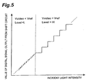
- the CMOS technique can be used to manufacture such a light detection apparatus, and when in the integrating circuit the capacitance of a capacitor for converting a current into a voltage is changed, the dynamic range for the detection of the intensity of the incident light can be increased.
- the capacitance of the integrating capacitor unit when the capacitance of the integrating capacitor unit is reduced, the detection sensitivity is increased, even when the intensity of the incident light is low. Meanwhile, when the capacitance of the integrating capacitor unit is increased, saturation of an output signal can be avoided, even when the intensity of the incident light is high.
- Cv in Fig. 1 is a capacitor provided to the wiring connected to the input end of the integrating circuit 10.
- the selector 201 receives at the input terminal A logic level L, and receives at the input terminal B the least significant bit D 0 of an 8-bit digital signal output by the A/D converter circuit 40.
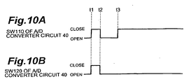
- the switch SW 13 in the integrating circuit 10 is once closed and is then opened.
- the capacitor Cf 11 integrates the amount (I sh ⁇ T int ) of charges generated, in consonance with the intensity of the incident light, by the photodiode PD, and the voltage V c output by the integrating circuit 10 is represented by the following equation (Fig. 4K).
- V c ( I sh ⁇ T int ) / C f 11
- the value of the digital signal output by the shift circuit 200 represents an excellent linearity relative to the intensity of the incident light.
- the level of a voltage output by the capacitance setting circuit 30 is changed at a predetermined value of the intensity of the incident light detected by the light detection device PD.
- the amount of charges to be integrated by the capacitor of the A/D converter circuit 40 at the succeeding stage is changed, and the resolution and the dynamic range of the A/D conversion are altered.
- the configuration employed for increasing the voltage applied at both ends of the capacitor is changed.
- the switches SW 110 and SW 120 are closed and then opened, and following t3, the switch SW 110 is closed to permit the use of the group of the sub-capacitors C S111 , C S112 , C S113 and C S114 , which have the base capacitance Cp. Since a large amount of charges can be integrated in the group of the sub-capacitors C S111 , C S112 , C S113 and C S114 , the A/D conversion can be performed with a wide dynamic range.
Landscapes
- Engineering & Computer Science (AREA)
- Power Engineering (AREA)
- Physics & Mathematics (AREA)
- General Physics & Mathematics (AREA)
- Spectroscopy & Molecular Physics (AREA)
- Multimedia (AREA)
- Signal Processing (AREA)
- Photometry And Measurement Of Optical Pulse Characteristics (AREA)
- Transforming Light Signals Into Electric Signals (AREA)
- Solid State Image Pick-Up Elements (AREA)
- Light Receiving Elements (AREA)
Claims (7)
- Dispositif de détection à ondes lumineuses comprenant :un circuit de détermination destiné à recevoir un signal analogique reflétant des charges en sortie du dispositif de détection à ondes lumineuses, et destiné à déterminer l'amplitude dudit signal analogique ;un circuit d'intégration, dans lequel un groupe de capacités connectées à l'étage arrière dudit dispositif de détection à ondes lumineuses est connecté en parallèle entre les bornes d'entrée/sortie d'un amplificateur opérationnel ; etun circuit de réglage de capacité destiné à régler, avant que ne démarre l'accumulation des charges dans ledit groupe de capacités, selon la sortie du circuit de détermination, une capacité combinée du groupe de capacités connectée entre les bornes d'entrée/sortie, de façon à définir une dynamique pour la tension de sortie dudit circuit d'intégration,dans lequel est exécutée une conversion A/N de ladite tension de sortie.
- Dispositif de détection à ondes lumineuses selon la revendication 1, comprenant en outre :un circuit de conversion A/N destiné à convertir la sortie dudit circuit d'intégration en un signal numérique.
- Dispositif de détection à ondes lumineuses selon la revendication 2, comprenant en outre :un circuit de décalage destiné à recevoir un signal de sortie numérique depuis ledit circuit de conversion A/N, et destiné à décaler les bits dudit signal numérique, selon la sortie dudit circuit de détermination, pour générer en sortie le signal résultant.
- Dispositif de détection à ondes lumineuses selon la revendication 2,
dans lequel ladite capacité combinée peut être réglée à une première capacité ou à une seconde capacité, et ladite première capacité est 2n fois (n étant un entier égal à, ou supérieur à, un) ladite seconde capacité, et
dans lequel ledit circuit de conversion A/N génère en sortie un signal numérique comportant n bits ou plus. - Dispositif de détection à ondes lumineuses comprenant :un circuit de détermination destiné à recevoir un signal analogique reflétant la sortie d'un dispositif de détection à ondes lumineuses, et destiné à déterminer l'amplitude dudit signal analogique ; etdes moyens de conversion A/N destinés à convertir ledit signal analogique en un signal numérique selon une résolution reflétant la sortie dudit circuit de détermination,dans lequel les moyens de conversion A/N comprennent
un circuit d'intégration connecté à l'étage arrière du dispositif de détection à ondes lumineuses, et
un circuit de conversion A/N, présentant
une capacité principale destinée à intégrer des charges proportionnelles à la sortie du circuit d'intégration,
des sous-capacités multiples destinées à intégrer lesdites charges qui sont transférées depuis la capacité principale dans laquelle lesdites charges ont été intégrées, et
un contrôleur de capacité destiné à commander le transfert desdites charges aux dites sous-capacités multiples, et destiné à générer en sortie la valeur de réglage sous la forme d'un signal numérique, et
dans lequel la proportion de charges cumulables dans chacune des sous-capacités est réglée selon la sortie dudit circuit de détermination. - Dispositif de détection à ondes lumineuses selon la revendication 5, dans lequel une tension appliquée aux deux extrémités de chacune desdites sous-capacités est déterminée selon la sortie dudit circuit de détermination, et la proportion des charges cumulables dans chacune desdites sous-capacités est réglée.
- Dispositif de détection à ondes lumineuses comprenant :un circuit de détermination destiné à recevoir un signal analogique reflétant la sortie d'un dispositif de détection à ondes lumineuses, et destiné à déterminer l'amplitude dudit signal analogique ; etdes moyens de conversion A/N destinés à convertir ledit signal analogique en un signal numérique selon une résolution reflétant la sortie dudit circuit de détermination,dans lequel les moyens de conversion A/N comprennent
un circuit d'intégration connecté à l'étage arrière dudit dispositif de détection à ondes lumineuses, et
un circuit de conversion A/N présentant
une capacité principale destinée à intégrer des charges proportionnelles à la sortie dudit circuit d'intégration,
des sous-capacités multiples destinées à intégrer lesdites charges qui sont transférées depuis ladite capacité principale, dans laquelle lesdites charges ont été intégrées, et
un contrôleur de capacité destiné à commander le transfert desdites charges aux dites sous-capacités multiples, et à générer en sortie la valeur de réglage sous la forme d'un signal numérique,
dans lequel un groupe de sous-capacités comportant un groupe spécifique de capacités est sélectionné dans lesdites sous-capacités multiples selon la sortie dudit circuit de détermination, et
dans lequel des charges sont transférées depuis ladite capacité principale vers ledit groupe sélectionné de sous-capacités sous le contrôle dudit contrôleur de capacité.
Applications Claiming Priority (3)
| Application Number | Priority Date | Filing Date | Title |
|---|---|---|---|
| JP2000235911 | 2000-08-03 | ||
| JP2000235911 | 2000-08-03 | ||
| PCT/JP2001/006699 WO2002012845A1 (fr) | 2000-08-03 | 2001-08-03 | Detecteur optique |
Publications (3)
| Publication Number | Publication Date |
|---|---|
| EP1314969A1 EP1314969A1 (fr) | 2003-05-28 |
| EP1314969A4 EP1314969A4 (fr) | 2005-07-20 |
| EP1314969B1 true EP1314969B1 (fr) | 2006-03-22 |
Family
ID=18728042
Family Applications (1)
| Application Number | Title | Priority Date | Filing Date |
|---|---|---|---|
| EP01954435A Expired - Lifetime EP1314969B1 (fr) | 2000-08-03 | 2001-08-03 | Detecteur optique |
Country Status (6)
| Country | Link |
|---|---|
| US (2) | US7286172B2 (fr) |
| EP (1) | EP1314969B1 (fr) |
| JP (1) | JP5197907B2 (fr) |
| AU (1) | AU2001276726A1 (fr) |
| DE (1) | DE60118202T2 (fr) |
| WO (1) | WO2002012845A1 (fr) |
Families Citing this family (19)
| Publication number | Priority date | Publication date | Assignee | Title |
|---|---|---|---|---|
| JP4414646B2 (ja) | 2002-11-18 | 2010-02-10 | 浜松ホトニクス株式会社 | 光検出装置 |
| JP2004200794A (ja) * | 2002-12-16 | 2004-07-15 | Hamamatsu Photonics Kk | 光検出装置 |
| JP4293588B2 (ja) * | 2002-12-16 | 2009-07-08 | 浜松ホトニクス株式会社 | 光検出装置 |
| JP3977735B2 (ja) | 2002-12-25 | 2007-09-19 | 浜松ホトニクス株式会社 | 光検出装置 |
| JP4663956B2 (ja) * | 2002-12-25 | 2011-04-06 | 浜松ホトニクス株式会社 | 光検出装置 |
| EP1628348A4 (fr) | 2003-05-23 | 2007-07-18 | Hamamatsu Photonics Kk | Dispositif de photodetection |
| JP4429785B2 (ja) * | 2004-04-19 | 2010-03-10 | 浜松ホトニクス株式会社 | 固体撮像装置 |
| JP4589030B2 (ja) * | 2004-05-10 | 2010-12-01 | 浜松ホトニクス株式会社 | 光検出装置 |
| US7605854B2 (en) * | 2004-08-11 | 2009-10-20 | Broadcom Corporation | Operational amplifier for an active pixel sensor |
| US7145188B2 (en) * | 2004-08-19 | 2006-12-05 | Broadcom Corporation | Apparatus and method of image processing to avoid image saturation |
| JP4744828B2 (ja) * | 2004-08-26 | 2011-08-10 | 浜松ホトニクス株式会社 | 光検出装置 |
| JP4314172B2 (ja) * | 2004-08-30 | 2009-08-12 | シャープ株式会社 | 増幅型固体撮像装置 |
| JP4931367B2 (ja) * | 2005-04-28 | 2012-05-16 | シャープ株式会社 | 検出装置及びそれを備えた表示装置 |
| US7561812B2 (en) * | 2005-10-13 | 2009-07-14 | Lite-On Technology Corp. | Optical receiver with matched photodetector capacitance |
| EP2005590B1 (fr) * | 2006-03-31 | 2011-06-15 | Nxp B.V. | Procede et systeme de pilote de signal a retroaction capacitive |
| JP5616025B2 (ja) * | 2009-01-22 | 2014-10-29 | 株式会社トプコン | 光波距離測定方法及び光波距離測定装置 |
| EP3685131B1 (fr) | 2017-09-19 | 2022-09-07 | Beckman Coulter, Inc. | Mesure de lumière analogique et comptage de photons dans des mesures de chimioluminescence |
| US12015427B2 (en) * | 2022-04-05 | 2024-06-18 | Stmicroelectronics (Research & Development) Limited | Photodiode current compatible input stage for a sigma-delta analog-to-digital converter |
| WO2025169558A1 (fr) * | 2024-02-05 | 2025-08-14 | コニカミノルタ株式会社 | Dispositif de mesure de lumière d'affichage, procédé de mesure de lumière et programme |
Family Cites Families (25)
| Publication number | Priority date | Publication date | Assignee | Title |
|---|---|---|---|---|
| US4764753A (en) * | 1984-07-23 | 1988-08-16 | Nec Corporation | Analog to digital converter |
| US4667179A (en) | 1985-03-07 | 1987-05-19 | Xerox Corporation | Two reference voltage weighted capacitor digital to analog converter |
| JPS63205527A (ja) | 1987-02-20 | 1988-08-25 | Sanyo Electric Co Ltd | 測光回路 |
| JPH0779243B2 (ja) | 1987-04-10 | 1995-08-23 | 日本電気株式会社 | オ−バ−サンプル形a/d変換器 |
| JPH02288709A (ja) * | 1989-04-28 | 1990-11-28 | Mitsubishi Electric Corp | 受光増幅器 |
| ES2035985T3 (es) | 1989-05-20 | 1993-05-01 | Hewlett-Packard Gmbh | Metodo de funcionamiento de un espectometro de fotodiodos y espectrometro de fotodiodos correspondiente. |
| JPH04110619A (ja) * | 1990-08-30 | 1992-04-13 | Topcon Corp | 測光用の装置 |
| US5030954A (en) | 1990-09-17 | 1991-07-09 | General Electric Company | Double rate oversampled interpolative modulators for analog-to-digital conversion |
| JPH0575464A (ja) | 1991-09-18 | 1993-03-26 | Nec Corp | A/d変換回路 |
| JPH05268097A (ja) | 1992-03-21 | 1993-10-15 | Hitachi Ltd | D/a変換器、及びオーバーサンプルa/d変換器 |
| JPH05291955A (ja) * | 1992-04-15 | 1993-11-05 | Nec Corp | Ad変換ビット伸長回路 |
| US5500645A (en) | 1994-03-14 | 1996-03-19 | General Electric Company | Analog-to-digital converters using multistage bandpass delta sigma modulators with arbitrary center frequency |
| JP3308146B2 (ja) * | 1995-06-02 | 2002-07-29 | 浜松ホトニクス株式会社 | 固体撮像装置 |
| JP3171091B2 (ja) | 1996-02-14 | 2001-05-28 | 日本電気株式会社 | 液晶画像信号制御方法及び制御回路 |
| US5892540A (en) * | 1996-06-13 | 1999-04-06 | Rockwell International Corporation | Low noise amplifier for passive pixel CMOS imager |
| JPH10153425A (ja) * | 1996-11-21 | 1998-06-09 | Inax Corp | 位置検出センサーの受光回路 |
| JP3628136B2 (ja) | 1997-01-30 | 2005-03-09 | 富士通株式会社 | 容量結合を利用した論理回路、ad変換回路及びda変換回路 |
| EP0901233B1 (fr) | 1997-09-05 | 2005-03-02 | STMicroelectronics S.r.l. | Modulateur du type sigma delta d'ordre deux à double échantillonnage présentant une architecture semi-bilinéaire |
| JP4098884B2 (ja) * | 1998-07-08 | 2008-06-11 | 浜松ホトニクス株式会社 | 固体撮像装置 |
| US6128039A (en) * | 1999-01-11 | 2000-10-03 | Omnivision Technologies, Inc. | Column amplifier for high fixed pattern noise reduction |
| EP1206131B1 (fr) * | 1999-08-05 | 2005-12-07 | Hamamatsu Photonics K.K. | Dispositif d'imagerie a semi-conducteur et dispositif de telemetrie |
| JP4424796B2 (ja) * | 1999-11-18 | 2010-03-03 | 浜松ホトニクス株式会社 | 光検出装置 |
| US6473122B1 (en) * | 1999-12-06 | 2002-10-29 | Hemanth G. Kanekal | Method and apparatus to capture high resolution images using low resolution sensors and optical spatial image sampling |
| JP4579433B2 (ja) * | 2001-02-27 | 2010-11-10 | 浜松ホトニクス株式会社 | A/d変換回路および固体撮像装置 |
| US6593562B1 (en) * | 2001-10-04 | 2003-07-15 | Indigo Systems Corporation | Electro-optical sensor arrays with reduced sensitivity to defects |
-
2001
- 2001-08-03 EP EP01954435A patent/EP1314969B1/fr not_active Expired - Lifetime
- 2001-08-03 WO PCT/JP2001/006699 patent/WO2002012845A1/fr not_active Ceased
- 2001-08-03 DE DE60118202T patent/DE60118202T2/de not_active Expired - Lifetime
- 2001-08-03 JP JP2002517479A patent/JP5197907B2/ja not_active Expired - Fee Related
- 2001-08-03 US US10/343,427 patent/US7286172B2/en not_active Expired - Lifetime
- 2001-08-03 AU AU2001276726A patent/AU2001276726A1/en not_active Abandoned
-
2007
- 2007-09-17 US US11/898,857 patent/US7969491B2/en not_active Expired - Fee Related
Also Published As
| Publication number | Publication date |
|---|---|
| US20080012974A1 (en) | 2008-01-17 |
| EP1314969A1 (fr) | 2003-05-28 |
| DE60118202D1 (de) | 2006-05-11 |
| DE60118202T2 (de) | 2007-04-12 |
| US7286172B2 (en) | 2007-10-23 |
| US20030156211A1 (en) | 2003-08-21 |
| US7969491B2 (en) | 2011-06-28 |
| JP5197907B2 (ja) | 2013-05-15 |
| EP1314969A4 (fr) | 2005-07-20 |
| WO2002012845A1 (fr) | 2002-02-14 |
| AU2001276726A1 (en) | 2002-02-18 |
Similar Documents
| Publication | Publication Date | Title |
|---|---|---|
| US7969491B2 (en) | Light detection apparatus | |
| US8063965B2 (en) | Apparatus and method for eliminating artifacts in active pixel sensor (APS) imagers | |
| US7218260B2 (en) | Column analog-to-digital converter of a CMOS image sensor for preventing a sun black effect | |
| JPWO2002012845A1 (ja) | 光検出装置 | |
| EP1197735B1 (fr) | Photodetecteur | |
| JP4440680B2 (ja) | 光検出装置 | |
| US20020113887A1 (en) | CMOS image sensor with extended dynamic range | |
| JP4589030B2 (ja) | 光検出装置 | |
| US11412169B2 (en) | Pixel circuit outputting over exposure information and method of calculating real intensity thereof, pixel array having the same | |
| GB2432065A (en) | Image sensor with comparator and logarithmic output | |
| EP1330037A1 (fr) | Convertisseur a/n et camera a semi-conducteur | |
| US6088057A (en) | Image pickup apparatus with reduced signal noise | |
| EP1136798A1 (fr) | Photodetecteur | |
| JP3091084B2 (ja) | 信号処理回路 | |
| US7718945B2 (en) | Solid state imaging device including photodetecting section, row selecting section for changing the electric charge accumulating time of each row, and signal processing section | |
| US7956917B2 (en) | Sensor apparatus | |
| US12452560B2 (en) | Image sensor including analog-to-digital converter and ramp voltage generator | |
| JP2002340670A (ja) | 光検出装置 |
Legal Events
| Date | Code | Title | Description |
|---|---|---|---|
| PUAI | Public reference made under article 153(3) epc to a published international application that has entered the european phase |
Free format text: ORIGINAL CODE: 0009012 |
|
| 17P | Request for examination filed |
Effective date: 20030226 |
|
| AK | Designated contracting states |
Designated state(s): AT BE CH CY DE DK ES FI FR GB GR IE IT LI LU MC NL PT SE TR |
|
| AX | Request for extension of the european patent |
Extension state: AL LT LV MK RO SI |
|
| RBV | Designated contracting states (corrected) |
Designated state(s): DE FR GB IT NL |
|
| A4 | Supplementary search report drawn up and despatched |
Effective date: 20050608 |
|
| RIC1 | Information provided on ipc code assigned before grant |
Ipc: 7G 01J 1/44 A Ipc: 7H 04N 5/335 B Ipc: 7G 01J 1/46 B |
|
| GRAP | Despatch of communication of intention to grant a patent |
Free format text: ORIGINAL CODE: EPIDOSNIGR1 |
|
| GRAS | Grant fee paid |
Free format text: ORIGINAL CODE: EPIDOSNIGR3 |
|
| GRAA | (expected) grant |
Free format text: ORIGINAL CODE: 0009210 |
|
| AK | Designated contracting states |
Kind code of ref document: B1 Designated state(s): DE FR GB IT NL |
|
| REG | Reference to a national code |
Ref country code: GB Ref legal event code: FG4D |
|
| REF | Corresponds to: |
Ref document number: 60118202 Country of ref document: DE Date of ref document: 20060511 Kind code of ref document: P |
|
| ET | Fr: translation filed | ||
| PLBE | No opposition filed within time limit |
Free format text: ORIGINAL CODE: 0009261 |
|
| STAA | Information on the status of an ep patent application or granted ep patent |
Free format text: STATUS: NO OPPOSITION FILED WITHIN TIME LIMIT |
|
| 26N | No opposition filed |
Effective date: 20061227 |
|
| REG | Reference to a national code |
Ref country code: FR Ref legal event code: PLFP Year of fee payment: 16 |
|
| REG | Reference to a national code |
Ref country code: FR Ref legal event code: PLFP Year of fee payment: 17 |
|
| REG | Reference to a national code |
Ref country code: FR Ref legal event code: PLFP Year of fee payment: 18 |
|
| PGFP | Annual fee paid to national office [announced via postgrant information from national office to epo] |
Ref country code: IT Payment date: 20180823 Year of fee payment: 18 Ref country code: DE Payment date: 20180724 Year of fee payment: 18 Ref country code: FR Payment date: 20180712 Year of fee payment: 18 Ref country code: NL Payment date: 20180712 Year of fee payment: 18 |
|
| PGFP | Annual fee paid to national office [announced via postgrant information from national office to epo] |
Ref country code: GB Payment date: 20180801 Year of fee payment: 18 |
|
| REG | Reference to a national code |
Ref country code: DE Ref legal event code: R119 Ref document number: 60118202 Country of ref document: DE |
|
| REG | Reference to a national code |
Ref country code: NL Ref legal event code: MM Effective date: 20190901 |
|
| GBPC | Gb: european patent ceased through non-payment of renewal fee |
Effective date: 20190803 |
|
| PG25 | Lapsed in a contracting state [announced via postgrant information from national office to epo] |
Ref country code: NL Free format text: LAPSE BECAUSE OF NON-PAYMENT OF DUE FEES Effective date: 20190901 Ref country code: DE Free format text: LAPSE BECAUSE OF NON-PAYMENT OF DUE FEES Effective date: 20200303 Ref country code: FR Free format text: LAPSE BECAUSE OF NON-PAYMENT OF DUE FEES Effective date: 20190831 |
|
| PG25 | Lapsed in a contracting state [announced via postgrant information from national office to epo] |
Ref country code: GB Free format text: LAPSE BECAUSE OF NON-PAYMENT OF DUE FEES Effective date: 20190803 Ref country code: IT Free format text: LAPSE BECAUSE OF NON-PAYMENT OF DUE FEES Effective date: 20190803 |