EP1315247A2 - Elektrischer Steckverbinder mit Abdeck- und Ausrichtmitteln - Google Patents
Elektrischer Steckverbinder mit Abdeck- und Ausrichtmitteln Download PDFInfo
- Publication number
- EP1315247A2 EP1315247A2 EP02026234A EP02026234A EP1315247A2 EP 1315247 A2 EP1315247 A2 EP 1315247A2 EP 02026234 A EP02026234 A EP 02026234A EP 02026234 A EP02026234 A EP 02026234A EP 1315247 A2 EP1315247 A2 EP 1315247A2
- Authority
- EP
- European Patent Office
- Prior art keywords
- shutter plate
- housing
- mating
- connector
- electrical connector
- Prior art date
- Legal status (The legal status is an assumption and is not a legal conclusion. Google has not performed a legal analysis and makes no representation as to the accuracy of the status listed.)
- Withdrawn
Links
- 230000013011 mating Effects 0.000 claims abstract description 81
- 230000001681 protective effect Effects 0.000 claims abstract description 29
- 230000000295 complement effect Effects 0.000 claims description 10
- 230000014759 maintenance of location Effects 0.000 claims description 9
- 239000002184 metal Substances 0.000 claims description 6
- 239000007769 metal material Substances 0.000 description 2
- 238000003780 insertion Methods 0.000 description 1
- 230000037431 insertion Effects 0.000 description 1
- 239000000463 material Substances 0.000 description 1
- 238000000034 method Methods 0.000 description 1
Images


Classifications
-
- H—ELECTRICITY
- H01—ELECTRIC ELEMENTS
- H01R—ELECTRICALLY-CONDUCTIVE CONNECTIONS; STRUCTURAL ASSOCIATIONS OF A PLURALITY OF MUTUALLY-INSULATED ELECTRICAL CONNECTING ELEMENTS; COUPLING DEVICES; CURRENT COLLECTORS
- H01R13/00—Details of coupling devices of the kinds covered by groups H01R12/70 or H01R24/00 - H01R33/00
- H01R13/44—Means for preventing access to live contacts
- H01R13/447—Shutter or cover plate
- H01R13/453—Shutter or cover plate opened by engagement of counterpart
- H01R13/4538—Covers sliding or withdrawing in the direction of engagement
-
- H—ELECTRICITY
- H01—ELECTRIC ELEMENTS
- H01R—ELECTRICALLY-CONDUCTIVE CONNECTIONS; STRUCTURAL ASSOCIATIONS OF A PLURALITY OF MUTUALLY-INSULATED ELECTRICAL CONNECTING ELEMENTS; COUPLING DEVICES; CURRENT COLLECTORS
- H01R12/00—Structural associations of a plurality of mutually-insulated electrical connecting elements, specially adapted for printed circuits, e.g. printed circuit boards [PCB], flat or ribbon cables, or like generally planar structures, e.g. terminal strips, terminal blocks; Coupling devices specially adapted for printed circuits, flat or ribbon cables, or like generally planar structures; Terminals specially adapted for contact with, or insertion into, printed circuits, flat or ribbon cables, or like generally planar structures
- H01R12/70—Coupling devices
- H01R12/71—Coupling devices for rigid printing circuits or like structures
- H01R12/712—Coupling devices for rigid printing circuits or like structures co-operating with the surface of the printed circuit or with a coupling device exclusively provided on the surface of the printed circuit
- H01R12/716—Coupling device provided on the PCB
-
- H—ELECTRICITY
- H01—ELECTRIC ELEMENTS
- H01R—ELECTRICALLY-CONDUCTIVE CONNECTIONS; STRUCTURAL ASSOCIATIONS OF A PLURALITY OF MUTUALLY-INSULATED ELECTRICAL CONNECTING ELEMENTS; COUPLING DEVICES; CURRENT COLLECTORS
- H01R12/00—Structural associations of a plurality of mutually-insulated electrical connecting elements, specially adapted for printed circuits, e.g. printed circuit boards [PCB], flat or ribbon cables, or like generally planar structures, e.g. terminal strips, terminal blocks; Coupling devices specially adapted for printed circuits, flat or ribbon cables, or like generally planar structures; Terminals specially adapted for contact with, or insertion into, printed circuits, flat or ribbon cables, or like generally planar structures
- H01R12/70—Coupling devices
- H01R12/71—Coupling devices for rigid printing circuits or like structures
- H01R12/72—Coupling devices for rigid printing circuits or like structures coupling with the edge of the rigid printed circuits or like structures
- H01R12/722—Coupling devices for rigid printing circuits or like structures coupling with the edge of the rigid printed circuits or like structures coupling devices mounted on the edge of the printed circuits
- H01R12/725—Coupling devices for rigid printing circuits or like structures coupling with the edge of the rigid printed circuits or like structures coupling devices mounted on the edge of the printed circuits containing contact members presenting a contact carrying strip, e.g. edge-like strip
-
- H—ELECTRICITY
- H01—ELECTRIC ELEMENTS
- H01R—ELECTRICALLY-CONDUCTIVE CONNECTIONS; STRUCTURAL ASSOCIATIONS OF A PLURALITY OF MUTUALLY-INSULATED ELECTRICAL CONNECTING ELEMENTS; COUPLING DEVICES; CURRENT COLLECTORS
- H01R12/00—Structural associations of a plurality of mutually-insulated electrical connecting elements, specially adapted for printed circuits, e.g. printed circuit boards [PCB], flat or ribbon cables, or like generally planar structures, e.g. terminal strips, terminal blocks; Coupling devices specially adapted for printed circuits, flat or ribbon cables, or like generally planar structures; Terminals specially adapted for contact with, or insertion into, printed circuits, flat or ribbon cables, or like generally planar structures
- H01R12/70—Coupling devices
- H01R12/82—Coupling devices connected with low or zero insertion force
- H01R12/85—Coupling devices connected with low or zero insertion force contact pressure producing means, contacts activated after insertion of printed circuits or like structures
- H01R12/88—Coupling devices connected with low or zero insertion force contact pressure producing means, contacts activated after insertion of printed circuits or like structures acting manually by rotating or pivoting connector housing parts
Definitions
- This invention generally relates to the art of electrical connectors and, more particularly, to an electrical connector which includes a movable shutter for protecting the terminals of the connector.
- a typical electrical connector includes a dielectric housing having a mating end to which a mating connector is connected, along with a plurality of terminals mounted on the housing.
- Each terminal typically includes a contact portion located generally at the mating end for engagement with appropriate contacts of the mating connector. If the connector is frequently connected with and disconnected from the mating connector, the contact portions of the terminals often are exposed exteriorly of the connector during the time the connector is disconnected. Therefore, the connector may be provided with some form of protective cover, slider or the like which acts as a shutter at the mating end for protecting the exposed contact portions of the terminals. Examples of such connectors are shown in Japanese Utility Model Laid-Open Nos. 5-1175 and 6-50270; and Japanese Patent Laid-Open Nos. 8-7973, 8-203594 and 9-63685.
- Such shutter members may be movably mounted so that they move out of a protective position when the connector is mated with the mating connector.
- movable shutters create considerable binding problems during such movement. This is particularly true when the connector, along with the shutter member, is considerably elongated in a direction transversely of the mating direction of the connector.
- the present invention is directed to solving these problems by yieldably mounting the shutter member to the connector housing to prevent binding of the shutter member upon movement relative to the housing.
- An object, therefore, of the invention is to provide a new and improved electrical connector of the character described, which includes a movable shutter member for protecting the terminals of the connector.
- the electrical connector includes a dielectric housing having a mating end for mating with a complementary mating connector.
- the mating end includes an upper wall and a pair of depending side walls at opposite sides of the upper wall defining an opening for receiving the mating connector.
- the housing is elongated between the side walls.
- a plurality of terminals are mounted on the housing in a side-by-side array longitudinally thereof. The terminals have contact portions exposed at the opening for engaging appropriate contacts of the mating connector.
- a shutter plate is movably mounted on the housing for movement from a protective position spanning the opening between the side walls for covering and protecting the contact portions of the terminals at the opening, to a retracted position upon mating of the mating connector to allow the contact portions of the terminals to engage the contacts of the mating connector.
- Complementary interengaging flexible locating means are provided between at least one side of the shutter plate and an adjacent one of the side walls of the housing to allow the shutter plate to yield relative to the housing and prevent binding of the shutter plate upon movement relative to the housing.
- one of the flexible locating means is provided between both opposite sides of the shutter plate and the pair of side walls of the housing.
- Biasing means in the form of a coil spring is provided between the shutter plate and the housing for biasing the shutter plate toward its protective position.
- the flexible locating means is provided by a spring member which, as disclosed herein, is a metal leaf spring.
- the flexible locating means includes retention means engageable with the shutter plate to define the protective position of the shutter plate. With the use of the leaf spring, a retention hook is provided on the leaf spring engageable with the shutter plate to define its protective position.
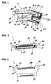
- Connector 10 for mating with a complementary mating connector, generally designated 12.
- Connector 10 includes a dielectric housing 14 mounting a plurality of terminals 16.
- the housing may be molded of plastic material, and the terminals may be stamped and formed from conductive sheet metal material.
- dielectric housing 16 includes a mating end 18 to which mating connector 12 is connected.
- a rear end 20 is opposite the mating end.
- the housing is elongated in a lateral or transverse direction perpendicular to the mating direction extending between mating end 18 and rear end 20.
- the housing has a pair of mounting bosses 22 at opposite sides thereof, generally flush with an upper surface 24 of the housing, for mounting the connector on a printed circuit board.
- a pair of mounting posts 26 are provided for insertion into appropriate mounting holes in the circuit board.
- Mating end 18 of housing 14 includes an upper wall 28 and a pair of downwardly depending side walls 30 at opposite sides of the upper wall.
- dielectric housing 14 is in the form of a plug which is open at the bottom side thereof, as at opening 32, for receiving portions of mating connector 12.
- Terminals 16 are mounted in respective terminal-receiving cavities 34 spaced laterally of the elongated housing, i.e., transversely of the mating direction of the connector. In other words, terminals 16 are mounted on the housing in a side-by-side array longitudinally of the housing.
- Each terminal includes a contact portion 36 which is bent downwardly into opening 32 at mating end 18 of the housing, a terminating portion 38 at rear end 20 of the housing and an intermediate portion 40 which is press-fit into a respective cavity 34 to fix the terminal within the housing.
- Terminal-receiving cavities 34 communicate with opening 32, and contact portions 36 of terminals 16 have contact ends 36a for engaging appropriate contacts of mating connector 12.
- Terminating portions 38 have tails 38a at rear end 20 of the housing generally flush with surface 24 for connection to appropriate circuit traces on the printed circuit board.
- Mating connector 12 mounts a plurality of terminals 40 for engaging contact ends 36a of contact portions 36 of terminals 16.
- the terminals are mounted on a dielectric housing portion 42 within a metal shell 44 of the mating connector.
- Housing 42 includes a plug portion 46 which moves into opening 32 of connector 10 when the connectors are mated.
- Mating connector 12 is mated with connector 10 at an angle as shown in Figure 1.
- a bottom edge of shell 44 abuts against housing 14 of connector 10, as at 50, whereupon mating connector 12 is rotated upwardly in the direction of arrow 52 as the top of the shell rides on a tapered upper surface 54 of housing 14 of connector 10.
- a clearance 56 (Fig. 1) is maintained between contact ends 36a of terminals 16 and terminals 40 of the mating connector to reduce the amount of mating forces.
- FIG. 8 shows mating connector 12 fully mated with connector 10.
- Mating connector 12 may be coupled to a portable information apparatus which includes a plug 58 (Fig. 8) having a circuit 60 insertable into a cavity 62 of housing 42, whereby the circuit engages contact portions 40a of terminals 40.
- the invention contemplates a shutter plate 60 which is positionable within a cavity 62 at the bottom of housing 14 of connector 10. This cavity communicates with opening 32 whereby the shutter plate is movable between a protective position shown in Figure 6 generally at the bottom of opening 32 to a retracted position shown in Figure 8 substantially within cavity 62.
- the shutter plate has a front abutment surface 64 which is engageable by plug portion 46 of mating connector 12, whereby the mating connector moves the shutter plate from its protective position (Fig. 6) to its retracted position (Fig. 8) automatically in response to mating of the connectors.
- Biasing means in the form of at least one coil spring 66 (Fig.
- the shutter plate is sandwiched between housing 14 of connector 10 and shutter plate 60 to bias the shutter plate in its protective position.
- the plate In the protective position of the shutter plate (Fig. 6), the plate substantially spans opening 32 between side walls 30 of housing 14 for covering and protecting contact portions 36 and contact ends 36a of terminals 16 at the opening.
- the contact portions or ends of the terminals are exposed for engaging terminals 40 of the mating connector.
- the shutter plate is guided in its movement between side walls 30 of the connector housing.
- the side walls have guide grooves 68 (Fig. 2) formed in the inner surfaces thereof for receiving flanges or ridges 69 (Fig. 2) on the shutter plate.
- complementary interengaging locating means are provided between opposite sides of the shutter plate and side walls 30 of connector housing 14.
- the flexible locating means is effective to allow the shutter plate to yield relative to the housing and prevent binding of the shutter plate upon movement relative to the housing between the protective and retracted positions of the shutter plate.
- each flexible locating means is provided by a metal leaf spring 72 having a distal end 72a with an inwardly directed hook 74 formed thereat.
- Each spring hook is stamped and formed of sheet metal material having spring characteristics.
- the leaf spring has a base 72b opposite distal end 72a, along with a retention section 76 extending from the base and press-fit into a slot 78 in side wall 30 of the housing. The leaf spring is free to move longitudinally of the housing in the direction of doubleheaded arrow 78 within a spring-receiving cavity 80 in the side wall.
- a latch boss 84 is formed integral with and projects outwardly from each opposite side of shutter plate 60.
- the latch boss has a forward chamfered surface 86 and a trailing latching notch 88.
- the shutter plate is assembled to connector housing 14 in the direction of arrow 90 (Fig. 9).
- forward chamfered surface 86 engages hook 74 of leaf spring 70 and biases the leaf spring outwardly so that latch boss 84 can pass hook 74.
- Figure 10 shows shutter plate 60 fully assembled to connector housing 14. It can be seen that latch boss 84 has moved past hook 74 of leaf spring 72, and the hook has snapped back inwardly into latching engagement within notch 88 of the latch boss. The shutter plate now cannot be moved out of the housing, but the shutter plate is free to move inwardly from its protective position to its retracted position described above.
- Leaf spring 72 is self-biased inwardly toward a latching position in the direction of arrow 92.
- Figures 9 and 10 show that connector housing 14 is provided with a pair of spring-receiving holes 94 into which a pair of guide posts 96 of shutter plate 60 can move.
- one of the coil springs 66 (Fig. 6) is disposed in each of the spring-receiving holes 94.
- Guide posts 96 project into the coil springs.
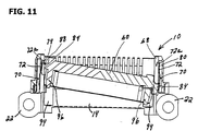
- Figure 11 shows shutter plate 60 in a skewed or cocked position within housing 14 of connector 10. This depiction may show the shutter plate in its most extreme cocked position, but it clearly shows how the flexible locating means provided by leaf springs 72 are effective to allow the shutter plate to move in directions longitudinally of connector housing 14 without the shutter plate binding relative to the housing. In essence, the flexibility of the leaf springs allow the shutter plate to yield relative to the housing to prevent binding of the shutter plate upon movement relative to the housing between the protective and retracted positions of the shutter plate.
Landscapes
- Connector Housings Or Holding Contact Members (AREA)
- Details Of Connecting Devices For Male And Female Coupling (AREA)
- Coupling Device And Connection With Printed Circuit (AREA)
Applications Claiming Priority (2)
| Application Number | Priority Date | Filing Date | Title |
|---|---|---|---|
| JP2001360197 | 2001-11-27 | ||
| JP2001360197A JP3981942B2 (ja) | 2001-11-27 | 2001-11-27 | 電気コネクタ |
Publications (2)
| Publication Number | Publication Date |
|---|---|
| EP1315247A2 true EP1315247A2 (de) | 2003-05-28 |
| EP1315247A3 EP1315247A3 (de) | 2005-04-27 |
Family
ID=19171057
Family Applications (1)
| Application Number | Title | Priority Date | Filing Date |
|---|---|---|---|
| EP02026234A Withdrawn EP1315247A3 (de) | 2001-11-27 | 2002-11-26 | Elektrischer Steckverbinder mit Abdeck- und Ausrichtmitteln |
Country Status (4)
| Country | Link |
|---|---|
| US (1) | US6767227B2 (de) |
| EP (1) | EP1315247A3 (de) |
| JP (1) | JP3981942B2 (de) |
| CN (1) | CN1302581C (de) |
Families Citing this family (9)
| Publication number | Priority date | Publication date | Assignee | Title |
|---|---|---|---|---|
| JP4145236B2 (ja) | 2003-11-21 | 2008-09-03 | ヒロセ電機株式会社 | 電気コネクタ装置 |
| TWM269611U (en) * | 2004-12-23 | 2005-07-01 | Cheng Uei Prec Ind Co Ltd | Dustproof receptacle connector |
| US7229327B2 (en) | 2005-05-25 | 2007-06-12 | Alcoa Fujikura Limited | Canted coil spring power terminal and sequence connection system |
| US7294020B2 (en) * | 2005-05-25 | 2007-11-13 | Alcoa Fujikura Ltd. | Canted coil spring power terminal and sequence connection system |
| JP2009176607A (ja) * | 2008-01-25 | 2009-08-06 | Fujitsu Ltd | 部品支持装置 |
| JP5080692B2 (ja) * | 2009-09-01 | 2012-11-21 | オリンパスメディカルシステムズ株式会社 | 電気コネクタ及び内視鏡 |
| US8988860B2 (en) * | 2012-11-29 | 2015-03-24 | Siemens Aktiengesellschaft | Power supplies having power electronic modules and replacement methods thereof |
| JP6162546B2 (ja) * | 2013-08-30 | 2017-07-12 | 矢崎総業株式会社 | コネクタ |
| CN104682092B (zh) * | 2013-12-03 | 2017-05-10 | 河北建筑工程学院 | 一种弱磁力定位接插件 |
Citations (1)
| Publication number | Priority date | Publication date | Assignee | Title |
|---|---|---|---|---|
| US5281156A (en) * | 1993-02-18 | 1994-01-25 | Yi Lee M | Safety electrical receptacle |
Family Cites Families (24)
| Publication number | Priority date | Publication date | Assignee | Title |
|---|---|---|---|---|
| US3795888A (en) * | 1972-06-30 | 1974-03-05 | Motorola Inc | Printed circuit board edge connector requiring zero insertion force |
| US3920303A (en) * | 1973-08-20 | 1975-11-18 | Ind Electronic Hardware Corp | Low force insertion connector |
| US4650268A (en) * | 1984-03-02 | 1987-03-17 | Dart Industries Inc. | Cordless iron |
| JPH059827Y2 (de) * | 1986-05-02 | 1993-03-10 | ||
| DE3789466T2 (de) * | 1986-03-17 | 1994-07-28 | Fujisawa Pharmaceutical Co | 3,7-Disubstituierte-3-Cephemverbindungen und Verfahren zu ihrer Herstellung. |
| JPS63242692A (ja) * | 1987-03-31 | 1988-10-07 | 三菱電機株式会社 | 半導体装置カ−ド |
| JP2534204B2 (ja) | 1987-03-31 | 1996-09-11 | 三菱電機株式会社 | 半導体装置カ−ド |
| US4867693A (en) * | 1988-08-01 | 1989-09-19 | General Electric Company | Safety electrical tap |
| JPH0650270A (ja) | 1991-04-15 | 1994-02-22 | Shuichi Kitamura | 非接触回転機械の羽根と回転中心体とを有するローターの構築方法 |
| US5167516A (en) * | 1991-08-21 | 1992-12-01 | Foxconn International, Inc. | Connection with floating shield |
| DE4238202C2 (de) * | 1991-11-11 | 1994-10-20 | Kansei Kk | Elektrischer Steckverbinder |
| CN2161000Y (zh) * | 1993-04-17 | 1994-04-06 | 肖桂华 | 自动关闭防尘防触电安全插座 |
| JP2587452Y2 (ja) * | 1993-12-14 | 1998-12-16 | ヒロセ電機株式会社 | 低挿抜力電気コネクタ |
| US6016306A (en) * | 1993-12-24 | 2000-01-18 | International Business Machines Corporation | Routing bandwidth-reserved connections in information networks |
| JP2825445B2 (ja) * | 1994-08-31 | 1998-11-18 | 矢崎総業株式会社 | コネクタ |
| CN1155773A (zh) * | 1995-11-17 | 1997-07-30 | 住友电装株式会社 | 可检测不完全接合的连接件 |
| JP3173438B2 (ja) * | 1997-06-04 | 2001-06-04 | ソニー株式会社 | メモリカード及び装着装置 |
| US5944542A (en) * | 1997-06-27 | 1999-08-31 | Han Y. Lee | Plug safety adapter for anti-electric shock |
| US6015306A (en) | 1997-09-30 | 2000-01-18 | Jen; Tsang Lan | Shutter structure of aperture |
| US6102715A (en) * | 1998-02-10 | 2000-08-15 | The Great American Gumball Corporation | Personal computer peripheral device adapter |
| JP3285321B2 (ja) * | 1998-02-26 | 2002-05-27 | 日本圧着端子製造株式会社 | カード接続用アダプタ |
| FR2785728B1 (fr) * | 1998-07-24 | 2004-03-26 | Whitaker Corp | Assemblage de connecteurs electriques |
| US6109940A (en) * | 1998-10-09 | 2000-08-29 | Methode Electronics, Inc. | Shutter mechanism for card adapter |
| US6179479B1 (en) * | 1999-07-09 | 2001-01-30 | Veam S.R.L. | Fiber optic connector with self-closing shutter |
-
2001
- 2001-11-27 JP JP2001360197A patent/JP3981942B2/ja not_active Expired - Fee Related
-
2002
- 2002-11-22 US US10/303,093 patent/US6767227B2/en not_active Expired - Fee Related
- 2002-11-26 CN CNB021518203A patent/CN1302581C/zh not_active Expired - Fee Related
- 2002-11-26 EP EP02026234A patent/EP1315247A3/de not_active Withdrawn
Patent Citations (1)
| Publication number | Priority date | Publication date | Assignee | Title |
|---|---|---|---|---|
| US5281156A (en) * | 1993-02-18 | 1994-01-25 | Yi Lee M | Safety electrical receptacle |
Also Published As
| Publication number | Publication date |
|---|---|
| CN1438737A (zh) | 2003-08-27 |
| JP3981942B2 (ja) | 2007-09-26 |
| US6767227B2 (en) | 2004-07-27 |
| US20030124889A1 (en) | 2003-07-03 |
| CN1302581C (zh) | 2007-02-28 |
| JP2003168527A (ja) | 2003-06-13 |
| EP1315247A3 (de) | 2005-04-27 |
Similar Documents
| Publication | Publication Date | Title |
|---|---|---|
| US6860750B1 (en) | Cable end connector assembly having locking member | |
| US6379187B2 (en) | Electrical connector | |
| US7806739B2 (en) | Battery connector with time-delay function | |
| US7179126B2 (en) | Electrical connector with improved terminals | |
| US6716069B2 (en) | Connector with a housing and a retainer held securely on the housing | |
| US20050227524A1 (en) | Modular jack with a detective switch | |
| US7534140B2 (en) | Electrical connector with improved metal spring | |
| US6431907B1 (en) | FPC connector with positioning actuator | |
| EP0746062B1 (de) | Flächenverbindbarer elektrischer Steckverbinder | |
| US7789699B2 (en) | Flexible printed circuit connector and slider | |
| US7670174B2 (en) | Low profile electrical connector | |
| US6942503B2 (en) | Electrical connector with grounded shutter member | |
| US6767227B2 (en) | Electrical connector | |
| US6077092A (en) | Electrical connector having stabilizing structure for spacer and terminal | |
| US6918794B2 (en) | Modular jack having an anti-mismating member to prevent incorrect insertion of a smaller sized plug | |
| US20040166739A1 (en) | Electrical connector with a terminal pin stabilizing plate | |
| US4350402A (en) | Board mount zero insertion force connector | |
| US6986671B2 (en) | Board mounted electrical connector assembly | |
| US6302748B1 (en) | Electrical connector having an improved housing with reliable contact receiving cavities | |
| US7118396B2 (en) | Electrical card connector | |
| US7029319B2 (en) | Flat circuit connector | |
| EP0997987A2 (de) | Schwimmend gelagerter Verbinder zum Verbinden elektrischer Baugruppen | |
| US20050070173A1 (en) | Pogo type antenna connector | |
| US20070167076A1 (en) | Electrical connector having protective shutter | |
| US6666714B1 (en) | Electrical connector with terminal protector |
Legal Events
| Date | Code | Title | Description |
|---|---|---|---|
| PUAI | Public reference made under article 153(3) epc to a published international application that has entered the european phase |
Free format text: ORIGINAL CODE: 0009012 |
|
| AK | Designated contracting states |
Designated state(s): AT BE BG CH CY CZ DE DK EE ES FI FR GB GR IE IT LI LU MC NL PT SE SK TR |
|
| AX | Request for extension of the european patent |
Extension state: AL LT LV MK RO SI |
|
| PUAL | Search report despatched |
Free format text: ORIGINAL CODE: 0009013 |
|
| AK | Designated contracting states |
Kind code of ref document: A3 Designated state(s): AT BE BG CH CY CZ DE DK EE ES FI FR GB GR IE IT LI LU MC NL PT SE SK TR |
|
| AX | Request for extension of the european patent |
Extension state: AL LT LV MK RO SI |
|
| 17P | Request for examination filed |
Effective date: 20051020 |
|
| AKX | Designation fees paid |
Designated state(s): DE FR GB IT |
|
| 17Q | First examination report despatched |
Effective date: 20060111 |
|
| STAA | Information on the status of an ep patent application or granted ep patent |
Free format text: STATUS: THE APPLICATION IS DEEMED TO BE WITHDRAWN |
|
| 18D | Application deemed to be withdrawn |
Effective date: 20070220 |