EP1319260B1 - Commutateur de guide d'ondes coplanaire - Google Patents
Commutateur de guide d'ondes coplanaire Download PDFInfo
- Publication number
- EP1319260B1 EP1319260B1 EP01955268A EP01955268A EP1319260B1 EP 1319260 B1 EP1319260 B1 EP 1319260B1 EP 01955268 A EP01955268 A EP 01955268A EP 01955268 A EP01955268 A EP 01955268A EP 1319260 B1 EP1319260 B1 EP 1319260B1
- Authority
- EP
- European Patent Office
- Prior art keywords
- connection
- capacitor
- capacitance
- signal line
- waveguide
- Prior art date
- Legal status (The legal status is an assumption and is not a legal conclusion. Google has not performed a legal analysis and makes no representation as to the accuracy of the status listed.)
- Expired - Lifetime
Links
- 239000003990 capacitor Substances 0.000 claims description 36
- 239000000758 substrate Substances 0.000 description 18
- 239000002184 metal Substances 0.000 description 10
- 229910052751 metal Inorganic materials 0.000 description 10
- 230000008901 benefit Effects 0.000 description 4
- 238000003780 insertion Methods 0.000 description 4
- 230000037431 insertion Effects 0.000 description 4
- 150000001875 compounds Chemical class 0.000 description 3
- 238000010586 diagram Methods 0.000 description 3
- VYPSYNLAJGMNEJ-UHFFFAOYSA-N Silicium dioxide Chemical compound O=[Si]=O VYPSYNLAJGMNEJ-UHFFFAOYSA-N 0.000 description 2
- 230000003044 adaptive effect Effects 0.000 description 2
- 238000002955 isolation Methods 0.000 description 2
- 239000000463 material Substances 0.000 description 2
- 238000000034 method Methods 0.000 description 2
- 238000007493 shaping process Methods 0.000 description 2
- 229910052581 Si3N4 Inorganic materials 0.000 description 1
- 230000006978 adaptation Effects 0.000 description 1
- 230000005540 biological transmission Effects 0.000 description 1
- 230000015572 biosynthetic process Effects 0.000 description 1
- 230000008859 change Effects 0.000 description 1
- 238000009413 insulation Methods 0.000 description 1
- 238000004519 manufacturing process Methods 0.000 description 1
- 239000012528 membrane Substances 0.000 description 1
- 150000002739 metals Chemical class 0.000 description 1
- 235000012239 silicon dioxide Nutrition 0.000 description 1
- 239000000377 silicon dioxide Substances 0.000 description 1
- HQVNEWCFYHHQES-UHFFFAOYSA-N silicon nitride Chemical compound N12[Si]34N5[Si]62N3[Si]51N64 HQVNEWCFYHHQES-UHFFFAOYSA-N 0.000 description 1
- 230000009466 transformation Effects 0.000 description 1
- 230000007704 transition Effects 0.000 description 1
Images

Classifications
-
- H—ELECTRICITY
- H01—ELECTRIC ELEMENTS
- H01P—WAVEGUIDES; RESONATORS, LINES, OR OTHER DEVICES OF THE WAVEGUIDE TYPE
- H01P1/00—Auxiliary devices
- H01P1/10—Auxiliary devices for switching or interrupting
-
- H—ELECTRICITY
- H01—ELECTRIC ELEMENTS
- H01P—WAVEGUIDES; RESONATORS, LINES, OR OTHER DEVICES OF THE WAVEGUIDE TYPE
- H01P1/00—Auxiliary devices
- H01P1/10—Auxiliary devices for switching or interrupting
- H01P1/12—Auxiliary devices for switching or interrupting by mechanical chopper
- H01P1/127—Strip line switches
-
- H—ELECTRICITY
- H01—ELECTRIC ELEMENTS
- H01H—ELECTRIC SWITCHES; RELAYS; SELECTORS; EMERGENCY PROTECTIVE DEVICES
- H01H59/00—Electrostatic relays; Electro-adhesion relays
- H01H59/0009—Electrostatic relays; Electro-adhesion relays making use of micromechanics
Definitions
- Micromechanically fabricated high-frequency shorting switches consist of a thin metal bridge, which is stretched between the ground lines of a coplanar waveguide. Electrostatically, this bridge is pulled onto a thin dielectric, which is applied to the signal line, whereby the capacitance of the plate capacitor formed from bridge and signal line is increased. This capacitance between the signal line and ground line affects the propagation characteristics of the electromagnetic waves carried on the waveguide. In the “Off” booth (the metal bridge is below) much of the power is reflected. In the “on” state (the metal bridge is on top), much of the power is transmitted.
- a micromechanical switch is known, for example, from the document " Barker et al .: Distributed MEMS True-Time Delay 'Phase Shifters and Wide Band Switches', IEEE Transactions on Microwave Theory and Techniques, Vol. 46, No. 11, 1998, pages 1881-1889 , known. It is var forward to provide a plurality of parallel microbridges, each having a certain width and a certain distance from each other.
- microswitches are here by so-called cantilever, so clamped on one side. Microbar, trained.
- the device according to the invention with the features of the main claim has the advantage that the second connection is mechanically deformable so that the distance of the first connection and the second connection can be changed at least in a partial region of the second connection.
- a capacitor is produced by simple means whose capacity is variable.
- the length of the metal bridge ie the length of the second electrically conductive connection
- the distance of the ground lines of the coplanar waveguide can be chosen independently of the length of the second connection and vice versa.
- the first and second compounds are metallic compounds.
- all material-specific and process-technical advantages of the use of metals as electrically conductive compounds are used according to the invention.
- the capacitance change of the capacitor can be effected by an electrostatic force between the first connection and the second connection.
- the capacitor has a first predetermined capacitance and a second predetermined capacitance as a function of a predetermined electrical voltage between the first connection and the second connection.
- This makes it possible, by dimensioning in particular the first and second electrically conductive connection and the dielectric layer between the two, to determine the operating frequency within wide limits, independently of the distance of the ground lines of the coplanar waveguide.
- the insertion loss is adjustable thereby.
- the first connection forms an inductance in series with the capacitor between the signal line and the ground lines. This makes it possible to provide different shapes and dimensions for the first connection, so that the inductance resulting from the first connection can be predetermined within wide limits.
- the common impedance of the first capacitance and the inductance at an operating frequency substantially corresponds to its ohmic resistance. This makes it possible to achieve a particularly large insulation, ie a particularly large reflection coefficient, with switched off short circuit.
- the predetermined length is advantageously provided in such a way that reflections compensate at a transition between the signal line and the second connection. As a result, the insertion loss of the switch and thus the adjustment in the on state is improved.
- FIG. 1 shows a micromechanical high-frequency short circuit switch as an example of the device according to the invention with a capacitor.
- a coplanar waveguide is applied to a substrate 100.
- the coplanar waveguide consists in particular of three coplanar electrically conductive lines which, at least locally, are guided substantially parallel to one another.
- the lines of the coplanar waveguide are provided in particular metallic and applied to the substrate in particular by means of one or more galvanic process steps.
- the substrate 100 according to the invention has in particular the property of having a low loss angle.
- the two outer ones of the three lines of the coplanar waveguide correspond to a first ground line 110 and a second ground line 111, and the middle line corresponds to a signal line 120 of the coplanar waveguide.
- FIG. 1 is shown in plan view of interest for the inventive device section of such guided on the substrate 100 coplanar waveguide.
- the two ground lines 110, 111 of the coplanar waveguide are connected by means of a first electrically conductive connection 130.
- the first connection 130 is applied directly to the substrate 100 and has a small "height" in comparison to the "height" of the ground lines 110, 111, ie, the first connection 130 connects the ground lines 110, 111 to their "foot" the substrate 100.
- the signal line 120 of the coplanar waveguide is interrupted. Therefore, the connection 130 is also not electrically connected to the signal line 120.
- a layer of an in FIG. 1 Not applied dielectric applied.
- the interrupted signal line 120 is connected by means of a second electrically conductive connection 121.
- the second connection 121 is hereby provided according to the invention, in particular in the form of a metal connecting bridge between the ends of the interrupted signal line 120.
- the second connection 121 is provided at a certain distance from the plane of the substrate 100, wherein the distance between the second connection 121 to the substrate 100 and to the first connection 130 corresponds approximately to the height of the signal line 120.
- the second connection 121 In this respect, the second connection 121 "floats" between the ends of the interrupted signal line 120.
- the second connection 121 is also referred to as a bridge or metal bridge 121.
- a first, designated by the letter C cutting line, a designated by the letter A second cutting line and a letter marked with the third B section line are shown.
- the first cut line intersects the device according to the invention perpendicular to the course of the ground lines 110, 111 and the signal line 120 in the region of the first connection 130 between the ground lines 110, 111.
- the second section line intersects the device according to the invention parallel to the course of the lines 110, 111, 120 of coplanar waveguide in the region of the first ground line 110.
- the third section line cuts the device according to the invention parallel to the path of the lines 110, 111, 120 of the coplanar waveguide in the region of the signal line 120 or - where the signal line 120 is interrupted - in the region of the second connection 121st
- FIG. 2 is a sectional view of the device according to the invention along the first section line (letter C) from the FIG. 1 shown. It is the substrate again 100, the first ground line 110 and the second ground line 111 of the coplanar waveguide are shown. Between the ground lines 110, 111 of the coplanar waveguide, the signal line 120 of the waveguide is arranged.
- the spatial arrangement of the first connection 130 and the second connection 121 with respect to their distance from the surface of the substrate 100 is particularly clear.
- the first connection 130 is in FIG. 2 applied directly to the substrate 100, while the second connection 121 is applied to the signal line 120 and thus provided at a distance from the height of the signal or ground line 110, 111, 120 away from the plane of the substrate 100.
- FIG. 3 is the device according to the invention in a sectional view along the section line A from FIG. 1 shown. Only the substrate 100 and the first ground line 110 are visible.
- FIG. 4 the device according to the invention along the third section line (letter B) is shown.
- the signal line 120 of the coplanar waveguide is provided on the substrate 100.
- the signal line 120 is interrupted at a predetermined length 122.
- the second connection 121 bridges the signal line 120.
- the second connection 121 connects the two ends of the signal line 120 caused by the interruption of the signal line 120.
- the second connection 121 is provided in the exemplary embodiment, in particular at a distance from the substrate 100 the height of the signal line 120 corresponds.
- the first connection 130 is shown. Above the first connection 130 is already in connection with FIG. 1 addressed dielectric layer 140.
- FIG. 5 the device according to the invention is shown in perspective view.
- the substrate 100 On the substrate 100 is the first ground line 110 and the second ground line 111 of the waveguide. Between these ground lines 110, 111 is the interrupted signal line 120. The two ends of the signal line 120 are bridged by the second connection 121.
- the dielectric layer 140 is shown.
- the first connection 130 between the ground lines 110, 111 provided below the dielectric layer 140, ie in the direction of the substrate 100, is shown in FIG FIG. 5 not shown.
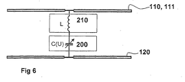
- FIG. 6 an equivalent circuit diagram of the arrangement according to the invention is shown.
- the two ground lines 110, 111 are shown only in the form of a single line of the coplanar waveguide. This is because the ground lines 110, 111 are at the same potential.
- the signal line 120 of the coplanar waveguide is in FIG. 6 shown.
- a capacitor 200 and an inductance 210 are arranged in series. The capacitor 200 is at least partially connected through the first connection 130 and the second connection 121, both in FIG FIG. 6 not shown realized.
- the capacitor 200 is provided variable in its capacity, and indeed according to the invention in particular the fact that the second connection 121 mechanically deformed and thus at least in some areas their distance to the first connection 130 changes, which affects the capacitance of the capacitor 200.
- the inductance 210 is essentially realized by the first connection 130.
- an inductance is generated, which can be predetermined by changing the length-width ratio, the shape, for example meandering or the like.
- the mechanically deformable second connection 121 is illustrated in the case in which the illustrated section of the coplanar waveguide has a high transmission coefficient and a low reflection coefficient.
- the distance between the first connection 130 and the second connection 121, which together with the electrical properties of the dielectric layer 140 decisively determine the capacitance of the capacitor 200, are in FIG FIG. 4 shown at maximum distance.
- the capacitance of the capacitor 200 is very small in this case and is decisive for the input attenuation of, for example, a short-circuit switch.
- an electrical voltage for example a DC voltage
- the second connection 121 since it is mechanically deformable, deformed and pulled into at least one subarea, namely essentially in the middle of the metal bridge, to the first connection 130 or to the dielectric layer 140 applied to the first connection 130.
- the dielectric in particular silicon dioxide or silicon nitride, prevents a galvanic contact of the device designed in particular as a switch in the off state.
- the capacitance of the capacitor 200 that is significantly formed from the first connection 130 and the second connection 121 changes, so that its capacitance becomes greater.
- the application or removal of an electrical voltage between the two connections 130, 121, the capacitance of the capacitor 200 of the device according to the invention changed and switched in the formation of the device as a switch.
- FIGS. 4 and 5 illustrated position of the second connection 121 corresponds to the operation of the device with passage and is switched as a switched-state.
- the in FIG. 4 not shown state of an attracted by an electrical voltage to the first connection 130 second connection 121 corresponds to an off switch. This is the case because it is provided according to the invention that the waveguide, which in the FIGS. 1 to 4 illustrated section is operated at a predetermined operating frequency.
- the capacitance of the capacitor 200 depending on an electrical voltage between the two connections 130, 121, assumes two capacitance values, which are referred to below as the first capacitance value or first capacitance and as the second capacitance value or second capacitance.
- the first capacitor corresponds to the switched-off state, ie, the first connection 121 is attracted to the first connection 130 due to the applied electrical voltage.
- the second capacity thus corresponds to the in FIG. 4 shown switched case where the second connection 121 is not mechanically deformed.
- the first capacitance and the second capacitance are determined by varying in particular the width and length of the first connection 130 and the second connection 121 as well as the thickness and the material properties of the dielectric layer and the height of the signal line 120.
- connections 130, 121, the dielectric layer 140 and the signal line 120 are dimensioned so that the impedance of a series connection of the first capacitor and an inductance formed by the first connection 130 in the Operating frequency is just canceled, or is as small as possible.
- the adjustment of the inductance 210 is done according to the invention essentially by the dimensioning and shaping of the first connection 130 between the ground lines 110, 111 of the waveguide.
- the second connection 121 is a thin metal bridge, which is stretched between the ends of the interrupted signal line 120 of the waveguide. Between the ground lines 110, 111, the first connection 130 acts as a DC short circuit.
- the first connection 130 acts with the second connection 121 as a plate capacitor.
- an inductance arranged in series with the plate capacitor can be set.
- a series resonant circuit is formed whose resonant frequency is in the off state of the second connection 121 by appropriate dimensioning of inductance and capacitance of the plate capacitor at the operating frequency of the device.
- the impedance between signal line 120 and the ground lines 110, 111 is greatly reduced compared to the impedance of the pure plate capacitor (without inductance), which significantly improves the isolation of a device designed as a high-frequency switch.
- the isolation is now limited by the ohmic losses in the second connection 121 and in the first connection 130.
- the device or the component or component at operating frequency by the reduced capacitance of the plate capacitor (second connection 121 or Bridge 121 " Up ", ie with a relatively large distance from the substrate) operated outside of this resonant frequency, so that no higher insertion loss results.
- the length of the second connection 121 is suitably dimensioned (eg half of the effective wavelength at the operating frequency)
- the reflections at the junctions or junctions between the coplanar waveguide (ie the ends of the signal line 120) and the second connection 121 compensate each other , whereby the insertion loss of the example provided as a switch Vorsch and thus the adaptation can be improved.
- the length of the second connection 121 is not limited by a maximum distance of the ground lines at high operating frequencies. As a result, at higher operating frequencies no increased switching voltage, ie between the first and the second connection 130 121 to be applied voltage to spend.
- the device according to the invention is particularly suitable for applications in the field of ACC (Adaptive Cruise Control) or SRR (Short Range Radar).
- ACC Adaptive Cruise Control
- SRR Short Range Radar
Landscapes
- Waveguide Switches, Polarizers, And Phase Shifters (AREA)
- Waveguides (AREA)
Claims (8)
- Dispositif comportant un condensateur (200) pour modifier l'impédance d'une pièce d'un guide d'onde coplanaire,
selon lequel:la capacité du condensateur (200) peut être modifiée,le condensateur (200) comporte au moins en partie une première liaison électroconductrice (130) et une seconde liaison électroconductrice (121), la ligne de signal (120) de la pièce du guide d'onde étant interrompue sur une longueur prédéfinie (122),la première liaison (130) reliant les lignes de masse (110, 111) du guide d'onde, etla seconde liaison (121) reliant les deux parties de la ligne de signal (120), interrompue,caractérisé en ce que
pour modifier la capacité, la seconde liaison (121) est réalisée sous la forme d'un pont de liaison sur la première liaison (130) en étant déformable mécaniquement pour modifier la distance de la première liaison (130) et de la seconde liaison (121) au moins dans une zone partielle de la seconde liaison (121). - Dispositif selon la revendication 1,
caractérisé en ce que
la première et la seconde liaison (130, 121) sont des liaisons métalliques. - Dispositif selon l'une des revendications précédentes,
caractérisé en ce que
la variation de capacité du condensateur (200) est assurée par une force électrostatique entre la première liaison (130) et la seconde liaison (121). - Dispositif selon l'une des revendications précédentes,
caractérisé en ce que
le condensateur (120) présente une première capacité prédéfinie et une seconde capacité prédéfinie en fonction d'une tension électrique prédéterminée entre la première liaison (130) et la seconde liaison (121). - Dispositif selon l'une des revendications précédentes,
caractérisé en ce que
la première liaison (130) forme une inductance (120) en série avec le condensateur (200) entre la ligne de signal (120) et les lignes de masse (1110, 111). - Dispositif selon la revendication 5,
caractérisé en ce que
l'impédance commune de la première capacité et de l'inductance (210) correspond pratiquement à sa résistance ohmique.par la fréquence de fonctionnement. - Dispositif selon la revendication 6,
caractérisé en ce que
la fréquence de fonctionnement est de l'ordre de 77 GHz ou de l'ordre de 24 GHz. - Dispositif selon l'une des revendications précédentes,
caractérisé en ce que
la longueur prédéfinie (122) est prévue de façon que les réflexions à la jonction entre la ligne de signal (120) et la première liaison (121) se compensent.
Applications Claiming Priority (3)
| Application Number | Priority Date | Filing Date | Title |
|---|---|---|---|
| DE10037385 | 2000-08-01 | ||
| DE10037385A DE10037385A1 (de) | 2000-08-01 | 2000-08-01 | Vorrichtung mit einem Kondensator |
| PCT/DE2001/002757 WO2002011232A1 (fr) | 2000-08-01 | 2001-07-20 | Commutateur de guide d'ondes coplanaire |
Publications (2)
| Publication Number | Publication Date |
|---|---|
| EP1319260A1 EP1319260A1 (fr) | 2003-06-18 |
| EP1319260B1 true EP1319260B1 (fr) | 2008-08-20 |
Family
ID=7650904
Family Applications (1)
| Application Number | Title | Priority Date | Filing Date |
|---|---|---|---|
| EP01955268A Expired - Lifetime EP1319260B1 (fr) | 2000-08-01 | 2001-07-20 | Commutateur de guide d'ondes coplanaire |
Country Status (6)
| Country | Link |
|---|---|
| US (1) | US6686810B2 (fr) |
| EP (1) | EP1319260B1 (fr) |
| JP (1) | JP2004505578A (fr) |
| KR (1) | KR20020035624A (fr) |
| DE (2) | DE10037385A1 (fr) |
| WO (1) | WO2002011232A1 (fr) |
Families Citing this family (11)
| Publication number | Priority date | Publication date | Assignee | Title |
|---|---|---|---|---|
| DE10051311C1 (de) | 2000-10-17 | 2002-03-14 | Bosch Gmbh Robert | Vorrichtung mit einer Kondensatoranordnung |
| DE10100296A1 (de) | 2001-01-04 | 2002-07-11 | Bosch Gmbh Robert | Vorrichtung mit einem Kondensator mit veränderbarer Kapazität, insbesondere Hochfrequenz-Mikroschalter |
| DE10229038B4 (de) * | 2002-06-28 | 2013-08-14 | Robert Bosch Gmbh | Verkapptes Mikrostrukturbauelement mit Hochfrequenzdurchführung |
| US20060097388A1 (en) | 2002-07-02 | 2006-05-11 | Klaus Breitschwerdt | Electrical system, especially a microelectronic or microelectromechanical high frequency system |
| DE10342938A1 (de) * | 2003-09-17 | 2005-04-21 | Bosch Gmbh Robert | Bauteil zu Impedanzänderung bei einem koplanaren Wellenleiter sowie Verfahren zu Herstellung eines Bauelements |
| DE102006001321B3 (de) * | 2006-01-09 | 2007-07-26 | Protron Mikrotechnik Gmbh | Mikromechanischer Hochfrequenz-Schalter für koplanare Wellenleiter |
| DE102007035633B4 (de) | 2007-07-28 | 2012-10-04 | Protron Mikrotechnik Gmbh | Verfahren zur Herstellung mikromechanischer Strukturen sowie mikromechanische Struktur |
| CN103474734B (zh) * | 2013-08-20 | 2016-08-10 | 京信通信技术(广州)有限公司 | 电桥 |
| CA2852858A1 (fr) * | 2014-05-30 | 2015-11-30 | C-Com Satellite Systems Inc. | Dispositif de decalage de phase |
| US11515609B2 (en) * | 2019-03-14 | 2022-11-29 | Taiwan Semiconductor Manufacturing Company, Ltd. | Transmission line structures for millimeter wave signals |
| DE102019126433A1 (de) | 2019-03-14 | 2020-09-17 | Taiwan Semiconductor Manufacturing Company, Ltd. | Übertragungsleitungsstrukturen für Millimeterwellensignale |
Citations (1)
| Publication number | Priority date | Publication date | Assignee | Title |
|---|---|---|---|---|
| US5619061A (en) * | 1993-07-27 | 1997-04-08 | Texas Instruments Incorporated | Micromechanical microwave switching |
Family Cites Families (4)
| Publication number | Priority date | Publication date | Assignee | Title |
|---|---|---|---|---|
| US5087896A (en) * | 1991-01-16 | 1992-02-11 | Hughes Aircraft Company | Flip-chip MMIC oscillator assembly with off-chip coplanar waveguide resonant inductor |
| US5528203A (en) * | 1994-09-26 | 1996-06-18 | Endgate Corporation | Coplanar waveguide-mounted flip chip |
| CA2211830C (fr) | 1997-08-22 | 2002-08-13 | Cindy Xing Qiu | Commutateurs hyperfrequence electromagnetiques miniatures et plaquettes de commutateurs |
| KR100344790B1 (ko) * | 1999-10-07 | 2002-07-19 | 엘지전자주식회사 | 마이크로 기계구조를 이용한 주파수 가변 초고주파 필터 |
-
2000
- 2000-08-01 DE DE10037385A patent/DE10037385A1/de not_active Withdrawn
-
2001
- 2001-07-20 EP EP01955268A patent/EP1319260B1/fr not_active Expired - Lifetime
- 2001-07-20 JP JP2002516855A patent/JP2004505578A/ja active Pending
- 2001-07-20 DE DE50114251T patent/DE50114251D1/de not_active Expired - Lifetime
- 2001-07-20 US US10/089,618 patent/US6686810B2/en not_active Expired - Fee Related
- 2001-07-20 WO PCT/DE2001/002757 patent/WO2002011232A1/fr not_active Ceased
- 2001-07-20 KR KR1020027004157A patent/KR20020035624A/ko not_active Withdrawn
Patent Citations (1)
| Publication number | Priority date | Publication date | Assignee | Title |
|---|---|---|---|---|
| US5619061A (en) * | 1993-07-27 | 1997-04-08 | Texas Instruments Incorporated | Micromechanical microwave switching |
Also Published As
| Publication number | Publication date |
|---|---|
| DE50114251D1 (de) | 2008-10-02 |
| DE10037385A1 (de) | 2002-02-14 |
| US20030030505A1 (en) | 2003-02-13 |
| US6686810B2 (en) | 2004-02-03 |
| EP1319260A1 (fr) | 2003-06-18 |
| KR20020035624A (ko) | 2002-05-11 |
| WO2002011232A1 (fr) | 2002-02-07 |
| JP2004505578A (ja) | 2004-02-19 |
Similar Documents
| Publication | Publication Date | Title |
|---|---|---|
| DE60308100T2 (de) | Hochfrequenzschalter und diesen verwendende elektronische Vorrichtung | |
| DE60314875T2 (de) | Mikroelektromechanischer hf-schalter | |
| DE60312665T2 (de) | Haltlos elektrostatisch aktiviertes mikroelektromechanisches Schaltsystem | |
| DE69609458T2 (de) | Elektromechanischer RF-Micro-Schalter | |
| DE69228146T2 (de) | Verbesserte Miniatur-Abstimmschaltung für Mikrowellen und Millimeterwellen | |
| EP1319260B1 (fr) | Commutateur de guide d'ondes coplanaire | |
| DE60007736T2 (de) | Mikromechanischer schalter und entsprechendes herstellungsverfahren | |
| DE60305349T2 (de) | Übergang von einem rechteckigen hohlleiter auf eine mikrostreifenleitung | |
| EP1266422A1 (fr) | Dephaseur et dispositif comprenant plusieurs dephaseurs | |
| DE60223479T2 (de) | Angepasste Breitband-Schaltmatrix mit aktiver Diode Isolation | |
| DE60307136T2 (de) | Mikromechanischer elektrostatischer schalter mit niedriger betätigungsspannung | |
| DE69930169T2 (de) | Mikromechanischer schalter | |
| EP1350281B1 (fr) | Dispositif dote d'un condensateur a capacite variable, en particulier commutateur miniature a haute frequence | |
| DE10051311C1 (de) | Vorrichtung mit einer Kondensatoranordnung | |
| DE69837078T2 (de) | Verlustarmer luftgelagerter radial kombinierter Streifenleiter für N-Weg-RF-Schalter | |
| EP1665315B1 (fr) | Composant pour la modification de l'impedance dans un guide d'ondes coplanaire, et procede de production d'un tel composant | |
| EP4092914B1 (fr) | Antennes couplées au rayonnement en réseau | |
| DE60307672T2 (de) | Mikromechanischer elektrostatischer schalter mit niedriger betätigungsspannung | |
| DE60314470T2 (de) | Netzwerk zur Vorspannungsversorgung für symmetrische Leitungen | |
| EP1719144B1 (fr) | Interrupteur mems haute frequence comportant un element de commutation courbe, et son procede de production | |
| EP1702386A1 (fr) | Coupleur directionnel a espace de couplage important | |
| Muldavin et al. | Novel series and shunt MEMS switch geometries for X-band applications | |
| EP1495513A1 (fr) | Reseau d'adaptation electrique pourvu d'une ligne de transformation | |
| DE102004062992A1 (de) | Schaltbares Hochfrequenz-MEMS-Element mit bewegbarem Schaltelement und Verfahren zu einer Herstellung | |
| DE10238947A1 (de) | Koplanarer Phasenschieber mit konstanter Dämpfung |
Legal Events
| Date | Code | Title | Description |
|---|---|---|---|
| PUAI | Public reference made under article 153(3) epc to a published international application that has entered the european phase |
Free format text: ORIGINAL CODE: 0009012 |
|
| 17P | Request for examination filed |
Effective date: 20030303 |
|
| AK | Designated contracting states |
Designated state(s): AT BE CH CY DE DK ES FI FR GB GR IE IT LI LU MC NL PT SE TR |
|
| RBV | Designated contracting states (corrected) |
Designated state(s): AT BE CH DE FR GB IT LI |
|
| 17Q | First examination report despatched |
Effective date: 20070713 |
|
| GRAP | Despatch of communication of intention to grant a patent |
Free format text: ORIGINAL CODE: EPIDOSNIGR1 |
|
| RBV | Designated contracting states (corrected) |
Designated state(s): CH DE FR GB IT LI |
|
| GRAS | Grant fee paid |
Free format text: ORIGINAL CODE: EPIDOSNIGR3 |
|
| GRAA | (expected) grant |
Free format text: ORIGINAL CODE: 0009210 |
|
| AK | Designated contracting states |
Kind code of ref document: B1 Designated state(s): CH DE FR GB IT LI |
|
| REG | Reference to a national code |
Ref country code: GB Ref legal event code: FG4D Free format text: NOT ENGLISH |
|
| REG | Reference to a national code |
Ref country code: CH Ref legal event code: EP |
|
| REF | Corresponds to: |
Ref document number: 50114251 Country of ref document: DE Date of ref document: 20081002 Kind code of ref document: P |
|
| PLBE | No opposition filed within time limit |
Free format text: ORIGINAL CODE: 0009261 |
|
| STAA | Information on the status of an ep patent application or granted ep patent |
Free format text: STATUS: NO OPPOSITION FILED WITHIN TIME LIMIT |
|
| 26N | No opposition filed |
Effective date: 20090525 |
|
| PGFP | Annual fee paid to national office [announced via postgrant information from national office to epo] |
Ref country code: CH Payment date: 20100726 Year of fee payment: 10 |
|
| PGFP | Annual fee paid to national office [announced via postgrant information from national office to epo] |
Ref country code: GB Payment date: 20100726 Year of fee payment: 10 |
|
| REG | Reference to a national code |
Ref country code: CH Ref legal event code: PL |
|
| GBPC | Gb: european patent ceased through non-payment of renewal fee |
Effective date: 20110720 |
|
| PG25 | Lapsed in a contracting state [announced via postgrant information from national office to epo] |
Ref country code: CH Free format text: LAPSE BECAUSE OF NON-PAYMENT OF DUE FEES Effective date: 20110731 Ref country code: LI Free format text: LAPSE BECAUSE OF NON-PAYMENT OF DUE FEES Effective date: 20110731 |
|
| PG25 | Lapsed in a contracting state [announced via postgrant information from national office to epo] |
Ref country code: GB Free format text: LAPSE BECAUSE OF NON-PAYMENT OF DUE FEES Effective date: 20110720 |
|
| PGFP | Annual fee paid to national office [announced via postgrant information from national office to epo] |
Ref country code: FR Payment date: 20120803 Year of fee payment: 12 Ref country code: IT Payment date: 20120725 Year of fee payment: 12 |
|
| REG | Reference to a national code |
Ref country code: FR Ref legal event code: ST Effective date: 20140331 |
|
| PG25 | Lapsed in a contracting state [announced via postgrant information from national office to epo] |
Ref country code: IT Free format text: LAPSE BECAUSE OF NON-PAYMENT OF DUE FEES Effective date: 20130720 Ref country code: FR Free format text: LAPSE BECAUSE OF NON-PAYMENT OF DUE FEES Effective date: 20130731 |
|
| PGFP | Annual fee paid to national office [announced via postgrant information from national office to epo] |
Ref country code: DE Payment date: 20140925 Year of fee payment: 14 |
|
| REG | Reference to a national code |
Ref country code: DE Ref legal event code: R119 Ref document number: 50114251 Country of ref document: DE |
|
| PG25 | Lapsed in a contracting state [announced via postgrant information from national office to epo] |
Ref country code: DE Free format text: LAPSE BECAUSE OF NON-PAYMENT OF DUE FEES Effective date: 20160202 |