EP1320227A2 - Schaltvorrichtung mit Referenzkanal auf gemeinsame Spannung - Google Patents
Schaltvorrichtung mit Referenzkanal auf gemeinsame Spannung Download PDFInfo
- Publication number
- EP1320227A2 EP1320227A2 EP02080091A EP02080091A EP1320227A2 EP 1320227 A2 EP1320227 A2 EP 1320227A2 EP 02080091 A EP02080091 A EP 02080091A EP 02080091 A EP02080091 A EP 02080091A EP 1320227 A2 EP1320227 A2 EP 1320227A2
- Authority
- EP
- European Patent Office
- Prior art keywords
- interconnection
- points
- control
- matrix
- inputs
- Prior art date
- Legal status (The legal status is an assumption and is not a legal conclusion. Google has not performed a legal analysis and makes no representation as to the accuracy of the status listed.)
- Withdrawn
Links
Images



Classifications
-
- H—ELECTRICITY
- H04—ELECTRIC COMMUNICATION TECHNIQUE
- H04L—TRANSMISSION OF DIGITAL INFORMATION, e.g. TELEGRAPHIC COMMUNICATION
- H04L49/00—Packet switching elements
- H04L49/35—Switches specially adapted for specific applications
- H04L49/356—Switches specially adapted for specific applications for storage area networks
- H04L49/357—Fibre channel switches
-
- H—ELECTRICITY
- H04—ELECTRIC COMMUNICATION TECHNIQUE
- H04L—TRANSMISSION OF DIGITAL INFORMATION, e.g. TELEGRAPHIC COMMUNICATION
- H04L49/00—Packet switching elements
- H04L49/10—Packet switching elements characterised by the switching fabric construction
- H04L49/101—Packet switching elements characterised by the switching fabric construction using crossbar or matrix
Definitions
- the invention relates to integrated circuits dedicated to high-speed transmissions. debit.
- a switching device comprising a plurality of inputs and outputs linked together by a matrix of interconnection points controlled by a control unit to transmit electrical signals emitted on said inputs to said outputs via transmission lines according to a plan of predefined switching, each transmission line comprising a signal channel for transport said electrical signals and a reference channel subjected to a voltage given, called voltage reference channel.
- the invention also relates to an integrated circuit comprising such a device. She also relates to a digital transmission system comprising a automatic switch incorporating a switching device for connecting a plurality transmitter and receiver between them. Finally, it relates to an automatic branch exchange digital transmission system.
- the invention has numerous applications, in particular in optical link transmissions. It is particularly advantageous in high speed packet switching applications.
- Integrated circuits used in optical transmissions carry electrical signals at high bit rates, for example of the order of ten Gigabits per second.
- the connections between the inputs and outputs of the circuit suffer significant online losses that have a detrimental effect on circuit performance. Any reduction in the size of the circuit and therefore in the number and the length of these links contributes to improving the performance of the circuit by reducing the losses online.
- These effects are even more remarkable in broadband applications, because the transmission lines are crossed by high frequency currents, this which produces a particular effect, known as a skin effect, increasing the resistivity of the materials used.
- the European patent published under the number EP 1 014 625 describes a device of the kind mentioned in the introductory paragraph intended to optimize the relationship between the size of the switching matrix and its capacity in number of inputs and of outputs.
- the device comprises a plurality of switching cells arranged in cascade to form a multi-stage matrix network in which each cell of switching has two inputs and two outputs.
- the cells are interconnected in cascade over multiple levels or switching stages so that any input of any cell can be switched to any output of another cell any, via one or more switching stages, according to the interconnection plan of the matrix.
- the multistage switching matrix as provided for in the patent cited above is relatively complex to make and order because there is no connection single direct between all the inputs and all the outputs of the matrix.
- An object of the invention is to provide a switching device having a reduced footprint for high speed applications, which is more efficient and more simple to make and to control than the device described in the patent already cited.
- the invention modify the arrangement of the different components of the matrix to reuse certain components already present by adapting them so as to obtain, due to the repetition of these components in the matrix, a notable reduction in the total space occupied by the matrix.
- the points interconnection points are arranged in pairs of interconnection points so that two adjacent pairs have a common voltage reference channel.
- the control member is designed to control the operation of the matrix by means of control signals predetermined according to the switching plan, so that at a given time, an output does not can be connected to only one of said inputs by a single interconnection point placed in a first switching state, called active state, under the control of the control. All other interconnection points likely to connect other inputs on said output being placed in a second switching state, said inactive state. of the decoding means are provided for decoding said control signals and for deduce the switching state of said interconnection points.
- the decoding means comprise a plurality of decoders associated with the points interconnection to effect local decoding of said control signals at the level said interconnection points. The local decoding of the control signals makes it possible to reduce the number of control links required between the control body and the points interconnection, which reduces the space occupied by these control links.
- the two interconnection points forming said pair being connectable to the same output of the matrix.
- Figure 1 shows an example of a switching device according to the invention. It comprises a rectangle matrix 10, of type nxm, n representing the number of inputs, denoted I 0 to I n , and m the number of outputs from the matrix, denoted O 0 to O m . Each input and each output is connected to a separate transmission line.
- the transmission lines are interconnected at interconnection points forming matrix switching cells, denoted C 00 to C nm , the first index referring to the index of the input I 0 to I n and the second index referring to the index of the corresponding output O 0 to O m .
- Each transmission line with index i or j, at the input or output of the matrix consists of a signal channel, denoted SI i or SO j , respectively, for transporting an electrical signal from an input I i or to an output O j of the matrix and of a reference channel, denoted Vcc, subjected to a reference voltage, for example the supply voltage Vcc at 2.5 Volts.
- the voltage reference channel Vcc can, for example, serve as a return channel for the signal transmitted on the corresponding signal channel S j . It can also have other uses, and serve, in particular, as electromagnetic shielding and / or supply path.
- the function of the interconnection points or switching cells C i, j is to switch the signal channel SI i corresponding to the input I i to the signal channel SO j corresponding to the output O j .
- the interconnection points are represented in FIG. 1 by simple two-state switches.
- the type of switch used to exercise the function of the interconnection points is not limited to the switch C i, j shown in FIG. 1.
- the signal channels are represented by a line simple.
- each signal channel may consist of two separate parallel differential channels. The principle of the invention as described with reference to all the figures remains valid in the case of differential transmission lines.
- the interconnection points C i, j are arranged in the matrix so that two separate transmission lines have a common voltage reference path Vcc.
- the switching cells C 0.0 and C 1.0 on the one hand and C 2.0 and C 3.0 on the other hand, connectable to the same output transmission line, SO 0 are grouped in pairs so that the transmission lines corresponding to the two entries of the matrix of successive indices I 1 and I 2 , are arranged side by side.
- a single voltage reference channel Vcc is provided between the corresponding signal channels SI 1 and SI 2 .
- This voltage reference channel can, in particular, serve as a return channel common to the two signal channels SI 1 and SI 2 .
- interconnection points are grouped into complex cells 22 of four points interconnection, so that two adjacent cells 22 have a reference channel in common tension.
- Figure 2 shows only part of the switching matrix with four adjacent complex cells.
- the principle of the invention is applied in the two dimensions of the matrix, at the level of input and output transmission lines.
- the same elements have the same reference as in Figure 1.
- the pooling of a reference channel Vcc is here between two transmission lines connected to two successive outputs as well as between two transmission lines connected to two successive inputs of the matrix.
- This configuration in complex cells of 4 interconnection points saves space a reference channel as well as a space between lines, for each complex cell, in the two dimensions of the matrix.
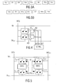
- Figure 3A is a schematic sectional representation of a pair of transmission lines which can be used in a switching matrix.
- the signals conveyed in optical transmissions are signals differential in phase opposition. That is, a signal line of one line transmission is actually made up of two parallel differential components for carry the differential signal.
- the principle of the matrix described with reference to the figures previous is kept, except that a signal channel actually consists of two channels parallel differentials.
- Each transmission line therefore has two channels differential S and Sq to transport the signal and a voltage reference channel or channel back Vcc.
- the total congestion resulting for a pair of successive differential transmission lines arranged according to FIG. 3A corresponds to 4 (A + B + B ') + 2A' + C.
- FIG. 3B illustrates a pair of differential transmission lines arranged according to the invention as illustrated, for example, in Figures 1 and 2.
- the same references are used to indicate the same elements.
- the voltage reference channel Vcc is common to the two successive differential transmission lines, which allows reduce the overall size of the two transmission lines. Indeed, using the same notations as for FIG. 3A, a total bulk of 4A + 2A '+ 3B + 4B', i.e. a reduction equal to B + C.
- the space saving achieved by the removal of a voltage reference channel per pair of transmission lines is estimated at minus about 10% of the space used according to each dimension of the matrix.
- FIG. 4 illustrates a part of a device according to a particular embodiment of the invention.
- Half of a complex cell 22 illustrated in FIG. 2 is represented in FIG. 4. This half corresponding to two interconnection points or basic cells C i, j and C i + 1, j associated with the same line of output transmission.
- a control member CTRL is provided for controlling the operation of the matrix by means of predetermined control signals according to said predefined switching plan.
- an output can only be connected to a single input by a single interconnection point placed in a first switching state, called active state, under the control of the control unit CTRL, all the others interconnection points capable of connecting other inputs to this same output being placed in a second switching state, called inactive state.
- Decoding means 43 are provided for decoding the control signals and deducing therefrom the switching state of the interconnection points.
- the decoding means 43 include local decoders associated with the interconnection points to perform local decoding of the control signals sent by the control member at the interconnection points.
- the control signals are binary signals and the decoders 43, binary decoders.
- the binary decoders 43 are connected to the control member by binary links distinct from the transmission lines to transport the binary control signals from the CTRL control member to the binary decoders 43.
- a pair of binary decoders DEC is associated with two pairs of interconnection points.
- the first pair of points comprises the points C i, j and C i + 1, j .
- the second pair has the points C i, j + 1 and C i + 1, j + 1 .
- each DEC decoder always has N inputs (not shown) but this time the binary decoders have 2 outputs for decoding the control signals received on the N binary links to the 2 interconnection points of each corresponding pair.
- Each decoder deduces therefrom a first result R1 j and R1 j + 1 , respectively, intended to control the first interconnection point of each pair.
- the decoders further include inverting means (not shown) for inverting the control signal on at least one of the N bit links with respect to the control signal used to provide the first result.
- Each decoder thus obtains a second result R2 j and R2 j + 1 , respectively, intended to control the second interconnection point of the corresponding pair.
- neither the control links nor the CTRL control member are shown in FIG. 5. These links are however present for each pair of interconnection points, between each DEC decoder associated with a pair of interconnection points and the CTRL control unit, as illustrated in Figure 4.
- FIG. 6 illustrates, purely by way of non-restrictive example, an embodiment of a DEC decoder represented in FIG. 5.
- the decoder comprises two stages of AND logic gates, denoted 61 to 63, for connecting 3 inputs, denoted b0 , b1 and b2, with two outputs, denoted S0 and S1.
- the 3 inputs b0, b1 and b2 are connected to the control device (not shown) via the N control links illustrated in Figure 4.
- the 2 outputs S0 and S1 are intended to provide the two binary control results , R1 j or R1 j + 1 on the one hand, and R2 j or R2 j + 1 on the other hand, to control a pair of interconnection points C i, j and C i + 1, j or C i, j + 1 and C i + 1, j + 1 , connectable, via a transmission line, to the same output of the switching matrix, O j or O j + 1 , according to the example illustrated in Figure 5.
- Two inputs b0 and b1 are connected to the input of a first AND gate 61 whose output is sent to the input of a second and third AND gate 62 and 63, respectively.
- the third input b2 is received at the input of the second AND gate 62 to provide, by performing a logical AND with the output of the first AND gate 61, a first command result R1 intended for the first interconnection point C i, j .
- Inversion means 65 are provided for inverting the signal received on the third input b2 and for supplying at the input of the third AND gate 63 said inverted signal with respect to the signal sent at the input of the second AND gate 62 and for deducing therefrom, by performing a logical AND with the output of the first AND gate 61, the second command result R2 intended for the second interconnection point C i + 1, j .
- FIGS. 4 to 6 which are not made to scale, such a DEC decoder with two outputs as illustrated in FIGS. 5 and 6 is less bulky than the sum of the two decoders 43 shown in Figure 4.
- FIGS. 1 to 6 can be incorporated in a integrated circuit, to be used, in particular, in a PABX of a network of telecommunications as shown in Figure 7.
- Figure 7 shows an example of digital telecommunications system according to the invention.
- the system includes a transmitter 71, receiver 72, automatic switch 73 comprising a device for switching of the type represented in FIGS. 1 to 5 and of the connections by optical fibers 75 to connect the transmitter 71 and the receiver 72 via the automatic exchange 73.
Landscapes
- Engineering & Computer Science (AREA)
- Computer Networks & Wireless Communication (AREA)
- Signal Processing (AREA)
- Use Of Switch Circuits For Exchanges And Methods Of Control Of Multiplex Exchanges (AREA)
- Data Exchanges In Wide-Area Networks (AREA)
Applications Claiming Priority (2)
| Application Number | Priority Date | Filing Date | Title |
|---|---|---|---|
| FR0115975 | 2001-12-11 | ||
| FR0115975A FR2833449A1 (fr) | 2001-12-11 | 2001-12-11 | Dispositif de commutation comportant une voie de reference en tension commune |
Publications (2)
| Publication Number | Publication Date |
|---|---|
| EP1320227A2 true EP1320227A2 (de) | 2003-06-18 |
| EP1320227A3 EP1320227A3 (de) | 2010-12-08 |
Family
ID=8870323
Family Applications (1)
| Application Number | Title | Priority Date | Filing Date |
|---|---|---|---|
| EP02080091A Withdrawn EP1320227A3 (de) | 2001-12-11 | 2002-12-05 | Schaltvorrichtung mit Referenzkanal auf gemeinsame Spannung |
Country Status (5)
| Country | Link |
|---|---|
| US (1) | US7245606B2 (de) |
| EP (1) | EP1320227A3 (de) |
| JP (1) | JP4087236B2 (de) |
| CN (1) | CN1314244C (de) |
| FR (1) | FR2833449A1 (de) |
Families Citing this family (2)
| Publication number | Priority date | Publication date | Assignee | Title |
|---|---|---|---|---|
| FR2833441A1 (fr) * | 2001-12-11 | 2003-06-13 | Koninkl Philips Electronics Nv | Dispositif de commutation comportant des moyens de decodage local |
| CN101621507B (zh) * | 2008-07-02 | 2012-06-13 | 鸿富锦精密工业(深圳)有限公司 | 双网物理隔离电路 |
Family Cites Families (10)
| Publication number | Priority date | Publication date | Assignee | Title |
|---|---|---|---|---|
| JPS56153832A (en) * | 1980-04-30 | 1981-11-28 | Nec Corp | Digital to analog converter |
| US4374384A (en) * | 1980-08-28 | 1983-02-15 | Westinghouse Electric Corp. | Matrix encoder for resistive sensor arrays |
| CA1254981A (en) * | 1986-02-18 | 1989-05-30 | Lester Kirkland | Communications switching system |
| USRE34444E (en) * | 1988-01-13 | 1993-11-16 | Xilinx, Inc. | Programmable logic device |
| AU9056391A (en) * | 1990-11-15 | 1992-06-11 | Nvision, Inc. | Switch composed of identical switch modules |
| EP0536964B1 (de) * | 1991-10-05 | 1998-03-18 | Fujitsu Limited | Aktive Flüssigkristall-Matrix-Anzeige mit verminderter Anzahl von Datenbusleitungen |
| JPH05199255A (ja) * | 1992-01-18 | 1993-08-06 | Mitsubishi Electric Corp | 電子クロスポイントスイッチ装置 |
| US5991296A (en) * | 1996-02-22 | 1999-11-23 | Fujitsu, Ltd. | Crossbar switch and method with reduced voltage swing and no internal blocking data path |
| JP3391374B2 (ja) * | 1998-12-25 | 2003-03-31 | 富士通株式会社 | クロスポイントスイッチ回路および基本スイッチセル電子回路 |
| FR2833441A1 (fr) * | 2001-12-11 | 2003-06-13 | Koninkl Philips Electronics Nv | Dispositif de commutation comportant des moyens de decodage local |
-
2001
- 2001-12-11 FR FR0115975A patent/FR2833449A1/fr not_active Withdrawn
-
2002
- 2002-12-05 EP EP02080091A patent/EP1320227A3/de not_active Withdrawn
- 2002-12-06 US US10/313,786 patent/US7245606B2/en not_active Expired - Fee Related
- 2002-12-06 JP JP2002355006A patent/JP4087236B2/ja not_active Expired - Fee Related
- 2002-12-06 CN CNB02154042XA patent/CN1314244C/zh not_active Expired - Fee Related
Also Published As
| Publication number | Publication date |
|---|---|
| US7245606B2 (en) | 2007-07-17 |
| EP1320227A3 (de) | 2010-12-08 |
| JP2003229885A (ja) | 2003-08-15 |
| CN1314244C (zh) | 2007-05-02 |
| CN1426205A (zh) | 2003-06-25 |
| US20030118032A1 (en) | 2003-06-26 |
| JP4087236B2 (ja) | 2008-05-21 |
| FR2833449A1 (fr) | 2003-06-13 |
Similar Documents
| Publication | Publication Date | Title |
|---|---|---|
| CA2235058C (fr) | Dispositif a ondes acoustiques de surface a couplage par proximite a entrees/sorties differentielles | |
| EP0711093A1 (de) | Vermittlungssystem für optische Pakete | |
| FR2735637A1 (fr) | Dispositif tout optique pour la regeneration d'un signal optique module selon un format rz | |
| EP3534536B1 (de) | Vorrichtung und photonisches verfahren zur umwandlung einer doppelbandfrequenz | |
| EP0497670B1 (de) | Optischer Konzentrator | |
| FR2768872A1 (fr) | Porte logique ou-exclusif a quatre entrees complementaires deux a deux et a deux sorties complementaires, et multiplieur de frequence l'incorporant | |
| EP1322076A1 (de) | Vermittlungsvorrichtung mit mitteln für lokale Dekodierung | |
| EP1320227A2 (de) | Schaltvorrichtung mit Referenzkanal auf gemeinsame Spannung | |
| EP1179964A2 (de) | Schalter für optische Signale | |
| FR2796766A1 (fr) | Amplificateur optique a pompage bidirectionnel | |
| EP1646262B1 (de) | Rekonfigurierbarer optischer Schalter | |
| EP1349417B1 (de) | Multicast-fähiger Crossconnect für optische Signale | |
| FR2830709A1 (fr) | Dispositif de commutation selective de frequences et circuit a retard optique reconfigurable l'incorporant | |
| FR2729040A1 (fr) | Matrice de commutation photonique | |
| FR2821504A1 (fr) | Dispositif d'extraction de frequence | |
| WO2003090392A1 (fr) | Dispositif optique et procédé pour convertir des signaux wdm en un signal otdm, et réciproquement | |
| FR2814305A1 (fr) | Dispositif de selection et de conversion de longueur d'onde, et matrice de commutation photonique l'incorporant | |
| FR2743965A1 (fr) | Procede et systeme de communication optique a routage passif | |
| EP0746070B1 (de) | Verfahren und Vorrichtung zur Kombination optischer Signale | |
| FR2864261A1 (fr) | Dispositif de regeneration d'un signal optique, utilisation d'un tel dispositif et installation comportant un tel dispositif | |
| EP1326473A1 (de) | Optische Schaltvorrichtung und Kontrolleverfahren dafür | |
| FR2813466A1 (fr) | Regenerateur tout-optique pour signaux multiplexes en longueur d'onde | |
| FR2811837A1 (fr) | Cellule elementaire de commutation optique et dispositifs comportant une telle cellule | |
| EP1207643A1 (de) | Vorrichtung zur Wellenlängenselektion und -Wandlung, und damit hergestellter optische Schaltmatrix | |
| EP1455551A2 (de) | Selektionsmodul für optische Schalter und optischer Schalter |
Legal Events
| Date | Code | Title | Description |
|---|---|---|---|
| PUAI | Public reference made under article 153(3) epc to a published international application that has entered the european phase |
Free format text: ORIGINAL CODE: 0009012 |
|
| AK | Designated contracting states |
Designated state(s): AT BE BG CH CY CZ DE DK EE ES FI FR GB GR IE IT LI LU MC NL PT SE SI SK TR |
|
| AX | Request for extension of the european patent |
Extension state: AL LT LV MK RO |
|
| RAP1 | Party data changed (applicant data changed or rights of an application transferred) |
Owner name: NXP B.V. |
|
| PUAL | Search report despatched |
Free format text: ORIGINAL CODE: 0009013 |
|
| AK | Designated contracting states |
Kind code of ref document: A3 Designated state(s): AT BE BG CH CY CZ DE DK EE ES FI FR GB GR IE IT LI LU MC NL PT SE SI SK TR |
|
| AX | Request for extension of the european patent |
Extension state: AL LT LV MK RO |
|
| AKY | No designation fees paid | ||
| REG | Reference to a national code |
Ref country code: DE Ref legal event code: R108 |
|
| REG | Reference to a national code |
Ref country code: DE Ref legal event code: R108 Effective date: 20110822 |
|
| STAA | Information on the status of an ep patent application or granted ep patent |
Free format text: STATUS: THE APPLICATION IS DEEMED TO BE WITHDRAWN |
|
| 18D | Application deemed to be withdrawn |
Effective date: 20110609 |