EP1326337A1 - Standard-CMOS-Hochspannungs-Gegentakttreiber - Google Patents
Standard-CMOS-Hochspannungs-Gegentakttreiber Download PDFInfo
- Publication number
- EP1326337A1 EP1326337A1 EP02368002A EP02368002A EP1326337A1 EP 1326337 A1 EP1326337 A1 EP 1326337A1 EP 02368002 A EP02368002 A EP 02368002A EP 02368002 A EP02368002 A EP 02368002A EP 1326337 A1 EP1326337 A1 EP 1326337A1
- Authority
- EP
- European Patent Office
- Prior art keywords
- gate
- coupled
- pfet
- drain
- source
- Prior art date
- Legal status (The legal status is an assumption and is not a legal conclusion. Google has not performed a legal analysis and makes no representation as to the accuracy of the status listed.)
- Granted
Links
- 239000003990 capacitor Substances 0.000 claims description 13
- 210000004027 cell Anatomy 0.000 description 28
- 230000015556 catabolic process Effects 0.000 description 8
- 238000000034 method Methods 0.000 description 6
- 238000009792 diffusion process Methods 0.000 description 3
- 229910021420 polycrystalline silicon Inorganic materials 0.000 description 3
- 229920005591 polysilicon Polymers 0.000 description 3
- 230000003068 static effect Effects 0.000 description 2
- 210000003850 cellular structure Anatomy 0.000 description 1
- 239000000463 material Substances 0.000 description 1
- 230000001105 regulatory effect Effects 0.000 description 1
- 230000001052 transient effect Effects 0.000 description 1
Images




Classifications
-
- H—ELECTRICITY
- H03—ELECTRONIC CIRCUITRY
- H03K—PULSE TECHNIQUE
- H03K19/00—Logic circuits, i.e. having at least two inputs acting on one output; Inverting circuits
- H03K19/003—Modifications for increasing the reliability for protection
- H03K19/00315—Modifications for increasing the reliability for protection in field-effect transistor circuits
-
- H—ELECTRICITY
- H03—ELECTRONIC CIRCUITRY
- H03K—PULSE TECHNIQUE
- H03K17/00—Electronic switching or gating, i.e. not by contact-making and –breaking
- H03K17/10—Modifications for increasing the maximum permissible switched voltage
- H03K17/102—Modifications for increasing the maximum permissible switched voltage in field-effect transistor switches
Definitions
- the invention relates to a push-pull driver, and more particularly, to a high voltage, push-pull driver circuit compatible with standard CMOS devices.
- Input and output drivers are an especially challenging part of application specific integrated circuit (ASIC) design in advanced CMOS process.
- Advanced CMOS processes use very small device design rules, including shallow junctions and thin gate oxides.
- the internal voltage of the IC device is reduced to avoid voltage breakdown.
- external signals may be exposed to high voltage transient conditions. Therefore, the IC circuits that interface between the internal and external voltage levels are especially difficult to achieve.
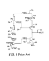
- a push-pull driver output is formed.
- a switch P1 22 is provided to pull the output, OUT 10, to the upper rail voltage, VCC 26.
- a switch N1 14 is also provided to push OUT 10 to the lower rail, or ground, VSS 30.
- the output switches, P1 22 and N1 14 are controlled such that only one switch is ON at any given time.
- the pull up driver may also be called a high side driver.
- the push down driver may also be called a low side driver.
- the VCC 26 level is biased to a relatively high voltage compared to the internal VDD 50 voltage. For example, while the VDD 50 level is about 3 Volts, the VCC 26 is about 10 Volts.
- the low voltage PFET devices, P1 22 and P2 18, are arranged in a cascade.
- the top PFET P1 22 has the gate terminal tied to the PFET switching signal, SWP 56, and is the switching device.
- the bottom PFET P2 18 is always biased ON.
- P1 22 and P2 18 are formed in separate n-wells and have source and bulk coupled.
- the voltage divider, R1 38 and R2 42 divides VCC 26 in half to create VCC/2 34.
- the cascade arrangement and gate bias on P2 18 allows the low voltage PFET devices, P1 22 and P2 18, to effectively high side switch the VCC voltage 26 onto OUT 10.
- the arrangement suffers the disadvantage of a very limited VCC upper range. This is because this cascade structure cannot be effectively extended to greater than two cascaded devices without creating a sophisticated biasing circuit. It is essential that each PFET device in the cascade stack have a carefully regulated gate voltage so that gate oxide or gate-induced avalanche breakdown or drain-to-source punch through does not occur. Unfortunately, the cascade bias voltage cannot respond to changes in the output voltage.
- the example push down, or low side driver, switch N1 14 suffers the disadvantage of insufficient gate drive.
- the NFET switching signal, SWN 58 is generated by the low voltage logic 46 that swings from VDD 50 to VSS 30. Therefore, the output NFET, N1 14, only has about a 3 Volt gate drive. To achieve a low impedance output, a very large NFET must be used. This costs a great amount of chip area.
- U.S. Patent 6,081,132 to Isbara describes a push-pull CMOS driver with a cascaded PMOS section. The gate voltage of the cascaded devices is controlled using a biasing circuit.
- U.S. Patent 6,157,223 to Blake teaches a push-pull CMOS driver with a cascaded PMOS section. The output voltage is fed back for gate biasing.
- a principal object of the present invention is to provide an effective and very manufacturable high voltage, push-pull driver circuit.
- a further object of the present invention is to provide a high voltage, push-pull driver that is compatible with standard CMOS.
- a still further object of the present invention is to provide a high voltage, pull-up, or high side, driver using low voltage capable PFET devices.
- a yet still further object of the present invention is to protect low voltage PFET devices by cascading devices.
- Another yet still further object of the present invention is to protect the gate terminals of the PFET devices by limiting the gate voltage using a resistor network
- Another yet still further object of the present invention is to enhance the ESD capability by providing gate resistance, gate-to-source capacitance, and gate-to-drain capacitance on each of the cascaded FET devices.
- Another yet still further object of the present invention is to insure the ON state of the PFET devices by limiting the gate voltage using a diode network.
- a still further object of the present invention is to provide a high voltage, push, or low side, driver .
- a yet still further object of the present invention is to provide a boosted gate drive to reduce the ON resistance of a NFET output.
- a new high voltage, high side driver circuit has been achieved.
- the circuit comprises, first, a top PFET having gate, drain, source, and bulk.
- the gate is coupled to a switching signal.
- the source is coupled to a high voltage.
- a top resistor has first and second terminals.
- the first terminal is coupled to the high voltage.
- a middle PFET cell comprises, first, a middle PFET having gate, drain, source, and bulk.
- the source is coupled to the top PFET drain.
- the gate is coupled to the top resistor second terminal.
- a middle resistor has first and second terminals.
- the first terminal is coupled to the middle PFET gate.
- a middle means of clamping said middle PFET gate to a clamping voltage completes the middle PFET cell.
- a bottom PFET cell comprises, first, a bottom PFET having gate, drain, source, and bulk. The gate is coupled to the middle resistor second terminal, the source is coupled to the middle PFET drain, and the drain forms a high side driver output. A bottom resistor is coupled between the bottom PFET gate and the high side driver output. Finally, a bottom means of clamping said bottom PFET gate to a clamping voltage completes the bottom PFET cell.
- the means of clamping may be a diode or a bipolar transistor.
- a new high voltage, low side driver circuit comprises, first, an output NFET having gate, drain, and source.
- the source is coupled to ground, and the drain forms a low side driver output.
- a low voltage control means has an input and an output. The input and output voltages vary between ground and a low voltage.
- a diode is coupled between the low voltage control means output and the output NFET gate.
- a current mirror is coupled to the output NFET gate to pull the output NFET gate to a drive voltage above said low voltage to thereby reduce the ON resistance of the output NFET.
- the current mirror current is proportional to the output NFET drain current.
- the current mirror is switched OFF when the output NFET is OFF.
- the diode blocks the drive voltage from the low voltage control means.
- a new high voltage, low side driver circuit comprises, first, a bottom NFET having gate, drain, source, and bulk. The gate is coupled to a switching signal, and the source is coupled to ground.
- a bottom resistor has first and second terminals. The first terminal is coupled to ground.
- a middle NFET cell comprises a middle NFET having gate, drain, source, and bulk. The source is coupled to the bottom NFET drain, and the gate is coupled to the bottom resistor second terminal.
- a middle resistor has first and second terminals. The first terminal is coupled to the middle NFET gate.
- a middle means of clamping the middle NFET gate to a clamping voltage completes the middle cell.
- a top NFET cell comprises, first, a top NFET having gate, drain, source, and bulk.
- the gate is coupled to the middle resistor second terminal, the source is coupled to the middle NFET drain, and the drain forms a low side driver output.
- a top resistor is coupled between the top NFET gate and the low side driver output.
- the preferred embodiments disclose a high side driver and a low side driver circuits with improved high voltage performance. These high side and low side drivers may be combined in a single application to create a push-pull output circuit. Alternatively, the high side and low side driver circuits may be used independently. It should be clear to those experienced in the art that the present invention can be applied and extended without deviating from the scope of the present invention.
- FIG. 2A a first preferred embodiment of the present invention high side driver is illustrated.
- a three PFET cascade stage is used.
- the novel configuration may be extended to greater than three PFET devices.
- the high side driver is designed for switching a high voltage, VCC 104, relative to the logic low voltage, onto the output, OUT 100.
- a top PFET 116 has gate, drain, and source. The gate is coupled to a switching signal, SWP 108. SWP 108 switches between VCC level and a lower voltage below the threshold of P1 116. The source of P1 116 is coupled to VCC.
- a top resistor, RT 128, has first and second terminals. The first terminal is coupled to VCC.
- a middle PFET cell comprises a PFET, PM 120, a resistor, RM 132, and a means of clamping DM 140 the middle PFET PM 120 gate to a clamping voltage V CLAMP 112.
- the means of clamping comprises a diode, DM 140.
- the middle cell PFET PM 120 has gate, drain, source, and bulk.
- the PM 120 source is coupled to the top PFET PT 116 drain.
- the PM 120 gate is coupled to the second terminal of RT 128.
- the middle cell resistor RM 132 has first and second terminals.
- the RM 132 first terminal is coupled to the PM 120 gate.
- the middle cell diode DM 140 is coupled between the PM 120 gate and a clamping voltage, V CLAMP 112.
- a bottom PFET cell comprises a PFET, PB 124, a resistor, RB 136, and a means of clamping DB 144 the gate of PB 124 to the clamping voltage V CLAMP 112.
- the means of clamping preferably comprises a diode, DB 144.
- the bottom cell PFET, PB 124 has gate, drain, and source.
- the PB 124 gate is coupled to the middle cell resistor, RM 132, second terminal.
- the PB 124 source is coupled to the middle cell PFET, PM 120, drain.
- the PB 124 drain forms the high side driver output, OUT 100.
- the bottom cell resistor, RB 136 is coupled between the PB 124 gate and OUT 100.
- the bottom cell diode, DB 144 is coupled between the PB 124 gate and the clamping voltage, V CLAMP 112.
- Resistors RT 128, RM 132, and RB 136 form a divider that optimally protects the PFET devices, 120 and 124, from large voltage differences between VCC and OUT.
- the voltage divider provides for variable voltage biasing on the gates of PM 120 and PB 124 that responds to changes in potential from VCC to OUT as the high side driver switches from the OFF state to the ON state. For example, if the VCC voltage is nominally about 15 Volts, then the voltage drop across the cascade stack is about 15 Volts if OUT 100 is at about 0 Volts. It is necessary that the gates of PM 120 and PB 124 be biased so that these devices are always in the ON state. It is also important that the gate-to-source voltage and the gate-to-drain voltage of PM 120 and PB 124 not be so large that breakdown occurs.
- PM 120 and PB 124 are formed in separate n-well regions. Further, it is preferred that the source and bulk (n-well) of PM 120 are coupled. The source and bulk of PB 124 should also be coupled. If the drain-to-source breakdown voltage of PT, PM, and PB is much lower than the gate-to-source breakdown, then one or more of transistors PT, PM, and PB can be located in the same well.
- RB 136 provides a feedback path for the OUT 100 voltage so that the gate biases on PM 120 and PB 124 will automatically track the OUT voltage.
- the resistor divider, RT 128, RM 132, and RB 136 may comprise resistors formed as diffusion regions, polysilicon resistors, or diode-connected PFET devices.
- the presence of the means of clamping, DM 140 and DB 144, provides an absolute upper limit on the gate voltages of PM 120 and PB 124.
- the gate voltages are clamped to one diode drop (about 0.7 Volts) above the clamping voltage, V CLAMP 112.
- the clamping diodes insure that PM 120 and PB 124 remain ON even when the OUT voltage is nearly at the VCC level.
- the clamping voltage, V CLAMP 112 is less than VCC and may be between about 4 Volts and 6 Volts below VCC where VCC is about 15 Volts.
- the novel high side driver circuit can work with a VCC 104 voltage of up to about 3 times the standard supply voltage because of the novel method of biasing the cascade transistors.
- a second preferred embodiment of the present invention high side driver is illustrated where gate resistors, gate-to-drain capacitors, and gate-to-source capacitors are added to improve ESD performance.
- the principle of the novel biasing of the cascaded transistors is extended by adding series gate resistance RTG 160, RMG 162, and RBG 164 to each of the cascaded transistors PT 116, PM 120, and PB 124, respectively.
- small gate-to-source and gate-to-drain capacitors are added to each of the cascaded transistors.
- gate-to-source capacitors CT1 166, CM1 172, and CB1 176 are added to cascaded transistors PT 116, PM 120, and PB 124, respectively.
- Gate-to-drain capacitors CT2 168, CM2 174, and CB2 178 are added to cascaded transistors PT 116, PM 120, and PB 124, respectively.
- the presence of the gate resistors, the gate-to-drain capacitors, and the gate-to-source capacitors improves the ESD performance of the novel circuit.
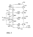
- a third preferred embodiment structure with a four PFET stack is illustrated. More than four PFET devices may be stacked with each additional PFET cell added as shown in Fig. 3. Additional PFET devices extend the useful operating voltage on the VCC.
- the middle cell components illustrated in Fig. 2 as PM, RM, and DM are duplicated. Therefore, two middle cells are used in the cascade of Fig. 3. The first middle cell uses PM1 220, RM1 236, and DM1 244. The second middle cell uses PM2 224, RM2 240, and DM2 248. Note that each of the middle cells and the bottom cell are still clamped to the V CLAMP 212 voltage. In this configuration, the VCC 204 operating range can be extended to about four times the standard supply voltage.
- a first preferred embodiment of a switching circuit and a clamping voltage generator for the high side driver of the present invention is illustrated.
- the switching signal, SWP 380 is generated using the switched resistor divider comprising RS1 352, RS2 356, and NS 360.
- RS1 352 is coupled between VCC 304 and RS2 356.
- RS 2 356 is coupled between RS1 352 and the drain of NFET NS 360.
- SWP 380 is pulled to the VCC voltage by RS1 352.
- SWP 380 is driven to a fraction of VCC determined by the ratio of RS1 and RS2.
- the asserted voltage SWP 380 can be selected to insure that the gate of PT 312 does not receive too low of a voltage and create a gate oxide breakdown condition. Since NS 360 is OFF when PT 312 is OFF, there is no static current draw in the resistor divider during the OFF state.
- the clamping voltage, V CLAMP 376 is also preferably generated using a switched voltage divider comprising RC1 340, RC2 344, and NC 348.
- the purpose of V CLAMP 376 is to provide a voltage limit for the gates of the cascaded PFET devices PM 316 and PB 320 such that the gate voltages on PM and PB do not reach VCC.
- the worst case condition occurs when PT 312 is ON and OUT 300 is pulled high. In this condition, a small voltage drop occurs across the resistor divider comprising RT 324, RM 328, and RB 330. Therefore, the gates of PM and PB will be pulled up to nearly the VCC voltage by the resistor divider.
- the resistors for the switching circuit and for the clamping voltage circuit, RS1 352, RS1 356, RC1 340, and RC2 344, may comprise doped or undoped polysilicon resistors, diffusion resistors, or diode-coupled PFET devices.
- Fig. 4B illustrates a second preferred embodiment of a clamping voltage generator having lowered impedance.
- the resistor values of RC1 340 and RC2 344 in the circuit of Fig. 4A cannot be very large.
- bipolar transistors are used as the means of clamping instead of the diodes, then the values of the resistors in the divider can be made large.
- bipolar p-n-p transistors QM 393 and QB 394 are used as the means of clamping. More specifically, the middle bipolar transistor QM 393 has emitter coupled to the gate of the middle PFET PM 316, base coupled to the clamping voltage 396, and collector coupled to ground VSS 308.
- the bottom bipolar transistor QB 393 has emitter coupled to the gate of the bottom PFET PM 316, base coupled to the clamping voltage 397, and collector coupled to ground VSS 308.
- Fig. 4C illustrates a first preferred embodiment of the present invention, low side driver with an improved NFET cascade structure.
- the principle of cascading the transistors using a novel biasing scheme is applied to a low side driver using cascaded NMOS devices.
- This structure is preferably used in processes where isolated NMOS transistors are available, such as in p-well processes or triple-well processes.
- the circuit comprises, first, a bottom NFET NB 624 having gate, drain, source, and bulk.
- the gate is coupled to a switching signal SWN 612, and the source is coupled to ground VSS 608.
- a bottom resistor RB 636 has first and second terminals. The first terminal is coupled to ground VSS.
- a middle NFET cell comprises a middle NFET NM 620 having gate, drain, source, and bulk.
- the source of NM is coupled to the bottom NFET NB 624 drain, and the gate of NM is coupled to the bottom resistor RB second terminal at node VM 660.
- a middle resistor RM 632 has first and second terminals. The first terminal of RM is coupled to the middle NFET NM gate.
- a middle means of clamping DB 644 the middle NFET NM 620 gate to a clamping voltage V CLAMP 664 completes the middle cell.
- a top NFET cell comprises, first, a top NFET NT 616 having gate, drain, source, and bulk. The gate of NT is coupled to the middle resistor RM second terminal at node VT 656. The source of NT is coupled to the middle NFET NM drain. The drain of NT forms a low side driver output OUT 600. A top resistor RT 628 is coupled between the top NFET NT gate and the low side driver output OUT.
- a top means of clamping DM 640 the top NFET NT gate to the clamping voltage V CLAMP 664 completes the top NFET cell.
- the low side drive circuit can be combined with a high side drive circuit to form a push-pull output.
- each of the NFET devices, NB, NM, and NT be formed in a separate well.
- the bulk and source should be coupled. If the source-to-drain breakdown voltage of the NFET devices is lower than the gate-to-source breakdown voltage, then the devices can be formed in common wells without loss of high voltage performance.
- gate resistance, gate-to-source capacitance, and gate-to-drain capacitance can be added to each of the cascaded NFET transistors to further improve ESD performance of the circuit.
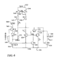
- a second embodiment of the present invention illustrates a low side driver.
- the high side driver of the first embodiment may be combined with the low side driver of the second embodiment to create a high voltage, push-pull output driver.
- the output, OUT 400 is driven by an NFET, ND 416 having gate, drain, and source.
- the ND 416 source is coupled to ground, while the drain forms the low side driver output.
- ND 416 is controlled by a low voltage control means 424 having an input, LVSWNB 436, and an output, LVSWN 438.
- LVSWNB 436 and LVSWN 438 voltages vary between ground and the logic low voltage, VDD 408.
- a diode, DN 420 is coupled between the low voltage control means output, LVSWN 438, and the gate of ND 416 at the node SWN 432.
- a current mirror 428 is coupled to the gate of ND 416 to pull the gate to a drive voltage above VDD when ND 416 is ON.
- the ON resistance of the ND 416 is reduced due to the increased gate drive.
- the current mirror 428 current is proportional to the ND 416 drain current.
- the current mirror 428 is switched OFF when the ND is OFF.
- the diode, DN 420 blocks the higher drive voltage from the low voltage control means 424.
- the current mirror circuit preferably comprises a lower mirror and an upper mirror.
- the lower mirror comprises NFET devices, N1 520, N2 524, N3 532, and N4 528.
- the upper mirror comprises PFET devices, P1 544 and P2 548, and resistors, R1 540 and R2 552.
- the lower mirror comprises, first, N1 520 having gate, drain, and source.
- the source is coupled to ground, or VSS 504, and the drain is coupled to the output ND 516 drain.
- N2 524 has gate, drain, and source. The gate is coupled to the gate of N1 520 to form the circuit node NB, or NBIAS.
- the source of N2 524 is coupled to ground 504.
- N3 532 has gate, drain, and source.
- the source of N3 532 is coupled to NB 536.
- the drain of N3 532 is coupled to the drain of ND 516.
- the gate of N3 is coupled to the gate of ND 516.
- N4 528 has gate, drain, and source.
- the source of N4 is coupled to ground.
- the drain of N4 is coupled to NB 536, and the gate is coupled to LVSWNB 568.
- the upper mirror comprises P1 544 having gate, drain, and source.
- the source of P1 544 is coupled to the high voltage, or VCC 512.
- the gate and drain of P1 are coupled together.
- Resistor R1 540 is coupled between the drain of P1 544 and the drain of N2 524.
- PFET P2 548 has gate, drain, and source.
- the source of P2 548 is coupled to VCC 512 and the gate is coupled to the gate of P1 544 to form the PB 546, or PBIAS, node.
- Resistor R2 552 is coupled between the drain of P2 548 and the gate of the output NFET ND 516.
- VDD 568 When LVSWNB 568 is low, the inverter formed by low voltage PFET PLV 560 and low voltage NFET 556 drives SWN 572 to the low voltage supply, VDD 508. Since VDD 508 may be at about 3 Volts, the available gate drive for ND 516 is limited. However, now N3 532 is ON and N4 528 is OFF. N3 connects NB 536 to OUT 500 and establishes the lower current mirror. N1 will conduct drain current, I 1 , in proportion to the output current, I OUT . Therefore, since N2 524 is commonly biased with N1 520 by node NB, current I 2 will mirror current I 1 .
- the lower current mirror current, I 2 creates the upper current mirror current, I 3 .
- This current causes the SWN 572 voltage to rise and creates a larger gate drive on ND 516. Note that, due to R2 552, SWN 572 does not rise all the way to near VCC. This is important because the ND 516 may not be capable of sustaining a gate voltage at the VCC 512 voltage.
- the diode, DN 564 protects PLV 560 from the larger voltage on SWN 572.
- diode DN 564 may be formed by tying the bulk of PLV 560 to a voltage above VDD 508 during the output ON state.
- the upper mirror resistors R1 540 and R2 552 may be formed as diffusion resistors, doped or undoped polysilicon resistors, or diode-connected PFET devices to limit the drain-to-source voltage of P1 and P2, NLV and N2.
- the novel configuration of the second preferred embodiment allows the drive voltage to exceed VDD 508 by between about 1 Volts and 3 Volts where VDD is about 3 Volts and the maximum gate-to-source voltage of ND 516 is about 6 Volts. Higher voltage boost is possible and depends on scaling of current mirrors P1/P2 and N1/N2.
- the present invention provides a unique and advantageous high voltage, push-pull output driver that is compatible with standard CMOS.
- the unique cascade biasing configuration facilitates a multiple transistor PFET cascade.
- the unique gate drive circuit for the NFET provides additional gate drive above the low voltage level.
- the advantages of the present invention may now be summarized.
- Second, the high voltage, push-pull driver is compatible with standard CMOS.
- Third, the high voltage, pull-up, or high side, driver uses low voltage capable PFET devices formed by cascading devices.
- Fourth, the PFET devices are prevented from breaking down by limiting the gate voltage using a resistor network.
- the ON state of the PFET devices is insured by a diode network to a clamping voltage.
- a high voltage, push, or low side, driver is achieved using an NFET device.
- a boosted gate drive is provided to reduce the ON resistance of the NFET output.
- the low voltage control circuit is protected from the drive voltage by a diode.
- the novel current sense circuit provides an effective and manufacturable alternative to the prior art.
Landscapes
- Physics & Mathematics (AREA)
- Engineering & Computer Science (AREA)
- Computer Hardware Design (AREA)
- Computing Systems (AREA)
- General Engineering & Computer Science (AREA)
- Mathematical Physics (AREA)
- Logic Circuits (AREA)
- Electronic Switches (AREA)
- Metal-Oxide And Bipolar Metal-Oxide Semiconductor Integrated Circuits (AREA)
- Semiconductor Integrated Circuits (AREA)
- Junction Field-Effect Transistors (AREA)
Priority Applications (6)
| Application Number | Priority Date | Filing Date | Title |
|---|---|---|---|
| ES02368002T ES2307715T3 (es) | 2002-01-03 | 2002-01-03 | Excitador push-pull de alta tension de cmos estandar. |
| EP02368002A EP1326337B1 (de) | 2002-01-03 | 2002-01-03 | Standard-CMOS-Hochspannungs-Gegentakttreiber |
| PT02368002T PT1326337E (pt) | 2002-01-03 | 2002-01-03 | Excitador simétrico de alta tensão em cmos standard |
| AT02368002T ATE397322T1 (de) | 2002-01-03 | 2002-01-03 | Standard-cmos-hochspannungs-gegentakttreiber |
| DE60226835T DE60226835D1 (de) | 2002-01-03 | 2002-01-03 | Standard-CMOS-Hochspannungs-Gegentakttreiber |
| US10/043,748 US6573752B1 (en) | 2002-01-03 | 2002-01-10 | High voltage push-pull driver on standard CMOS |
Applications Claiming Priority (1)
| Application Number | Priority Date | Filing Date | Title |
|---|---|---|---|
| EP02368002A EP1326337B1 (de) | 2002-01-03 | 2002-01-03 | Standard-CMOS-Hochspannungs-Gegentakttreiber |
Publications (2)
| Publication Number | Publication Date |
|---|---|
| EP1326337A1 true EP1326337A1 (de) | 2003-07-09 |
| EP1326337B1 EP1326337B1 (de) | 2008-05-28 |
Family
ID=8185765
Family Applications (1)
| Application Number | Title | Priority Date | Filing Date |
|---|---|---|---|
| EP02368002A Expired - Lifetime EP1326337B1 (de) | 2002-01-03 | 2002-01-03 | Standard-CMOS-Hochspannungs-Gegentakttreiber |
Country Status (6)
| Country | Link |
|---|---|
| US (1) | US6573752B1 (de) |
| EP (1) | EP1326337B1 (de) |
| AT (1) | ATE397322T1 (de) |
| DE (1) | DE60226835D1 (de) |
| ES (1) | ES2307715T3 (de) |
| PT (1) | PT1326337E (de) |
Cited By (2)
| Publication number | Priority date | Publication date | Assignee | Title |
|---|---|---|---|---|
| DE102004019345A1 (de) * | 2004-04-21 | 2005-11-17 | Austriamicrosystems Ag | Ausgangsstufenanordnung |
| CN108365737A (zh) * | 2017-01-25 | 2018-08-03 | 奕力科技股份有限公司 | 高压电源装置 |
Families Citing this family (13)
| Publication number | Priority date | Publication date | Assignee | Title |
|---|---|---|---|---|
| US20050275027A1 (en) * | 2003-09-09 | 2005-12-15 | Micrel, Incorporated | ESD protection for integrated circuits |
| TW200638679A (en) * | 2005-04-28 | 2006-11-01 | Sunplus Technology Co Ltd | Logic gate device with low electromagnetic interference |
| US7485984B2 (en) * | 2006-05-12 | 2009-02-03 | Delphi Technologies, Inc. | Control module |
| US8026745B2 (en) | 2009-03-16 | 2011-09-27 | Apple Inc. | Input/output driver with controlled transistor voltages |
| US9331865B2 (en) * | 2013-12-03 | 2016-05-03 | Nxp B.V. | Comparator circuit |
| US9831764B2 (en) * | 2014-11-20 | 2017-11-28 | Stmicroelectronics International N.V. | Scalable protection voltage generator |
| DE102016111641A1 (de) | 2016-06-24 | 2017-12-28 | Infineon Technologies Ag | Schalter |
| EP3352042B1 (de) * | 2017-01-18 | 2021-04-07 | ams AG | Ausgangsschaltung und verfahren zur bereitstellung eines ausgangsstroms |
| US10095329B1 (en) | 2017-03-28 | 2018-10-09 | Microsoft Technology Licensing, Llc | Discrete high impedance implementation on push-pull outputs |
| EP3855295A1 (de) | 2020-01-24 | 2021-07-28 | Microsoft Technology Licensing, LLC | Treiberschaltung und verfahren zur ansteuerung einer kapazitiven last |
| US11502674B2 (en) * | 2020-07-20 | 2022-11-15 | Texas Instruments Incorporated | Optimized low Ron flatness gate driver |
| US12132473B2 (en) | 2023-03-13 | 2024-10-29 | Nxp Usa, Inc. | Switch with cascode arrangement |
| US12126338B1 (en) * | 2023-04-04 | 2024-10-22 | Nxp Usa, Inc. | Switch with cascode arrangement |
Citations (3)
| Publication number | Priority date | Publication date | Assignee | Title |
|---|---|---|---|---|
| US4751408A (en) * | 1985-09-06 | 1988-06-14 | Thomson-Csf | Voltage-switching device |
| US4906904A (en) * | 1989-06-27 | 1990-03-06 | Digital Equipment Corporation | Cathode ray tube deflection circuit with solid state switch |
| DE4428548A1 (de) * | 1994-08-12 | 1996-02-15 | Bosch Gmbh Robert | Schaltungsanordnung mit einem Feldeffekttransistor |
Family Cites Families (4)
| Publication number | Priority date | Publication date | Assignee | Title |
|---|---|---|---|---|
| US6005415A (en) * | 1997-07-18 | 1999-12-21 | International Business Machines Corporation | Switching circuit for large voltages |
| US6157223A (en) | 1997-12-23 | 2000-12-05 | Texas Instruments Incorporated | Output buffer with switching PMOS drivers |
| US6081132A (en) | 1998-03-09 | 2000-06-27 | Intel Corporation | High voltage drive output buffer for low Voltage integrated circuits |
| US6396326B1 (en) * | 2000-06-30 | 2002-05-28 | Intel Corporation | High voltage driver having overshoot/undershoot protection circuitry |
-
2002
- 2002-01-03 AT AT02368002T patent/ATE397322T1/de active
- 2002-01-03 EP EP02368002A patent/EP1326337B1/de not_active Expired - Lifetime
- 2002-01-03 PT PT02368002T patent/PT1326337E/pt unknown
- 2002-01-03 DE DE60226835T patent/DE60226835D1/de not_active Expired - Lifetime
- 2002-01-03 ES ES02368002T patent/ES2307715T3/es not_active Expired - Lifetime
- 2002-01-10 US US10/043,748 patent/US6573752B1/en not_active Expired - Lifetime
Patent Citations (3)
| Publication number | Priority date | Publication date | Assignee | Title |
|---|---|---|---|---|
| US4751408A (en) * | 1985-09-06 | 1988-06-14 | Thomson-Csf | Voltage-switching device |
| US4906904A (en) * | 1989-06-27 | 1990-03-06 | Digital Equipment Corporation | Cathode ray tube deflection circuit with solid state switch |
| DE4428548A1 (de) * | 1994-08-12 | 1996-02-15 | Bosch Gmbh Robert | Schaltungsanordnung mit einem Feldeffekttransistor |
Cited By (5)
| Publication number | Priority date | Publication date | Assignee | Title |
|---|---|---|---|---|
| DE102004019345A1 (de) * | 2004-04-21 | 2005-11-17 | Austriamicrosystems Ag | Ausgangsstufenanordnung |
| DE102004019345B4 (de) * | 2004-04-21 | 2007-02-08 | Austriamicrosystems Ag | Ausgangsstufenanordnung |
| US8063689B2 (en) | 2004-04-21 | 2011-11-22 | Austriamicrosystems Ag | Output stage system |
| CN108365737A (zh) * | 2017-01-25 | 2018-08-03 | 奕力科技股份有限公司 | 高压电源装置 |
| CN108365737B (zh) * | 2017-01-25 | 2020-03-31 | 奕力科技股份有限公司 | 高压电源装置 |
Also Published As
| Publication number | Publication date |
|---|---|
| PT1326337E (pt) | 2008-09-08 |
| ATE397322T1 (de) | 2008-06-15 |
| US6573752B1 (en) | 2003-06-03 |
| ES2307715T3 (es) | 2008-12-01 |
| EP1326337B1 (de) | 2008-05-28 |
| DE60226835D1 (de) | 2008-07-10 |
Similar Documents
| Publication | Publication Date | Title |
|---|---|---|
| US5635861A (en) | Off chip driver circuit | |
| US7071730B2 (en) | Voltage level translator circuitry | |
| US5528190A (en) | CMOS input voltage clamp | |
| EP1326337B1 (de) | Standard-CMOS-Hochspannungs-Gegentakttreiber | |
| US6031394A (en) | Low voltage CMOS circuit for on/off chip drive at high voltage | |
| JPH07118644B2 (ja) | オフ・チップ・ドライバ回路 | |
| US6741098B2 (en) | High speed semiconductor circuit having low power consumption | |
| US5990705A (en) | CMOS I/O circuit with high-voltage input tolerance | |
| US7429873B2 (en) | High voltage digital driver with dynamically biased cascode transistors | |
| US6600361B2 (en) | Semiconductor device | |
| US5793592A (en) | Dynamic dielectric protection circuit for a receiver | |
| EP0630110B1 (de) | Pegelumsetzungsschaltung | |
| KR100238499B1 (ko) | 시모스(cmos) 버퍼회로 | |
| US20020050855A1 (en) | Semiconductor device | |
| US6496054B1 (en) | Control signal generator for an overvoltage-tolerant interface circuit on a low voltage process | |
| JPH10173499A (ja) | 出力ドライバ回路及び半導体装置 | |
| GB1595143A (en) | Fet inverter circuits | |
| US20030067042A1 (en) | Stacked NMOS device biasing on MOS integrated circuits and methods therefor | |
| US7236002B2 (en) | Digital CMOS-input with N-channel extended drain transistor for high-voltage protection | |
| US5592010A (en) | Semiconductor device | |
| US5170078A (en) | Highly stable high-voltage output buffer using CMOS technology | |
| US5187386A (en) | Low standby current intermediate dc voltage generator | |
| US6236235B1 (en) | Output circuit | |
| US7402869B2 (en) | Apparatus and method for breakdown protection of a source follower circuit | |
| US5426377A (en) | BiMIS circuit |
Legal Events
| Date | Code | Title | Description |
|---|---|---|---|
| PUAI | Public reference made under article 153(3) epc to a published international application that has entered the european phase |
Free format text: ORIGINAL CODE: 0009012 |
|
| AK | Designated contracting states |
Designated state(s): AT BE CH CY DE DK ES FI FR GB GR IE IT LI LU MC NL PT SE TR |
|
| AX | Request for extension of the european patent |
Extension state: AL LT LV MK RO SI |
|
| 17P | Request for examination filed |
Effective date: 20040107 |
|
| AKX | Designation fees paid |
Designated state(s): AT BE CH CY DE DK ES FI FR GB GR IE IT LI LU MC NL PT SE TR |
|
| 17Q | First examination report despatched |
Effective date: 20070226 |
|
| GRAP | Despatch of communication of intention to grant a patent |
Free format text: ORIGINAL CODE: EPIDOSNIGR1 |
|
| GRAS | Grant fee paid |
Free format text: ORIGINAL CODE: EPIDOSNIGR3 |
|
| GRAA | (expected) grant |
Free format text: ORIGINAL CODE: 0009210 |
|
| AK | Designated contracting states |
Kind code of ref document: B1 Designated state(s): AT BE CH CY DE DK ES FI FR GB GR IE IT LI LU MC NL PT SE TR |
|
| REG | Reference to a national code |
Ref country code: GB Ref legal event code: FG4D |
|
| REG | Reference to a national code |
Ref country code: CH Ref legal event code: EP |
|
| REF | Corresponds to: |
Ref document number: 60226835 Country of ref document: DE Date of ref document: 20080710 Kind code of ref document: P |
|
| REG | Reference to a national code |
Ref country code: IE Ref legal event code: FG4D |
|
| REG | Reference to a national code |
Ref country code: CH Ref legal event code: NV Representative=s name: LEMAN CONSULTING S.A. |
|
| REG | Reference to a national code |
Ref country code: PT Ref legal event code: SC4A Free format text: AVAILABILITY OF NATIONAL TRANSLATION Effective date: 20080827 |
|
| REG | Reference to a national code |
Ref country code: SE Ref legal event code: TRGR |
|
| REG | Reference to a national code |
Ref country code: ES Ref legal event code: FG2A Ref document number: 2307715 Country of ref document: ES Kind code of ref document: T3 |
|
| PG25 | Lapsed in a contracting state [announced via postgrant information from national office to epo] |
Ref country code: DK Free format text: LAPSE BECAUSE OF FAILURE TO SUBMIT A TRANSLATION OF THE DESCRIPTION OR TO PAY THE FEE WITHIN THE PRESCRIBED TIME-LIMIT Effective date: 20080528 |
|
| PLBE | No opposition filed within time limit |
Free format text: ORIGINAL CODE: 0009261 |
|
| STAA | Information on the status of an ep patent application or granted ep patent |
Free format text: STATUS: NO OPPOSITION FILED WITHIN TIME LIMIT |
|
| 26N | No opposition filed |
Effective date: 20090303 |
|
| PG25 | Lapsed in a contracting state [announced via postgrant information from national office to epo] |
Ref country code: GR Free format text: LAPSE BECAUSE OF FAILURE TO SUBMIT A TRANSLATION OF THE DESCRIPTION OR TO PAY THE FEE WITHIN THE PRESCRIBED TIME-LIMIT Effective date: 20080829 |
|
| PGFP | Annual fee paid to national office [announced via postgrant information from national office to epo] |
Ref country code: LU Payment date: 20110124 Year of fee payment: 10 |
|
| PGFP | Annual fee paid to national office [announced via postgrant information from national office to epo] |
Ref country code: MC Payment date: 20110131 Year of fee payment: 10 Ref country code: IE Payment date: 20110128 Year of fee payment: 10 |
|
| PGFP | Annual fee paid to national office [announced via postgrant information from national office to epo] |
Ref country code: SE Payment date: 20110121 Year of fee payment: 10 Ref country code: PT Payment date: 20110124 Year of fee payment: 10 Ref country code: IT Payment date: 20110128 Year of fee payment: 10 Ref country code: AT Payment date: 20110131 Year of fee payment: 10 Ref country code: NL Payment date: 20110203 Year of fee payment: 10 Ref country code: FI Payment date: 20110131 Year of fee payment: 10 Ref country code: CH Payment date: 20110128 Year of fee payment: 10 |
|
| PGFP | Annual fee paid to national office [announced via postgrant information from national office to epo] |
Ref country code: BE Payment date: 20110131 Year of fee payment: 10 |
|
| PGFP | Annual fee paid to national office [announced via postgrant information from national office to epo] |
Ref country code: ES Payment date: 20110121 Year of fee payment: 10 |
|
| PG25 | Lapsed in a contracting state [announced via postgrant information from national office to epo] |
Ref country code: TR Free format text: LAPSE BECAUSE OF FAILURE TO SUBMIT A TRANSLATION OF THE DESCRIPTION OR TO PAY THE FEE WITHIN THE PRESCRIBED TIME-LIMIT Effective date: 20080528 |
|
| PG25 | Lapsed in a contracting state [announced via postgrant information from national office to epo] |
Ref country code: CY Free format text: LAPSE BECAUSE OF FAILURE TO SUBMIT A TRANSLATION OF THE DESCRIPTION OR TO PAY THE FEE WITHIN THE PRESCRIBED TIME-LIMIT Effective date: 20080528 |
|
| REG | Reference to a national code |
Ref country code: PT Ref legal event code: MM4A Free format text: LAPSE DUE TO NON-PAYMENT OF FEES Effective date: 20120703 |
|
| BERE | Be: lapsed |
Owner name: DIALOG SEMICONDUCTOR G.M.B.H. Effective date: 20120131 |
|
| REG | Reference to a national code |
Ref country code: NL Ref legal event code: V1 Effective date: 20120801 |
|
| PG25 | Lapsed in a contracting state [announced via postgrant information from national office to epo] |
Ref country code: MC Free format text: LAPSE BECAUSE OF NON-PAYMENT OF DUE FEES Effective date: 20120131 |
|
| REG | Reference to a national code |
Ref country code: CH Ref legal event code: PL |
|
| REG | Reference to a national code |
Ref country code: SE Ref legal event code: EUG |
|
| REG | Reference to a national code |
Ref country code: IE Ref legal event code: MM4A |
|
| PG25 | Lapsed in a contracting state [announced via postgrant information from national office to epo] |
Ref country code: FI Free format text: LAPSE BECAUSE OF NON-PAYMENT OF DUE FEES Effective date: 20120103 Ref country code: CH Free format text: LAPSE BECAUSE OF NON-PAYMENT OF DUE FEES Effective date: 20120131 Ref country code: LI Free format text: LAPSE BECAUSE OF NON-PAYMENT OF DUE FEES Effective date: 20120131 Ref country code: SE Free format text: LAPSE BECAUSE OF NON-PAYMENT OF DUE FEES Effective date: 20120104 |
|
| PG25 | Lapsed in a contracting state [announced via postgrant information from national office to epo] |
Ref country code: PT Free format text: LAPSE BECAUSE OF NON-PAYMENT OF DUE FEES Effective date: 20120703 Ref country code: IT Free format text: LAPSE BECAUSE OF NON-PAYMENT OF DUE FEES Effective date: 20120103 |
|
| REG | Reference to a national code |
Ref country code: AT Ref legal event code: MM01 Ref document number: 397322 Country of ref document: AT Kind code of ref document: T Effective date: 20120103 |
|
| PG25 | Lapsed in a contracting state [announced via postgrant information from national office to epo] |
Ref country code: BE Free format text: LAPSE BECAUSE OF NON-PAYMENT OF DUE FEES Effective date: 20120131 |
|
| PG25 | Lapsed in a contracting state [announced via postgrant information from national office to epo] |
Ref country code: NL Free format text: LAPSE BECAUSE OF NON-PAYMENT OF DUE FEES Effective date: 20120801 Ref country code: IE Free format text: LAPSE BECAUSE OF NON-PAYMENT OF DUE FEES Effective date: 20120103 Ref country code: AT Free format text: LAPSE BECAUSE OF NON-PAYMENT OF DUE FEES Effective date: 20120103 |
|
| PGFP | Annual fee paid to national office [announced via postgrant information from national office to epo] |
Ref country code: FR Payment date: 20130225 Year of fee payment: 12 |
|
| REG | Reference to a national code |
Ref country code: ES Ref legal event code: FD2A Effective date: 20130709 |
|
| PG25 | Lapsed in a contracting state [announced via postgrant information from national office to epo] |
Ref country code: ES Free format text: LAPSE BECAUSE OF NON-PAYMENT OF DUE FEES Effective date: 20120104 |
|
| PG25 | Lapsed in a contracting state [announced via postgrant information from national office to epo] |
Ref country code: LU Free format text: LAPSE BECAUSE OF NON-PAYMENT OF DUE FEES Effective date: 20120103 |
|
| REG | Reference to a national code |
Ref country code: FR Ref legal event code: ST Effective date: 20140930 |
|
| PG25 | Lapsed in a contracting state [announced via postgrant information from national office to epo] |
Ref country code: FR Free format text: LAPSE BECAUSE OF NON-PAYMENT OF DUE FEES Effective date: 20140131 |
|
| PGFP | Annual fee paid to national office [announced via postgrant information from national office to epo] |
Ref country code: DE Payment date: 20150202 Year of fee payment: 14 |
|
| PGFP | Annual fee paid to national office [announced via postgrant information from national office to epo] |
Ref country code: GB Payment date: 20150130 Year of fee payment: 14 |
|
| REG | Reference to a national code |
Ref country code: DE Ref legal event code: R119 Ref document number: 60226835 Country of ref document: DE |
|
| GBPC | Gb: european patent ceased through non-payment of renewal fee |
Effective date: 20160103 |
|
| PG25 | Lapsed in a contracting state [announced via postgrant information from national office to epo] |
Ref country code: GB Free format text: LAPSE BECAUSE OF NON-PAYMENT OF DUE FEES Effective date: 20160103 Ref country code: DE Free format text: LAPSE BECAUSE OF NON-PAYMENT OF DUE FEES Effective date: 20160802 |