EP1332247B1 - Verfahren und vorrichtung zum trennen von einkristallen, sowie eine justiervorrichtung und ein testverfahren zum ermitteln einer kristallorientierung - Google Patents
Verfahren und vorrichtung zum trennen von einkristallen, sowie eine justiervorrichtung und ein testverfahren zum ermitteln einer kristallorientierung Download PDFInfo
- Publication number
- EP1332247B1 EP1332247B1 EP01960587A EP01960587A EP1332247B1 EP 1332247 B1 EP1332247 B1 EP 1332247B1 EP 01960587 A EP01960587 A EP 01960587A EP 01960587 A EP01960587 A EP 01960587A EP 1332247 B1 EP1332247 B1 EP 1332247B1
- Authority
- EP
- European Patent Office
- Prior art keywords
- single crystal
- cutting
- longitudinal axis
- angle
- cutting tool
- Prior art date
- Legal status (The legal status is an assumption and is not a legal conclusion. Google has not performed a legal analysis and makes no representation as to the accuracy of the status listed.)
- Expired - Lifetime
Links
- 239000013078 crystal Substances 0.000 title claims abstract description 92
- 238000000034 method Methods 0.000 title claims abstract description 23
- 238000010998 test method Methods 0.000 title claims description 8
- 229910001218 Gallium arsenide Inorganic materials 0.000 claims abstract description 13
- 239000000463 material Substances 0.000 claims description 7
- 239000004065 semiconductor Substances 0.000 claims description 5
- 230000001105 regulatory effect Effects 0.000 claims 1
- 235000012431 wafers Nutrition 0.000 description 21
- 230000035515 penetration Effects 0.000 description 7
- 238000000926 separation method Methods 0.000 description 6
- 230000001419 dependent effect Effects 0.000 description 4
- 229910003460 diamond Inorganic materials 0.000 description 4
- 239000010432 diamond Substances 0.000 description 4
- 239000000853 adhesive Substances 0.000 description 2
- 230000001070 adhesive effect Effects 0.000 description 2
- 238000001816 cooling Methods 0.000 description 2
- 238000012937 correction Methods 0.000 description 2
- 238000004132 cross linking Methods 0.000 description 2
- OKTJSMMVPCPJKN-UHFFFAOYSA-N Carbon Chemical compound [C] OKTJSMMVPCPJKN-UHFFFAOYSA-N 0.000 description 1
- XUIMIQQOPSSXEZ-UHFFFAOYSA-N Silicon Chemical compound [Si] XUIMIQQOPSSXEZ-UHFFFAOYSA-N 0.000 description 1
- 238000013459 approach Methods 0.000 description 1
- 239000000919 ceramic Substances 0.000 description 1
- 238000004140 cleaning Methods 0.000 description 1
- 239000002131 composite material Substances 0.000 description 1
- 150000001875 compounds Chemical class 0.000 description 1
- 239000002826 coolant Substances 0.000 description 1
- 238000012258 culturing Methods 0.000 description 1
- 238000011161 development Methods 0.000 description 1
- 230000018109 developmental process Effects 0.000 description 1
- 238000007599 discharging Methods 0.000 description 1
- 238000005516 engineering process Methods 0.000 description 1
- 229910002804 graphite Inorganic materials 0.000 description 1
- 239000010439 graphite Substances 0.000 description 1
- 239000002655 kraft paper Substances 0.000 description 1
- 239000002184 metal Substances 0.000 description 1
- 230000003287 optical effect Effects 0.000 description 1
- 238000012805 post-processing Methods 0.000 description 1
- 229910052710 silicon Inorganic materials 0.000 description 1
- 239000010703 silicon Substances 0.000 description 1
- 239000007787 solid Substances 0.000 description 1
Images



Classifications
-
- C—CHEMISTRY; METALLURGY
- C30—CRYSTAL GROWTH
- C30B—SINGLE-CRYSTAL GROWTH; UNIDIRECTIONAL SOLIDIFICATION OF EUTECTIC MATERIAL OR UNIDIRECTIONAL DEMIXING OF EUTECTOID MATERIAL; REFINING BY ZONE-MELTING OF MATERIAL; PRODUCTION OF A HOMOGENEOUS POLYCRYSTALLINE MATERIAL WITH DEFINED STRUCTURE; SINGLE CRYSTALS OR HOMOGENEOUS POLYCRYSTALLINE MATERIAL WITH DEFINED STRUCTURE; AFTER-TREATMENT OF SINGLE CRYSTALS OR A HOMOGENEOUS POLYCRYSTALLINE MATERIAL WITH DEFINED STRUCTURE; APPARATUS THEREFOR
- C30B33/00—After-treatment of single crystals or homogeneous polycrystalline material with defined structure
-
- B—PERFORMING OPERATIONS; TRANSPORTING
- B28—WORKING CEMENT, CLAY, OR STONE
- B28D—WORKING STONE OR STONE-LIKE MATERIALS
- B28D5/00—Fine working of gems, jewels, crystals, e.g. of semiconductor material; apparatus or devices therefor
-
- B—PERFORMING OPERATIONS; TRANSPORTING
- B28—WORKING CEMENT, CLAY, OR STONE
- B28D—WORKING STONE OR STONE-LIKE MATERIALS
- B28D5/00—Fine working of gems, jewels, crystals, e.g. of semiconductor material; apparatus or devices therefor
- B28D5/0058—Accessories specially adapted for use with machines for fine working of gems, jewels, crystals, e.g. of semiconductor material
-
- B—PERFORMING OPERATIONS; TRANSPORTING
- B28—WORKING CEMENT, CLAY, OR STONE
- B28D—WORKING STONE OR STONE-LIKE MATERIALS
- B28D5/00—Fine working of gems, jewels, crystals, e.g. of semiconductor material; apparatus or devices therefor
- B28D5/0058—Accessories specially adapted for use with machines for fine working of gems, jewels, crystals, e.g. of semiconductor material
- B28D5/0082—Accessories specially adapted for use with machines for fine working of gems, jewels, crystals, e.g. of semiconductor material for supporting, holding, feeding, conveying or discharging work
- B28D5/0088—Accessories specially adapted for use with machines for fine working of gems, jewels, crystals, e.g. of semiconductor material for supporting, holding, feeding, conveying or discharging work the supporting or holding device being angularly adjustable
-
- Y—GENERAL TAGGING OF NEW TECHNOLOGICAL DEVELOPMENTS; GENERAL TAGGING OF CROSS-SECTIONAL TECHNOLOGIES SPANNING OVER SEVERAL SECTIONS OF THE IPC; TECHNICAL SUBJECTS COVERED BY FORMER USPC CROSS-REFERENCE ART COLLECTIONS [XRACs] AND DIGESTS
- Y10—TECHNICAL SUBJECTS COVERED BY FORMER USPC
- Y10S—TECHNICAL SUBJECTS COVERED BY FORMER USPC CROSS-REFERENCE ART COLLECTIONS [XRACs] AND DIGESTS
- Y10S125/00—Stone working
- Y10S125/901—Stone working forming piezoelectric crystals
Definitions
- the invention relates to a method and a device for Separating single crystals, an adjusting device and a Test method for determining an orientation of a single crystal for such a procedure.
- the object is achieved by a method according to claim 1, a device according to claim 8, a device for adjusting according to claim 12 and a test method according to claim 16.
- the method and the device have the advantage that the Quality of the wafer is increased and that when separating higher Feed rates are possible. Thereby leaves especially for GaAs inner hole sawing also for wafers of 6 inches in diameter and possibly larger. By the Improved quality of the produced wafers can be otherwise usual Post-processing steps largely eliminated.
- an inventive Device according to a first embodiment
- the invention relates to a mecaniclochsägevorraum.
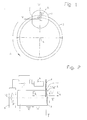
- a single crystal 1 of substantially cylindrical shape with a central longitudinal axis M is from a holder, not shown held.
- An inner hole cutting disc 2 which in known Way of a metal disk with a concentric hole at the boundary by applying diamond grains a cutting edge 3 is formed, is about an axis of rotation R rotatably supported relative to the single crystal, that the center longitudinal axis M of the single crystal and the axis of rotation R of the cutting disc parallel to each other.
- It is an unillustrated drive provided with the blade 2 at a defined speed about the rotation axis R in the direction shown in Fig. 1 A is rotatable.
- the single crystal 1 is via a drive a feed unit in the feed direction shown in Fig. 2 V in the direction of the cutting disc 2 so movable, that the cutting disc 2, the single crystal 1 completely in a plane perpendicular to its central longitudinal axis M cut through can. Furthermore, a drive is provided for moving of the single crystal 1 perpendicular to the cutting disk 2 or along the direction of its central longitudinal axis at a speed w.
- the single crystal is 1 not completely cylindrical, but has a flat Outside surface section 4, the so-called flat, the so after culturing the single crystal 1 in a defined manner has been that an angle ⁇ , a certain crystallographic direction K, for GaAs, for example, one [011] direction, with the normal N on the flat outer surface portion 4, in a plane perpendicular to the central longitudinal axis M is known.
- the angle ⁇ is known is, therefore, is also an angle ⁇ between the particular crystallographic Direction K and the feed direction V of Single crystal in a plane perpendicular to the center longitudinal axis M of the single crystal and thus in the parting plane T known.
- a notch was named instead of the flats Incision provided on the outside of the single crystal can be. Decisive is only an external feature, its arrangement to the particular crystallographic direction is known.
- the apparatus further instructs the end of the single crystal 1 facing away from the cutting disk 2 a device 5 for rotating the single crystal 1 around its Center longitudinal axis M on. Furthermore, a sensor 6 is provided for measuring a deflection X of the cutting disk 2 from the Parting plane T out when separating a disc-shaped portion 1a of the single crystal 1, the later wafer forms.
- the sensor 6 and the device 5 for rotating the Monocrystal 1 are connected via a control device 7 with each other connected, which is designed such that in dependence from the measured deflection X of the cutting wheel 2, the rotating device 5 is actuated, so that the single crystal 1 in a predetermined azimuthal position is rotated so that the specific crystallographic direction K with the feed direction V one of the measured deflection X of the cutting disc. 2 corresponding predefined angle ⁇ occupies.
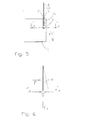
- the device For separating a single crystal a wire sawing device, such as is shown in Figures 3 and 4.
- the in Figures 1 and 2 shown device corresponding parts are with the provided the same reference numerals.
- the wire saw 8 consists of a variety of parallel wires 8a, 8b, 8c, not shown above Rollers are stretched and in planes perpendicular to Center longitudinal axis M of the single crystal 1 in the direction shown by arrows Directions A and B are movable.
- the device comprises a device 9 for applying a paste, which contains diamond grains, on the wires 8a, 8b, 8c a side of the single crystal 1 and a device 10 for Cleaning the wires after passing through the monocrystal and for discharging the Abtragages when passing the wires through the single crystal.
- a device 10 for Cleaning the wires after passing through the monocrystal and for discharging the Abtragages when passing the wires through the single crystal.
- the diamond grain is already solid embedded in the wire and applying by means of a Paste is not required.
- Analogous to that shown in Fig. 2 Device has this embodiment, as shown in FIG. 4, also means 5 for turning of the single crystal 1 and a sensor, the deflection of a Wire 8a, 8b and 8c detected, and a control device 7th for controlling the device 5 for rotating the single crystal 1 depending on the detected wire deflection.
- the holder After the assembly of the single crystal 1 in the holder, the holder is advanced in the direction W shown in Fig. 2 via the drive so that between the free end 1a of the single crystal and the cutting disc 2 remains a distance a, which is slightly more than the thickness of a wafer to be produced. Then, the single crystal 1 is moved via the drive in the feed direction V shown in FIGS. 2 and 5 at a feed rate v against the cutting disk 2, which in turn rotates about its axis of rotation in the direction A shown in FIG. The rotating cutting disk 2 engages the single crystal 1 for separating a portion 1a, which forms the later wafer, from the single crystal 1.
- the diamond grains of the cutting edge 3 of the cutting disk 2 generate microcracks in the separation process after reaching a critical penetration depth into the single crystal 1, which lead through cross-linking to material removal.
- This critical penetration depends on the direction of movement of the grain to the particular crystallographic direction K.
- the critical depth of penetration depends on the angle p, which includes the particular crystallographic direction K with the feed direction V in a plane perpendicular to the central longitudinal axis M of the single crystal. It has been found that the critical penetration depth on respective opposite sides S, S 'of the engaging blade 2 is different.
- FIG. 7 shows the critical penetration depth on the front side S opposite the cutting disk 2 and the rear side S 'for different angular settings p of the determined crystallographic direction K relative to the feed direction V.
- the resultant force F resulting from the sum of the constraining forces F x - , F x + and Fz is dependent on the feed direction V relative to the determined crystallographic direction K, ie the angle ⁇ include these two directions with each other in the parting plane perpendicular to the central longitudinal axis of the single crystal 1.
- the angle ⁇ include these two directions with each other in the parting plane perpendicular to the central longitudinal axis of the single crystal 1.
- the aforementioned constraining forces are used to correct the transverse deflection X of the cutting wheel during the cut.
- the deflection X of the cutting disk or the axial cutting force component F a or F b is measured by means of the sensor 6.
- the device 5 for rotating the monocrystal 1 is actuated via the control device 7 such that the angle p between the determined crystallographic direction K and the feed direction V is set so that the transverse deflection by means of the constraining forces F x - , F x + is controlled at substantially zero.
- the method is for the wire cutting apparatus shown in Figs. 3 and 4 equally applicable, in which case then the Deflection of one or more wires is measured.
- the preferred angles of particular crystallographic Direction K to the feed direction V, where the deflection of the cutting tool to cut to zero, are of the Material of the single crystal dependent. These angles are for each material of a single crystal empirically by means of a Test method determined.
- Fig. 11 is a single crystal 20 of a particular material in a plurality of discs 20a to 20e separated, the thickness thereof a plurality of thicknesses of the wafers to be produced later equivalent.
- the discs are then placed on a holder 21 glued so that their flat outer surface portions (Flats) 40a to 40e e.g. in a wire saw device in each case different angles to the feed direction V are arranged.
- the procedure is repeated until the preferred angles have been determined for optimal cutting are.
- the angles thus determined serve as a starting point for the Separation process later to be separated single crystals in the in the Fig. 1 to 4 shown devices, wherein the readjustment the adjustment of the angle on the device 5 and the Control device 7 for correction during the separation process serve.
- the apparatus shown in FIG. 12 is the adjusting device shown in FIG intended.
- the adjusting device has a base plate 50 and a vertically from this upwardly extending support 51 on.
- a Tab 52 provided, for example, on a non-illustrated Rail can be moved up and down in the vertical direction is and by means of a fastening device 53 in a predetermined height can be locked.
- the rider 52 points a projection 54 in the form of an angle, the lower edge 54a with the vertical includes a predetermined angle ⁇ .
- the single crystal 1 By pushing the single crystal 1 together the connector 55 and the bar 56 at the angle 54, the single crystal 1 is adjusted so that its level Outer surface portion 4 at the lower edge 54a of the angular Approach 54 is applied.
- the angle ⁇ , the lower edge 54a of the neck 54 forms with the vertical, is doing so chosen that for this specific single crystal 1 a certain preferred angle p between the particular crystallographic Set direction K to the vertical becomes.
- the feed direction V corresponds to the vertical, so that the angle ⁇ is defined.
- the invention described above has the particular advantage on that in particular GaAs wafer with a diameter of 6 inches or possibly even more easily with the inner hole saws can be disconnected because of an increased feed rate is possible.
- the invention is not for the separation of semiconductor single crystals (pure elements, semiconductors, semiconducting compounds) limited.
- inventive method and the Rather, devices can also be used to separate any single crystals, used as optical single crystals or ceramics become.
Landscapes
- Engineering & Computer Science (AREA)
- Mechanical Engineering (AREA)
- Chemical & Material Sciences (AREA)
- Crystallography & Structural Chemistry (AREA)
- Materials Engineering (AREA)
- Metallurgy (AREA)
- Organic Chemistry (AREA)
- Processing Of Stones Or Stones Resemblance Materials (AREA)
- Crystals, And After-Treatments Of Crystals (AREA)
- Mechanical Treatment Of Semiconductor (AREA)
- Analysing Materials By The Use Of Radiation (AREA)
Applications Claiming Priority (3)
| Application Number | Priority Date | Filing Date | Title |
|---|---|---|---|
| DE10052154 | 2000-10-20 | ||
| DE10052154A DE10052154A1 (de) | 2000-10-20 | 2000-10-20 | Verfahren und Vorrichtung zum Trennen von Einkristallen, Justiervorrichtung und Testverfahren zum Ermitteln einer Orientierung eines Einkristalls für ein derartiges Verfahren |
| PCT/EP2001/008800 WO2002034973A1 (de) | 2000-10-20 | 2001-07-30 | Verfahren und vorrichtung zum trennen von einkristallen, sowie eine justiervorrichtung und ein testverfahren zum ermitteln einer kristallorientierung |
Publications (2)
| Publication Number | Publication Date |
|---|---|
| EP1332247A1 EP1332247A1 (de) | 2003-08-06 |
| EP1332247B1 true EP1332247B1 (de) | 2004-09-29 |
Family
ID=7660519
Family Applications (1)
| Application Number | Title | Priority Date | Filing Date |
|---|---|---|---|
| EP01960587A Expired - Lifetime EP1332247B1 (de) | 2000-10-20 | 2001-07-30 | Verfahren und vorrichtung zum trennen von einkristallen, sowie eine justiervorrichtung und ein testverfahren zum ermitteln einer kristallorientierung |
Country Status (11)
| Country | Link |
|---|---|
| US (1) | US7137865B2 (cs) |
| EP (1) | EP1332247B1 (cs) |
| JP (1) | JP5087202B2 (cs) |
| CN (1) | CN1270000C (cs) |
| AT (1) | ATE278052T1 (cs) |
| CZ (1) | CZ297783B6 (cs) |
| DE (2) | DE10052154A1 (cs) |
| RU (1) | RU2251598C2 (cs) |
| SK (1) | SK286535B6 (cs) |
| TW (1) | TW521340B (cs) |
| WO (1) | WO2002034973A1 (cs) |
Families Citing this family (24)
| Publication number | Priority date | Publication date | Assignee | Title |
|---|---|---|---|---|
| DE10128630A1 (de) | 2001-06-13 | 2003-01-02 | Freiberger Compound Mat Gmbh | Vorrichtung und Verfahren zur Bestimmung der Orientierung einer kristallografischen Ebene relativ zu einer Kristalloberfläche sowie Vorrichtung und Verfahren zum Trennen eines Einkristalls in einer Trennmaschine |
| JP4525353B2 (ja) * | 2005-01-07 | 2010-08-18 | 住友電気工業株式会社 | Iii族窒化物基板の製造方法 |
| DE102005040343A1 (de) | 2005-08-25 | 2007-03-01 | Freiberger Compound Materials Gmbh | Verfahren, Vorrichtung und Slurry zum Drahtsägen |
| EP2275241B1 (de) | 2005-08-25 | 2012-10-17 | Freiberger Compound Materials GmbH | Drahtsäge und Verfahren zum Trennen eines Werkstücks mittels Drahtsägen |
| CA2690791C (en) * | 2007-06-25 | 2012-10-30 | Saint-Gobain Ceramics & Plastics, Inc. | Methods of crystallographically reorienting single crystal bodies |
| KR20100094484A (ko) * | 2007-12-19 | 2010-08-26 | 아사히 가라스 가부시키가이샤 | 에테르 조성물 |
| JP5475772B2 (ja) * | 2008-07-11 | 2014-04-16 | サンーゴバン アブレイシブズ,インコーポレイティド | ワイヤスライシングシステム |
| CN101486231B (zh) * | 2009-01-22 | 2011-12-07 | 四川大学 | 黄铜矿类负单轴晶体制备红外非线性光学元件的定向切割方法 |
| RU2411606C1 (ru) * | 2009-06-08 | 2011-02-10 | Учреждение российской академии наук Институт кристаллографии имени А.В. Шубникова РАН | Способ доводки ориентации пластин полупроводниковых и оптических материалов |
| DE102010018570B4 (de) * | 2010-04-28 | 2017-06-08 | Siltronic Ag | Verfahren zur Herstellung einer Vielzahl von Halbleiterscheiben durch Bearbeiten eines Einkristalls |
| US8259901B1 (en) | 2010-05-25 | 2012-09-04 | Rubicon Technology, Inc. | Intelligent machines and process for production of monocrystalline products with goniometer continual feedback |
| JP2012045682A (ja) * | 2010-08-27 | 2012-03-08 | Tokuriki Honten Co Ltd | 固定砥粒ワイヤーソー装置 |
| CN102152410A (zh) * | 2010-12-23 | 2011-08-17 | 万向硅峰电子股份有限公司 | 一种旋转单晶棒调整晶向偏移的切割方法 |
| WO2012165108A1 (ja) * | 2011-06-02 | 2012-12-06 | 住友電気工業株式会社 | 炭化珪素基板の製造方法 |
| US10052848B2 (en) | 2012-03-06 | 2018-08-21 | Apple Inc. | Sapphire laminates |
| US9154678B2 (en) | 2013-12-11 | 2015-10-06 | Apple Inc. | Cover glass arrangement for an electronic device |
| JP6000235B2 (ja) * | 2013-12-24 | 2016-09-28 | 信越半導体株式会社 | ワークの切断方法及びワーク保持治具 |
| US10406634B2 (en) | 2015-07-01 | 2019-09-10 | Apple Inc. | Enhancing strength in laser cutting of ceramic components |
| JP6613482B2 (ja) * | 2015-09-03 | 2019-12-04 | 日本電波工業株式会社 | 水晶振動子 |
| CN111638305B (zh) * | 2020-06-08 | 2023-09-22 | 郑州磨料磨具磨削研究所有限公司 | 一种用于确定单晶材料最优加工方向的方法 |
| DE102020209092A1 (de) * | 2020-07-21 | 2022-01-27 | Sicrystal Gmbh | Kristallstrukturorientierung in Halbleiter-Halbzeugen und Halbleitersubstraten zum Verringern von Sprüngen und Verfahren zum Einstellen von dieser |
| CN112590032B (zh) * | 2020-12-03 | 2022-12-02 | 天津市环智新能源技术有限公司 | 一种太阳能硅片及其粗糙度控制方法 |
| CN114161588B (zh) * | 2021-12-09 | 2024-08-06 | 浙江翔日科技炭素有限公司 | 石墨热场柱状料旋切内掏的装置及方法 |
| CN115692229A (zh) * | 2022-10-31 | 2023-02-03 | 东莞忆联信息系统有限公司 | 一种刀片位置偏移检测结构及其检测方法、切割装置 |
Family Cites Families (21)
| Publication number | Priority date | Publication date | Assignee | Title |
|---|---|---|---|---|
| GB628508A (en) | 1947-05-06 | 1949-08-30 | Standard Telephones Cables Ltd | Improvements in or relating to machines for cutting crystalline material |
| JPS56129114A (en) * | 1980-03-17 | 1981-10-09 | Tokyo Shibaura Electric Co | Method of cutting monocrystal |
| JPH0761647B2 (ja) * | 1985-06-11 | 1995-07-05 | 日立電線株式会社 | 半導体結晶インゴットのスライス方法 |
| DE3640645A1 (de) * | 1986-11-28 | 1988-06-09 | Wacker Chemitronic | Verfahren zum zersaegen von kristallstaeben oder -bloecken vermittels innenlochsaege in duenne scheiben |
| JPH0635107B2 (ja) * | 1987-12-26 | 1994-05-11 | 株式会社タカトリハイテック | ワイヤソー |
| JP2655677B2 (ja) * | 1988-04-26 | 1997-09-24 | トーヨーエイテック株式会社 | スライシングマシン |
| DE3826698A1 (de) * | 1988-08-05 | 1990-02-08 | Wacker Chemitronic | Verfahren und vorrichtung zur kontrolle des schnittverlaufes beim abtrennen von scheiben von nichtmagnetisierbaren werkstuecken |
| US5131975A (en) * | 1990-07-10 | 1992-07-21 | The Regents Of The University Of California | Controlled growth of semiconductor crystals |
| CH690845A5 (de) * | 1994-05-19 | 2001-02-15 | Tokyo Seimitsu Co Ltd | Verfahren zum Positionieren eines Werkstücks und Vorrichtung hierfür. |
| CH690422A5 (fr) | 1995-04-22 | 2000-09-15 | Hct Shaping Systems Sa | Dispositif pour l'orientation de monocristaux en vue d'une découpe dans un plan prédéterminé et selon une direction qui minimise la longueur de coupe. |
| EP0738572B1 (fr) * | 1995-04-22 | 2004-01-21 | HCT Shaping Systems SA | Procédé pour l'orientation de monocristaux pour le découpage dans une machine de découpage et dispositif pour la mise en oeuvre de ce procédé |
| JP2842307B2 (ja) * | 1995-06-30 | 1999-01-06 | 住友電気工業株式会社 | Iii−v族化合物半導体結晶の切断方法 |
| JPH0985736A (ja) * | 1995-09-22 | 1997-03-31 | Toray Eng Co Ltd | ワイヤ式切断装置 |
| CH691045A5 (fr) * | 1996-04-16 | 2001-04-12 | Hct Shaping Systems Sa | Procédé pour l'orientation de plusieurs pièces cristallines posées côte à côte sur un support de découpage en vue d'une découpe simultanée dans une machine de découpage et dispositif pour la |
| CH690907A5 (fr) * | 1996-05-23 | 2001-02-28 | Hct Shaping Systems Sa | Dispositif de sciage par fil |
| CH692331A5 (de) * | 1996-06-04 | 2002-05-15 | Tokyo Seimitsu Co Ltd | Drahtsäge und Schneidverfahren unter Einsatz derselben. |
| JPH1110510A (ja) * | 1997-06-19 | 1999-01-19 | Nippei Toyama Corp | ワイヤソー装置及びワーク切削方法 |
| US5878737A (en) * | 1997-07-07 | 1999-03-09 | Laser Technology West Limited | Apparatus and method for slicing a workpiece utilizing a diamond impregnated wire |
| JP3205718B2 (ja) | 1997-08-29 | 2001-09-04 | 株式会社スーパーシリコン研究所 | ワイヤソー切断方法及び装置 |
| JPH11235718A (ja) * | 1998-02-20 | 1999-08-31 | Hitachi Cable Ltd | 半導体インゴットの切断方法 |
| DE19825051A1 (de) * | 1998-06-04 | 1999-12-09 | Wacker Siltronic Halbleitermat | Verfahren und Vorrichtung zur Herstellung eines zylinderförmigen Einkristalls und Verfahren zum Abtrennen von Halbleiterscheiben |
-
2000
- 2000-10-20 DE DE10052154A patent/DE10052154A1/de not_active Ceased
-
2001
- 2001-07-30 WO PCT/EP2001/008800 patent/WO2002034973A1/de not_active Ceased
- 2001-07-30 JP JP2002537937A patent/JP5087202B2/ja not_active Expired - Lifetime
- 2001-07-30 CZ CZ20031102A patent/CZ297783B6/cs not_active IP Right Cessation
- 2001-07-30 US US10/399,672 patent/US7137865B2/en not_active Expired - Lifetime
- 2001-07-30 AT AT01960587T patent/ATE278052T1/de not_active IP Right Cessation
- 2001-07-30 SK SK450-2003A patent/SK286535B6/sk not_active IP Right Cessation
- 2001-07-30 RU RU2003114430/15A patent/RU2251598C2/ru active
- 2001-07-30 CN CNB018176313A patent/CN1270000C/zh not_active Expired - Lifetime
- 2001-07-30 DE DE50103912T patent/DE50103912D1/de not_active Expired - Lifetime
- 2001-07-30 EP EP01960587A patent/EP1332247B1/de not_active Expired - Lifetime
- 2001-10-04 TW TW090124464A patent/TW521340B/zh not_active IP Right Cessation
Also Published As
| Publication number | Publication date |
|---|---|
| ATE278052T1 (de) | 2004-10-15 |
| US20040118338A1 (en) | 2004-06-24 |
| RU2251598C2 (ru) | 2005-05-10 |
| CZ297783B6 (cs) | 2007-03-28 |
| US7137865B2 (en) | 2006-11-21 |
| SK286535B6 (sk) | 2008-12-05 |
| JP5087202B2 (ja) | 2012-12-05 |
| CN1270000C (zh) | 2006-08-16 |
| JP2004512251A (ja) | 2004-04-22 |
| CN1469942A (zh) | 2004-01-21 |
| TW521340B (en) | 2003-02-21 |
| WO2002034973A1 (de) | 2002-05-02 |
| DE50103912D1 (de) | 2004-11-04 |
| DE10052154A1 (de) | 2002-05-08 |
| SK4502003A3 (en) | 2003-11-04 |
| EP1332247A1 (de) | 2003-08-06 |
| CZ20031102A3 (cs) | 2003-09-17 |
Similar Documents
| Publication | Publication Date | Title |
|---|---|---|
| EP1332247B1 (de) | Verfahren und vorrichtung zum trennen von einkristallen, sowie eine justiervorrichtung und ein testverfahren zum ermitteln einer kristallorientierung | |
| DE69734414T2 (de) | Verfahren zum Zerschneiden eines Einkristallbarren aus Halbleitermaterial | |
| DE102008051673B4 (de) | Verfahren zum gleichzeitigen Auftrennen eines Verbundstabs aus Silicium in eine Vielzahl von Scheiben | |
| DE2819420C2 (de) | Verfahren zum Vorbereiten eines Einkristall-Rohlings, der mittels einer Innenlochsäge in Scheiben zersägt wird | |
| EP1568457A1 (de) | Vorrichtung und Verfahren zur Bestimmung der Orientierung einer kristallografischen Ebene relativ zu einer Kristalloberfläche | |
| DE2355339C3 (de) | Präzisionshaltevorrichtung für zylindrische Werkstücke | |
| DE3906091A1 (de) | Verfahren zum zersaegen von stabfoermigen werkstuecken in scheiben mittels innenlochsaege, sowie innenlochsaegen zu seiner durchfuehrung | |
| DE3613132A1 (de) | Verfahren zum zerteilen von harten, nichtmetallischen werkstoffen | |
| DE19825051A1 (de) | Verfahren und Vorrichtung zur Herstellung eines zylinderförmigen Einkristalls und Verfahren zum Abtrennen von Halbleiterscheiben | |
| DE2061135A1 (de) | Praezisionssaegevorrichtung | |
| DE102005047114A1 (de) | Schleifprozess und Vorrichtung mit Anordnung zum Schleifen mit konstanter Schleiflast | |
| DE102007028439A1 (de) | Verfahren zum Abtrennen einer Mehrzahl von Halbleiterscheiben von einem Halbleitermaterial-Rohblock | |
| DE102010007459B4 (de) | Verfahren zum Abtrennen einer Vielzahl von Scheiben von einem Kristall aus Halbleitermaterial | |
| EP0432637B1 (de) | Vorrichtung zum Nachschärfen der Schneidkante von Trennwerkzeugen beim Abtrennen von Scheiben von stab- oder blockförmigen Werkstücken, insbesondere aus Halbleitermaterial, ihre Verwendung und Sägeverfahren | |
| DE19526711A1 (de) | Verfahren zur Bearbeitung von Siliciumwafern | |
| EP0464668B1 (de) | Spannsystem für ein Innenlochsägeblatt und seine Verwendung beim Zersägen von Stäben, insbesondere aus Halbleitermaterial, in Scheiben | |
| DE212017000282U1 (de) | Fräser mit Kassette und einer verbesserten Kassettenbefestigungseinrichtung hierfür | |
| EP0204958B1 (de) | Vorrichtung zum Schleifen und Läppen von Dichtflächen in Schiebern und dergleichen in situ oder in der Werkstatt | |
| DE19825050C2 (de) | Verfahren zum Anordnen und Orientieren von Einkristallen zum Abtrennen von Scheiben auf einer ein Drahtgatter aufweisenden Drahtsäge | |
| EP0791444B1 (de) | Verfahren zur Herstellung von Halbleiterscheiben | |
| DE68924502T2 (de) | Verfahren zur Herstellung von Einzelsubstraten. | |
| EP3492218B1 (de) | Werkstückträgervorrichtung | |
| DE4321048C2 (de) | Halterungsvorrichtung sowie Verfahren zur Herstellung von Glasleisten | |
| DE102013202028A1 (de) | Verfahren zum Herstellen von Wafern, insbesondere von Wafern für Solarzellen, und Vorrichtung zum Herstellen von Wafern | |
| DE102012220952A1 (de) | Verfahren zur mechanischen Bearbeitung der Kante einer Halbleiterscheibe |
Legal Events
| Date | Code | Title | Description |
|---|---|---|---|
| PUAI | Public reference made under article 153(3) epc to a published international application that has entered the european phase |
Free format text: ORIGINAL CODE: 0009012 |
|
| 17P | Request for examination filed |
Effective date: 20030307 |
|
| AK | Designated contracting states |
Designated state(s): AT BE CH CY DE DK ES FI FR GB GR IE IT LI LU MC NL PT SE TR |
|
| GRAP | Despatch of communication of intention to grant a patent |
Free format text: ORIGINAL CODE: EPIDOSNIGR1 |
|
| GRAS | Grant fee paid |
Free format text: ORIGINAL CODE: EPIDOSNIGR3 |
|
| GRAA | (expected) grant |
Free format text: ORIGINAL CODE: 0009210 |
|
| AK | Designated contracting states |
Kind code of ref document: B1 Designated state(s): AT BE CH CY DE DK ES FI FR GB GR IE IT LI LU MC NL PT SE TR |
|
| PG25 | Lapsed in a contracting state [announced via postgrant information from national office to epo] |
Ref country code: TR Free format text: LAPSE BECAUSE OF FAILURE TO SUBMIT A TRANSLATION OF THE DESCRIPTION OR TO PAY THE FEE WITHIN THE PRESCRIBED TIME-LIMIT Effective date: 20040929 Ref country code: NL Free format text: LAPSE BECAUSE OF FAILURE TO SUBMIT A TRANSLATION OF THE DESCRIPTION OR TO PAY THE FEE WITHIN THE PRESCRIBED TIME-LIMIT Effective date: 20040929 Ref country code: IE Free format text: LAPSE BECAUSE OF FAILURE TO SUBMIT A TRANSLATION OF THE DESCRIPTION OR TO PAY THE FEE WITHIN THE PRESCRIBED TIME-LIMIT Effective date: 20040929 Ref country code: FI Free format text: LAPSE BECAUSE OF FAILURE TO SUBMIT A TRANSLATION OF THE DESCRIPTION OR TO PAY THE FEE WITHIN THE PRESCRIBED TIME-LIMIT Effective date: 20040929 |
|
| REG | Reference to a national code |
Ref country code: GB Ref legal event code: FG4D Free format text: NOT ENGLISH |
|
| REG | Reference to a national code |
Ref country code: CH Ref legal event code: EP |
|
| REG | Reference to a national code |
Ref country code: CH Ref legal event code: NV Representative=s name: NOVAGRAAF INTERNATIONAL SA |
|
| GBT | Gb: translation of ep patent filed (gb section 77(6)(a)/1977) | ||
| REG | Reference to a national code |
Ref country code: IE Ref legal event code: FG4D Free format text: GERMAN |
|
| REF | Corresponds to: |
Ref document number: 50103912 Country of ref document: DE Date of ref document: 20041104 Kind code of ref document: P |
|
| PG25 | Lapsed in a contracting state [announced via postgrant information from national office to epo] |
Ref country code: SE Free format text: LAPSE BECAUSE OF FAILURE TO SUBMIT A TRANSLATION OF THE DESCRIPTION OR TO PAY THE FEE WITHIN THE PRESCRIBED TIME-LIMIT Effective date: 20041229 Ref country code: GR Free format text: LAPSE BECAUSE OF FAILURE TO SUBMIT A TRANSLATION OF THE DESCRIPTION OR TO PAY THE FEE WITHIN THE PRESCRIBED TIME-LIMIT Effective date: 20041229 Ref country code: DK Free format text: LAPSE BECAUSE OF FAILURE TO SUBMIT A TRANSLATION OF THE DESCRIPTION OR TO PAY THE FEE WITHIN THE PRESCRIBED TIME-LIMIT Effective date: 20041229 |
|
| PG25 | Lapsed in a contracting state [announced via postgrant information from national office to epo] |
Ref country code: ES Free format text: LAPSE BECAUSE OF FAILURE TO SUBMIT A TRANSLATION OF THE DESCRIPTION OR TO PAY THE FEE WITHIN THE PRESCRIBED TIME-LIMIT Effective date: 20050109 |
|
| NLV1 | Nl: lapsed or annulled due to failure to fulfill the requirements of art. 29p and 29m of the patents act | ||
| REG | Reference to a national code |
Ref country code: IE Ref legal event code: FD4D |
|
| ET | Fr: translation filed | ||
| PGFP | Annual fee paid to national office [announced via postgrant information from national office to epo] |
Ref country code: AT Payment date: 20050628 Year of fee payment: 5 |
|
| PG25 | Lapsed in a contracting state [announced via postgrant information from national office to epo] |
Ref country code: LU Free format text: LAPSE BECAUSE OF NON-PAYMENT OF DUE FEES Effective date: 20050730 Ref country code: CY Free format text: LAPSE BECAUSE OF FAILURE TO SUBMIT A TRANSLATION OF THE DESCRIPTION OR TO PAY THE FEE WITHIN THE PRESCRIBED TIME-LIMIT Effective date: 20050730 |
|
| PG25 | Lapsed in a contracting state [announced via postgrant information from national office to epo] |
Ref country code: MC Free format text: LAPSE BECAUSE OF NON-PAYMENT OF DUE FEES Effective date: 20050731 |
|
| PLBE | No opposition filed within time limit |
Free format text: ORIGINAL CODE: 0009261 |
|
| STAA | Information on the status of an ep patent application or granted ep patent |
Free format text: STATUS: NO OPPOSITION FILED WITHIN TIME LIMIT |
|
| 26N | No opposition filed |
Effective date: 20050630 |
|
| PG25 | Lapsed in a contracting state [announced via postgrant information from national office to epo] |
Ref country code: AT Free format text: LAPSE BECAUSE OF NON-PAYMENT OF DUE FEES Effective date: 20060730 |
|
| PG25 | Lapsed in a contracting state [announced via postgrant information from national office to epo] |
Ref country code: PT Free format text: LAPSE BECAUSE OF NON-PAYMENT OF DUE FEES Effective date: 20050228 |
|
| REG | Reference to a national code |
Ref country code: CH Ref legal event code: PFA Owner name: FREIBERGER COMPOUND MATERIALS GMBH Free format text: FREIBERGER COMPOUND MATERIALS GMBH#AM JUNGER LOEWE SCHACHT 5#09599 FREIBERG (DE) -TRANSFER TO- FREIBERGER COMPOUND MATERIALS GMBH#AM JUNGER LOEWE SCHACHT 5#09599 FREIBERG (DE) |
|
| REG | Reference to a national code |
Ref country code: FR Ref legal event code: PLFP Year of fee payment: 16 |
|
| REG | Reference to a national code |
Ref country code: FR Ref legal event code: PLFP Year of fee payment: 17 |
|
| REG | Reference to a national code |
Ref country code: FR Ref legal event code: PLFP Year of fee payment: 18 |
|
| PGFP | Annual fee paid to national office [announced via postgrant information from national office to epo] |
Ref country code: DE Payment date: 20200729 Year of fee payment: 20 Ref country code: FR Payment date: 20200727 Year of fee payment: 20 Ref country code: GB Payment date: 20200724 Year of fee payment: 20 |
|
| PGFP | Annual fee paid to national office [announced via postgrant information from national office to epo] |
Ref country code: BE Payment date: 20200722 Year of fee payment: 20 Ref country code: CH Payment date: 20200724 Year of fee payment: 20 Ref country code: IT Payment date: 20200731 Year of fee payment: 20 |
|
| REG | Reference to a national code |
Ref country code: DE Ref legal event code: R071 Ref document number: 50103912 Country of ref document: DE |
|
| REG | Reference to a national code |
Ref country code: CH Ref legal event code: PL |
|
| REG | Reference to a national code |
Ref country code: BE Ref legal event code: MK Effective date: 20210730 Ref country code: GB Ref legal event code: PE20 Expiry date: 20210729 |
|
| PG25 | Lapsed in a contracting state [announced via postgrant information from national office to epo] |
Ref country code: GB Free format text: LAPSE BECAUSE OF EXPIRATION OF PROTECTION Effective date: 20210729 |