EP1333008B1 - Vorrichtung und Verfahren zur thermischen Isolierung von Siliciumstrukturen - Google Patents
Vorrichtung und Verfahren zur thermischen Isolierung von Siliciumstrukturen Download PDFInfo
- Publication number
- EP1333008B1 EP1333008B1 EP03250016A EP03250016A EP1333008B1 EP 1333008 B1 EP1333008 B1 EP 1333008B1 EP 03250016 A EP03250016 A EP 03250016A EP 03250016 A EP03250016 A EP 03250016A EP 1333008 B1 EP1333008 B1 EP 1333008B1
- Authority
- EP
- European Patent Office
- Prior art keywords
- silicon
- substrate
- layer
- forming
- insulation layer
- Prior art date
- Legal status (The legal status is an assumption and is not a legal conclusion. Google has not performed a legal analysis and makes no representation as to the accuracy of the status listed.)
- Expired - Lifetime
Links
Images




Classifications
-
- B—PERFORMING OPERATIONS; TRANSPORTING
- B81—MICROSTRUCTURAL TECHNOLOGY
- B81B—MICROSTRUCTURAL DEVICES OR SYSTEMS, e.g. MICROMECHANICAL DEVICES
- B81B3/00—Devices comprising flexible or deformable elements, e.g. comprising elastic tongues or membranes
- B81B3/0064—Constitution or structural means for improving or controlling the physical properties of a device
- B81B3/0081—Thermal properties
-
- B—PERFORMING OPERATIONS; TRANSPORTING
- B81—MICROSTRUCTURAL TECHNOLOGY
- B81C—PROCESSES OR APPARATUS SPECIALLY ADAPTED FOR THE MANUFACTURE OR TREATMENT OF MICROSTRUCTURAL DEVICES OR SYSTEMS
- B81C1/00—Manufacture or treatment of devices or systems in or on a substrate
- B81C1/00436—Shaping materials, i.e. techniques for structuring the substrate or the layers on the substrate
- B81C1/00555—Achieving a desired geometry, i.e. controlling etch rates, anisotropy or selectivity
- B81C1/00595—Control etch selectivity
-
- G—PHYSICS
- G02—OPTICS
- G02F—OPTICAL DEVICES OR ARRANGEMENTS FOR THE CONTROL OF LIGHT BY MODIFICATION OF THE OPTICAL PROPERTIES OF THE MEDIA OF THE ELEMENTS INVOLVED THEREIN; NON-LINEAR OPTICS; FREQUENCY-CHANGING OF LIGHT; OPTICAL LOGIC ELEMENTS; OPTICAL ANALOGUE/DIGITAL CONVERTERS
- G02F1/00—Devices or arrangements for the control of the intensity, colour, phase, polarisation or direction of light arriving from an independent light source, e.g. switching, gating or modulating; Non-linear optics
- G02F1/01—Devices or arrangements for the control of the intensity, colour, phase, polarisation or direction of light arriving from an independent light source, e.g. switching, gating or modulating; Non-linear optics for the control of the intensity, phase, polarisation or colour
- G02F1/015—Devices or arrangements for the control of the intensity, colour, phase, polarisation or direction of light arriving from an independent light source, e.g. switching, gating or modulating; Non-linear optics for the control of the intensity, phase, polarisation or colour based on semiconductor elements having potential barriers, e.g. having a PN or PIN junction
- G02F1/025—Devices or arrangements for the control of the intensity, colour, phase, polarisation or direction of light arriving from an independent light source, e.g. switching, gating or modulating; Non-linear optics for the control of the intensity, phase, polarisation or colour based on semiconductor elements having potential barriers, e.g. having a PN or PIN junction in an optical waveguide structure
-
- H—ELECTRICITY
- H10—SEMICONDUCTOR DEVICES; ELECTRIC SOLID-STATE DEVICES NOT OTHERWISE PROVIDED FOR
- H10W—GENERIC PACKAGES, INTERCONNECTIONS, CONNECTORS OR OTHER CONSTRUCTIONAL DETAILS OF DEVICES COVERED BY CLASS H10
- H10W10/00—Isolation regions in semiconductor bodies between components of integrated devices
- H10W10/01—Manufacture or treatment
- H10W10/021—Manufacture or treatment of air gaps
-
- H—ELECTRICITY
- H10—SEMICONDUCTOR DEVICES; ELECTRIC SOLID-STATE DEVICES NOT OTHERWISE PROVIDED FOR
- H10W—GENERIC PACKAGES, INTERCONNECTIONS, CONNECTORS OR OTHER CONSTRUCTIONAL DETAILS OF DEVICES COVERED BY CLASS H10
- H10W10/00—Isolation regions in semiconductor bodies between components of integrated devices
- H10W10/20—Air gaps
-
- B—PERFORMING OPERATIONS; TRANSPORTING
- B81—MICROSTRUCTURAL TECHNOLOGY
- B81B—MICROSTRUCTURAL DEVICES OR SYSTEMS, e.g. MICROMECHANICAL DEVICES
- B81B2203/00—Basic microelectromechanical structures
- B81B2203/01—Suspended structures, i.e. structures allowing a movement
- B81B2203/0109—Bridges
-
- G—PHYSICS
- G02—OPTICS
- G02F—OPTICAL DEVICES OR ARRANGEMENTS FOR THE CONTROL OF LIGHT BY MODIFICATION OF THE OPTICAL PROPERTIES OF THE MEDIA OF THE ELEMENTS INVOLVED THEREIN; NON-LINEAR OPTICS; FREQUENCY-CHANGING OF LIGHT; OPTICAL LOGIC ELEMENTS; OPTICAL ANALOGUE/DIGITAL CONVERTERS
- G02F1/00—Devices or arrangements for the control of the intensity, colour, phase, polarisation or direction of light arriving from an independent light source, e.g. switching, gating or modulating; Non-linear optics
- G02F1/01—Devices or arrangements for the control of the intensity, colour, phase, polarisation or direction of light arriving from an independent light source, e.g. switching, gating or modulating; Non-linear optics for the control of the intensity, phase, polarisation or colour
- G02F1/0147—Devices or arrangements for the control of the intensity, colour, phase, polarisation or direction of light arriving from an independent light source, e.g. switching, gating or modulating; Non-linear optics for the control of the intensity, phase, polarisation or colour based on thermo-optic effects
Definitions
- This invention relates to systems and methods for thermal isolation of a silicon structure.
- the systems and methods of this invention relate to micromachined or microelectromechanical system based devices and the fabrication thereof.
- the device comprises a silicon on insulator (SOI) wafer including a layer of silicon 4 separated from a silicon substrate 5 by an insulator layer 6 formed of silicon dioxide. A portion of the layer of silicon 4 comprises a waveguide 1 that extends across a V-groove 2 formed in the silicon substrate 5. In that manner, the waveguide 1 is substantially thermally isolated from the silicon substrate 5.
- SOI silicon on insulator
- the waveguide 1 is a rib waveguide.
- An oxide coating 6A is formed over the rib waveguide 1 and an oxide layer 6 is formed under the rib waveguide 1.
- Temperature control means 9, such as metal coatings, are applied over the rib waveguide 1. By passing an electrical current therethrough, the temperature control means 9 are heated to heat the rib waveguide 1 and adjust the refractive index of the silicon of the rib waveguide 1. Because the rib waveguide 1 is substantially thermally isolated from the silicon substrate 5, the power and time required to heat the rib waveguide 1 are reduced.
- EP-A-837252 also discloses an integrated optical circuit, similar to that described in WO99/21036 . In this document it is again taught that a portion of the underlying structural layers of a SOI wafer can be removed to thermally isolate a waveguide.
- the systems and methods of this invention provide thermal isolation of a silicon structure.
- the systems and methods of this invention separately provide stress reduction for a silicon structure.
- the systems and methods of this invention separately provide a substantially stress-free silicon structure.
- the systems and methods of this invention separately provide a micromachined or microelectromechanical system based device with improved performance.
- the systems and methods of this invention separately provide a micromachined or microelectromechanical system based device including a silicon structure that is at least partially thermally isolated from a substrate.
- the systems and methods of this invention separately provide a micromachined or microelectromechanical system based device with improved manufacturability and reduced manufacturing costs.
- the systems and methods of this invention separately provide thermal isolation of a silicon switch.
- the systems and methods of this invention separately provide thermal isolation of a silicon waveguide.
- forming the gap in the insulation layer comprises removing a portion of the insulation layer with an etch that does not affect the substrate.
- forming the substrate comprises forming a silicon substrate and removing the portion of the insulation layer is with an etch that does not affect silicon.
- forming the substrate comprises forming a substrate of a first material
- forming the insulation layer comprises forming a layer of a second material
- forming the gap in the insulation layer comprises removing a portion of the insulation layer with an etch that is highly selective between the first and second materials.
- forming the substrate comprises forming a substrate of silicon
- forming the insulation layer comprises forming a layer of a dielectric material
- forming the gap in the insulation layer comprises removing a portion of the insulation layer with an etch that is highly selective between the dielectric material and silicon.
- forming the substrate comprises forming a substrate of silicon
- forming the insulation layer comprises forming a layer of silicon dioxide
- forming the gap in the insulation layer comprises removing a portion of the insulation layer with an etch that is highly selective between silicon dioxide and silicon
- thermo-optical switch While this invention is described hereafter with respect to a silicon-based thermo-optical switch, it should be understood that the systems and methods of this invention are not so limited. On the contrary, the systems and methods of this invention contemplate any known or hereafter developed silicon structure that is to be at least partially thermally isolated from a substrate.
- thermo-optical switch as described below may be fabricated as part of a reconfigurable optical multiplexer.
- surface micromachining techniques are used to fabricate a micro-device from a silicon on insulator (SOI) wafer as a starting material.
- SOI silicon on insulator
- surface micromachining techniques may be used to fabricate a micro-device according to this invention from a first wafer with an insulating layer, such as a patterned semiconductor layer, on at least one side and a second wafer, for example, of single crystal silicon, bonded to the insulating layer on the first wafer.
- Fig. 2 shows a top view of an exemplary embodiment of a micro-device 100 including a silicon thermo-optical switch 122 according to this invention.
- the silicon thermo-optical switch 122 is suspended by four arms 132.
- the arms 132 may be made of an dielectric material, such as silicon dioxide, and may form heat sinks for the silicon thermo-optical switch 122.
- the silicon thermo-optical switch 122 may be heated by any suitable means, either known or hereafter developed, such as those described in WO 99/21036 .
- the arms 132 are defined a gap 134 formed by a removal of a portion of an insulator layer 130.
- the insulator layer 130 is formed over a substrate 110 and separates the silicon thermo-optical switch 122 from the substrate 110.
- the gap 134 extends under the silicon thermo-optical switch 122.
- the silicon thermo-optical switch 122 is substantially thermally isolated from the substrate 110.
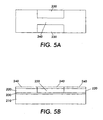
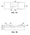
- FIG. 3-8B An exemplary embodiment of a method for fabricating a micro-device, such as the micro-device 100 shown in Fig. 2 , according to this invention is illustrated in Figs. 3-8B . More specifically, Figs. 3-8B are top and cross-sectional views of various exemplary fabrication steps that may be used to fabricate a micro-device including a silicon thermo-optical switch that is at least partially thermally isolated from a substrate.
- the micro-device may be fabricated on a single silicon chip.
- the single silicon chip may comprise a silicon on insulator (SOI) wafer 200 having a silicon substrate 210, a relatively thin single crystal silicon device layer 220 and an insulation layer 230 disposed between the device layer 220 and the substrate 210.
- SOI silicon on insulator
- the wafer 200 may be fabricated using any known or later developed silicon on insulator (SOI) techniques.
- the silicon thermo-optical switch is fabricated in the device layer 220.
- One or more polysilicon layers may be added over the device layer 220 for fabrication of additional mechanical elements, such as hinges, guides, anchors and the like.
- Active electronic elements (not shown), such as electrical traces or logic circuitry, may also be defined in the device layer 220.
- the silicon thermo-optical switch may be fabricated in one of the polysilicon layers formed over the device layer 220.
- a first mask layer 240 such as a photoresist, is formed over the device layer 220.
- the first mask layer 240 may be deposited and patterned using suitable deposition and etching techniques, either known or hereafter developed, to define the silicon thermo-optical switch.
- first mask layer 240 exposed portions of the device layer 220 are etched, for example, using a reactive ion etch (RIE). As shown in Figs. 5A and 5B , the etch is stopped at the insulator layer 230. Then, the first mask layer 240 is removed, as shown in Figs. 6A and 6B , leaving the silicon thermo-optical switch in the device layer 220.
- RIE reactive ion etch
- thermo-optical switch is defined in the device layer 220
- a portion of the insulation layer 230 is removed to form a gap 232, shown in Figs. 8A and 8B .
- the gap 232 formed in the insulation layer 230 at least partially thermally isolates the silicon thermo-optical switch in the device layer 220 from the substrate 210.
- the substrate 210 is to remain intact and unaffected by the removal of the portion of the insulation layer 230 to form the gap 232. If a surface of the substrate 210 is damaged or partially removed with the removal of the portion of the insulation layer 230, important features of the micro-device that may be formed in the substrate 210 may be damaged or lost.
- a second mask layer 250 such as a photoresist, is formed over at least part of the insulation layer 230.
- the second mask layer may also be formed over part or all of the device layer 220 remaining after the above-described etch.
- the second mask layer 250 may be deposited and patterned using suitable deposition and etching techniques, either known or hereafter developed, to define the extent of the gap 232 to be created.
- the etchant is selected so that the exposed portions of the insulation layer 230 are removed without affecting a surface of the substrate 210 underlying the portions of the insulation layer 230 that are removed.
- the selected etchant is highly selective between the materials of the insulation layer 230 and the substrate 210.
- the etchant may be a hydrofluoric acid solution that will attack the silicon dioxide without affecting the silicon during the time required to remove the portions of the insulation layer, typically less than one hour.
- Selectivity will depend on the concentration of the hydrofluoric acid solution, as well as ambient temperature. For example, for a hydrofluoric acid solution at room temperature that is buffered, diluted with water, to have a hydrofluoric acid concentration of 49%, a selectivity of about 50:1 or greater is generally considered to be highly selective according to this invention. However, it is possible to use a selectivity of about 20:1 with an aggressive approach.
- the second mask layer 250 is removed, as shown in Figs. 8A and 8B , leaving a portion of the silicon thermo-optical switch in the device layer 220 that is substantially thermally isolated from the substrate 210 by the gap 232.
- the systems and methods of this invention provide efficient fabrication of the micro-device by avoiding unnecessary steps. For example, selecting an etchant that does not attack the silicon of the substrate 210 avoids the need for a protective layer between the substrate 210 and the insulation layer 230 or the need for a highly controlled etch that removes only a predetermined thickness of the insulation layer 230 so that a partial thickness of the insulation layer remains over the substrate 210 where the gap 232 is formed. Further, since the thermo-optical switch in the device layer 220 is also made of silicon, the selected etchant will not attack the thermo-optical switch. Thus, a protective layer for the thermo-optical switch is not needed.
- the portion of the silicon thermo-optical switch in the device layer 220 that is substantially thermally isolated from the substrate 210 by the gap 232 is substantially stress-free .
- stresses are generated at the silicon-insulation layer (oxide) interfaces.
- the insulation layer 230 is removed at the gap 232, no interface remains that would otherwise induce deformation.
- the oxide coating 6A formed over the rib waveguide 1 and the oxide layer 6 is formed under the rib waveguide 1 will result in undesirable stress in the rib waveguide 1.
- a silicon-oxide interface remains. The oxide layer 6 will tend to buckle the rib waveguide 1 toward or away from the silicon substrate 5 once the rib waveguide is separated from the silicon substrate 5.
Landscapes
- Physics & Mathematics (AREA)
- Engineering & Computer Science (AREA)
- Microelectronics & Electronic Packaging (AREA)
- Nonlinear Science (AREA)
- General Physics & Mathematics (AREA)
- Manufacturing & Machinery (AREA)
- Geometry (AREA)
- Optics & Photonics (AREA)
- Thermal Sciences (AREA)
- Computer Hardware Design (AREA)
- Micromachines (AREA)
- Mechanical Light Control Or Optical Switches (AREA)
- Optical Integrated Circuits (AREA)
- Element Separation (AREA)
Claims (8)
- Verfahren zur Herstellung eines thermo-optischen Schalters, umfassend:Ausbilden eines Substrates (210);Ausbilden einer Isolierschicht (230) über wenigstens einem Teil des Substrates (210),Ausbilden einer Siliziumschicht (220) über wenigstens einem Teil der Isolierschicht (230),Ausbilden einer Siliziumstruktur in der Siliziumschicht (220), wobei die Siliziumstruktur ausgebildet wird, in dem eine erste Maskierschicht über der Siliziumschicht ausgebildet wird und freiliegende Abschnitte der Siliziumschicht geätzt werden; undÄtzen der Isolierschicht (230), um einen Zwischenraum (232) auszubilden, der wenigstens teilweise die Siliziumstruktur vom Substrat (210) thermisch isoliert,wobei das Verfahren dadurch gekennzeichnet ist, dass:die Siliziumstruktur auf vier Armen ruht, die aus der Isolierschicht ausgebildet werden, wobei die Siliziumstruktur erste und zweite Siliziumwellenleiter enthält, die jeweils auf zwei der Armen ruhen;das Verfahren weiterhin das Entfernen der ersten Maskierschicht und Ausbilden einer zweiten Maskierschicht (250) über der Isolierschicht (230) für die Verwendung beim Ätzen der Isolierschicht (230), um so das Ausmaß des Zwischenraumes zu definieren und dadurch die Arme auszubilden, sowie das Entferne der zweiten Maskierschicht enthält;das Ätzmittel eine Selektivität zwischen der Isolierschicht (230) und dem Substrat (210) von wenigstens 20:1 aufweist;und wobei eine Oberfläche des Substrates unter dem Zwischenraum (232) in der Isolierschicht (230) im wesentlichen ungeätzt bleibt.
- Verfahren nach Anspruch 1 bei dem das Ausbilden des Zwischenraumes (232) in der Isolierschicht (230) das Entfernen eines Abschnittes der Isolierschicht mit einem Ätzmittel beinhaltet, das keine Wirkung auf das Substrat (210) hat.
- Verfahren nach Anspruch 1 oder 2, bei dem das Ausbilden des Substrates (210) das Ausbilden eines Siliziumsubstrates und das Entfernen des Abschnittes der Isolierschicht (230) mit einem Ätzmittel beinhaltet, das keine Wirkung auf das Silizium hat.
- Verfahren nach einem der Ansprüche 1 bis 3, bei dem das Ausbilden des Substrates (210) das Ausbilden eines Substrates eines ersten Materials beinhaltet und das Ausbilden der Isolierschicht (230) das Ausbilden einer Schicht eines zweiten Materials beinhaltet.
- Verfahren nach einem der Ansprüche 1 bis 4, bei dem das Ausbilden des Substrates (210) das Ausbilden eines Substrates aus Silizium beinhaltet und das Ausbilden der Isolierschicht (230) das Ausbilden einer Schicht aus einem dielektrischen Material beinhaltet.
- Verfahren nach einem der Ansprüche 1 bis 5, bei dem das Ausbilden des Substrates (210) das Ausbilden eines Substrates aus Silizium beinhaltet und das Ausbilden der Isolierschicht (230) das Ausbilden einer Schicht aus Silizium-Dioxid beinhaltet.
- Verfahren nach einem der Ansprüche 1 bis 6, bei dem das Ätzmittel eine Selektivität zwischen der Isolierschicht (230) und dem Substrat (210) von wenigstens 50:1 hat.
- Verfahren nach einem der Ansprüche 1 bis 7, bei dem das Ausbilden des Zwischenraumes in der Isolierschicht (230) das Entfernen eines Abschnittes der Isolierschicht mit einem Ätzmittel beinhaltet, das keine Wirkung auf die Oberfläche des Substrates (210) hat, das sicht unter dem Zwischenraum befindet.
Applications Claiming Priority (2)
| Application Number | Priority Date | Filing Date | Title |
|---|---|---|---|
| US683533 | 2002-01-16 | ||
| US09/683,533 US6828171B2 (en) | 2002-01-16 | 2002-01-16 | Systems and methods for thermal isolation of a silicon structure |
Publications (3)
| Publication Number | Publication Date |
|---|---|
| EP1333008A2 EP1333008A2 (de) | 2003-08-06 |
| EP1333008A3 EP1333008A3 (de) | 2004-12-08 |
| EP1333008B1 true EP1333008B1 (de) | 2008-11-05 |
Family
ID=24744428
Family Applications (1)
| Application Number | Title | Priority Date | Filing Date |
|---|---|---|---|
| EP03250016A Expired - Lifetime EP1333008B1 (de) | 2002-01-16 | 2003-01-06 | Vorrichtung und Verfahren zur thermischen Isolierung von Siliciumstrukturen |
Country Status (4)
| Country | Link |
|---|---|
| US (1) | US6828171B2 (de) |
| EP (1) | EP1333008B1 (de) |
| JP (2) | JP2003260695A (de) |
| DE (1) | DE60324487D1 (de) |
Families Citing this family (10)
| Publication number | Priority date | Publication date | Assignee | Title |
|---|---|---|---|---|
| US6985651B2 (en) * | 2003-08-05 | 2006-01-10 | Xerox Corporation | Thermal actuator with offset beam segment neutral axes and an optical waveguide switch including the same |
| US6985650B2 (en) * | 2003-08-05 | 2006-01-10 | Xerox Corporation | Thermal actuator and an optical waveguide switch including the same |
| US6983088B2 (en) * | 2003-08-05 | 2006-01-03 | Xerox Corporation | Thermal actuator and an optical waveguide switch including the same |
| JP4422624B2 (ja) * | 2004-03-03 | 2010-02-24 | 日本航空電子工業株式会社 | 微小可動デバイス及びその作製方法 |
| JP2006105651A (ja) * | 2004-10-01 | 2006-04-20 | Ishizuka Electronics Corp | サーモパイル素子及びそれを用いた赤外線センサ |
| JP5130680B2 (ja) * | 2006-03-02 | 2013-01-30 | 日亜化学工業株式会社 | 半導体装置およびその形成方法 |
| US8664050B2 (en) * | 2012-03-20 | 2014-03-04 | International Business Machines Corporation | Structure and method to improve ETSOI MOSFETS with back gate |
| US9957159B2 (en) * | 2016-03-28 | 2018-05-01 | Evigia Systems, Inc. | System and method for an ovenized silicon platform using Si/SiO2 hybrid supports |
| GB2588313B (en) * | 2018-05-11 | 2022-10-05 | Rockley Photonics Ltd | Thermo-optical phase shift with ridged optical waveguide |
| US11921325B2 (en) * | 2020-02-27 | 2024-03-05 | Taiwan Semiconductor Manufacturing Company Limited | Semiconductor device and method of making |
Family Cites Families (21)
| Publication number | Priority date | Publication date | Assignee | Title |
|---|---|---|---|---|
| US4808549A (en) * | 1988-05-27 | 1989-02-28 | Ford Motor Company | Method for fabricating a silicon force transducer |
| US5177661A (en) * | 1989-01-13 | 1993-01-05 | Kopin Corporation | SOI diaphgram sensor |
| FR2700003B1 (fr) * | 1992-12-28 | 1995-02-10 | Commissariat Energie Atomique | Procédé de fabrication d'un capteur de pression utilisant la technologie silicium sur isolant et capteur obtenu. |
| US5508231A (en) * | 1994-03-07 | 1996-04-16 | National Semiconductor Corporation | Apparatus and method for achieving mechanical and thermal isolation of portions of integrated monolithic circuits |
| JP3627761B2 (ja) * | 1994-03-09 | 2005-03-09 | 株式会社デンソー | 半導体力学量センサの製造方法 |
| DE19509868A1 (de) * | 1995-03-17 | 1996-09-19 | Siemens Ag | Mikromechanisches Halbleiterbauelement |
| JP3324395B2 (ja) * | 1995-10-31 | 2002-09-17 | 富士電機株式会社 | 電界型真空管とそれを用いた圧力センサ、加速度センサおよびそれらの製造方法 |
| EP0822578B1 (de) * | 1996-07-31 | 2003-10-08 | STMicroelectronics S.r.l. | Verfahren zur Herstellung von integrierten Halbleiteranordnungen mit chemoresistivem Gasmikrosensor |
| US6472244B1 (en) * | 1996-07-31 | 2002-10-29 | Sgs-Thomson Microelectronics S.R.L. | Manufacturing method and integrated microstructures of semiconductor material and integrated piezoresistive pressure sensor having a diaphragm of polycrystalline semiconductor material |
| DE19644619A1 (de) * | 1996-10-21 | 1998-04-23 | Siemens Ag | Halbleiterkörper mit Heizeinrichtung zum Beeinflussen von Licht |
| US5994816A (en) * | 1996-12-16 | 1999-11-30 | Mcnc | Thermal arched beam microelectromechanical devices and associated fabrication methods |
| US6121552A (en) * | 1997-06-13 | 2000-09-19 | The Regents Of The University Of Caliofornia | Microfabricated high aspect ratio device with an electrical isolation trench |
| GB2320104B (en) | 1997-10-16 | 1998-11-18 | Bookham Technology Ltd | Thermally isolated silicon layer |
| US6329655B1 (en) * | 1998-10-07 | 2001-12-11 | Raytheon Company | Architecture and method of coupling electromagnetic energy to thermal detectors |
| JP2000206476A (ja) * | 1999-01-18 | 2000-07-28 | Kyocera Corp | 温度制御型光導波路 |
| US6094102A (en) * | 1999-04-30 | 2000-07-25 | Rockwell Science Center, Llc | Frequency synthesizer using micro electro mechanical systems (MEMS) technology and method |
| JP2001102597A (ja) * | 1999-09-30 | 2001-04-13 | Fuji Electric Co Ltd | 半導体構造およびその製造方法 |
| US6407851B1 (en) * | 2000-08-01 | 2002-06-18 | Mohammed N. Islam | Micromechanical optical switch |
| JP3573332B2 (ja) * | 2000-02-10 | 2004-10-06 | 日本電信電話株式会社 | 干渉型熱光学光部品 |
| US6356689B1 (en) * | 2000-03-25 | 2002-03-12 | Lucent Technologies, Inc. | Article comprising an optical cavity |
| US6310419B1 (en) * | 2000-04-05 | 2001-10-30 | Jds Uniphase Inc. | Resistor array devices including switch contacts operated by microelectromechanical actuators and methods for fabricating the same |
-
2002
- 2002-01-16 US US09/683,533 patent/US6828171B2/en not_active Expired - Fee Related
-
2003
- 2003-01-06 DE DE60324487T patent/DE60324487D1/de not_active Expired - Lifetime
- 2003-01-06 EP EP03250016A patent/EP1333008B1/de not_active Expired - Lifetime
- 2003-01-09 JP JP2003002748A patent/JP2003260695A/ja active Pending
-
2009
- 2009-07-01 JP JP2009156666A patent/JP5140041B2/ja not_active Expired - Fee Related
Also Published As
| Publication number | Publication date |
|---|---|
| JP5140041B2 (ja) | 2013-02-06 |
| EP1333008A3 (de) | 2004-12-08 |
| US20030134445A1 (en) | 2003-07-17 |
| JP2009214295A (ja) | 2009-09-24 |
| DE60324487D1 (de) | 2008-12-18 |
| JP2003260695A (ja) | 2003-09-16 |
| EP1333008A2 (de) | 2003-08-06 |
| US6828171B2 (en) | 2004-12-07 |
Similar Documents
| Publication | Publication Date | Title |
|---|---|---|
| JP5140041B2 (ja) | シリコン構造熱分離のためのシステム及び方法 | |
| JP2987198B2 (ja) | マイクロ機械的スイッチ | |
| CN100532248C (zh) | 制造具有可动元件的微机电系统的方法 | |
| US7083997B2 (en) | Bonded wafer optical MEMS process | |
| WO2000016041A3 (en) | Formation of suspended beams using soi substrates, and application to the fabrication of a vibrating gyrometer | |
| ATE511493T1 (de) | Verfahren zur herstellung von genauen mikroelektromechanischen strukturen, und so hergestellte mikrostrukturen | |
| JP2007299008A (ja) | 光空洞からなる物品 | |
| JP2003185856A (ja) | モノリシックであって再構築可能な光多重化システム及び光多重化方法 | |
| EP2019081B1 (de) | Bordotierte Ummantelung für MEMS-Vorrichtung | |
| WO2001072631A1 (en) | Fabrication and controlled release of structures using etch-stop trenches | |
| US6761829B2 (en) | Method for fabricating an isolated microelectromechanical system (MEMS) device using an internal void | |
| US7833430B2 (en) | Method for fabricating microstructure and microstructure | |
| EP1252028B1 (de) | Verfahren zum herstellen einer mikromechanisch bearbeiteten struktur | |
| US20040023430A1 (en) | Method for forming a micro-mechanical component in a semiconductor wafer, and a semiconductor wafer comprising a micro-mechanical component formed therein | |
| US6797591B1 (en) | Method for forming a semiconductor device and a semiconductor device formed by the method | |
| KR100727185B1 (ko) | Soi 기판상에서 실리콘 부양구조물의 제조방법 | |
| KR100748741B1 (ko) | 교차 접합된 soi 웨이퍼를 이용한 실리콘 부양구조물의제조방법 | |
| KR100701151B1 (ko) | 미세기전집적시스템용 부양 구조물 제조 방법 | |
| JP2007111831A (ja) | Mems素子の製造方法およびmems素子 | |
| JP2004021030A (ja) | 光マトリクススイッチモジュール及びその製造方法 | |
| JP2004069542A (ja) | 可動部を有する力学量センサの製造方法 | |
| JP2002264095A (ja) | 絶縁体上シリコン及びポリシリコンウェーハの製造方法 |
Legal Events
| Date | Code | Title | Description |
|---|---|---|---|
| PUAI | Public reference made under article 153(3) epc to a published international application that has entered the european phase |
Free format text: ORIGINAL CODE: 0009012 |
|
| AK | Designated contracting states |
Designated state(s): AT BE BG CH CY CZ DE DK EE ES FI FR GB GR HU IE IT LI LU MC NL PT SE SI SK TR |
|
| AX | Request for extension of the european patent |
Extension state: AL LT LV MK RO |
|
| PUAL | Search report despatched |
Free format text: ORIGINAL CODE: 0009013 |
|
| AK | Designated contracting states |
Kind code of ref document: A3 Designated state(s): AT BE BG CH CY CZ DE DK EE ES FI FR GB GR HU IE IT LI LU MC NL PT SE SI SK TR |
|
| AX | Request for extension of the european patent |
Extension state: AL LT LV MK RO |
|
| 17P | Request for examination filed |
Effective date: 20050608 |
|
| AKX | Designation fees paid |
Designated state(s): DE FR GB |
|
| GRAP | Despatch of communication of intention to grant a patent |
Free format text: ORIGINAL CODE: EPIDOSNIGR1 |
|
| GRAS | Grant fee paid |
Free format text: ORIGINAL CODE: EPIDOSNIGR3 |
|
| GRAA | (expected) grant |
Free format text: ORIGINAL CODE: 0009210 |
|
| AK | Designated contracting states |
Kind code of ref document: B1 Designated state(s): DE FR GB |
|
| REG | Reference to a national code |
Ref country code: GB Ref legal event code: FG4D |
|
| REF | Corresponds to: |
Ref document number: 60324487 Country of ref document: DE Date of ref document: 20081218 Kind code of ref document: P |
|
| PLBE | No opposition filed within time limit |
Free format text: ORIGINAL CODE: 0009261 |
|
| STAA | Information on the status of an ep patent application or granted ep patent |
Free format text: STATUS: NO OPPOSITION FILED WITHIN TIME LIMIT |
|
| 26N | No opposition filed |
Effective date: 20090806 |
|
| PGFP | Annual fee paid to national office [announced via postgrant information from national office to epo] |
Ref country code: GB Payment date: 20121224 Year of fee payment: 11 |
|
| PGFP | Annual fee paid to national office [announced via postgrant information from national office to epo] |
Ref country code: FR Payment date: 20130305 Year of fee payment: 11 Ref country code: DE Payment date: 20121226 Year of fee payment: 11 |
|
| REG | Reference to a national code |
Ref country code: DE Ref legal event code: R119 Ref document number: 60324487 Country of ref document: DE |
|
| GBPC | Gb: european patent ceased through non-payment of renewal fee |
Effective date: 20140106 |
|
| REG | Reference to a national code |
Ref country code: DE Ref legal event code: R119 Ref document number: 60324487 Country of ref document: DE Effective date: 20140801 |
|
| PG25 | Lapsed in a contracting state [announced via postgrant information from national office to epo] |
Ref country code: DE Free format text: LAPSE BECAUSE OF NON-PAYMENT OF DUE FEES Effective date: 20140801 |
|
| REG | Reference to a national code |
Ref country code: FR Ref legal event code: ST Effective date: 20140930 |
|
| PG25 | Lapsed in a contracting state [announced via postgrant information from national office to epo] |
Ref country code: FR Free format text: LAPSE BECAUSE OF NON-PAYMENT OF DUE FEES Effective date: 20140131 Ref country code: GB Free format text: LAPSE BECAUSE OF NON-PAYMENT OF DUE FEES Effective date: 20140106 |