EP1333509A2 - Procédé et dispositif pour la production d'energie photovoltaique, basés sur l'emission interne de charges dans une hétérostructure à l'état solide - Google Patents
Procédé et dispositif pour la production d'energie photovoltaique, basés sur l'emission interne de charges dans une hétérostructure à l'état solide Download PDFInfo
- Publication number
- EP1333509A2 EP1333509A2 EP03250444A EP03250444A EP1333509A2 EP 1333509 A2 EP1333509 A2 EP 1333509A2 EP 03250444 A EP03250444 A EP 03250444A EP 03250444 A EP03250444 A EP 03250444A EP 1333509 A2 EP1333509 A2 EP 1333509A2
- Authority
- EP
- European Patent Office
- Prior art keywords
- layer
- electrical power
- state device
- producing electrical
- light according
- Prior art date
- Legal status (The legal status is an assumption and is not a legal conclusion. Google has not performed a legal analysis and makes no representation as to the accuracy of the status listed.)
- Withdrawn
Links
- 238000004519 manufacturing process Methods 0.000 title abstract description 7
- 238000000034 method Methods 0.000 title abstract description 6
- 238000000926 separation method Methods 0.000 claims abstract description 84
- 239000000463 material Substances 0.000 claims abstract description 56
- 230000004888 barrier function Effects 0.000 claims abstract description 44
- 239000004020 conductor Substances 0.000 claims abstract description 44
- 239000002800 charge carrier Substances 0.000 claims abstract description 19
- 239000004065 semiconductor Substances 0.000 claims description 81
- 238000006243 chemical reaction Methods 0.000 claims description 50
- 239000002184 metal Substances 0.000 claims description 32
- 229910052751 metal Inorganic materials 0.000 claims description 31
- GWEVSGVZZGPLCZ-UHFFFAOYSA-N Titan oxide Chemical compound O=[Ti]=O GWEVSGVZZGPLCZ-UHFFFAOYSA-N 0.000 claims description 20
- 239000010409 thin film Substances 0.000 claims description 10
- 239000004408 titanium dioxide Substances 0.000 claims description 10
- 239000010408 film Substances 0.000 claims description 9
- 230000006870 function Effects 0.000 claims description 9
- 239000010931 gold Substances 0.000 claims description 9
- BASFCYQUMIYNBI-UHFFFAOYSA-N platinum Chemical compound [Pt] BASFCYQUMIYNBI-UHFFFAOYSA-N 0.000 claims description 9
- 238000001228 spectrum Methods 0.000 claims description 8
- 238000000576 coating method Methods 0.000 claims description 7
- PCHJSUWPFVWCPO-UHFFFAOYSA-N gold Chemical compound [Au] PCHJSUWPFVWCPO-UHFFFAOYSA-N 0.000 claims description 7
- 229910052737 gold Inorganic materials 0.000 claims description 7
- 239000012212 insulator Substances 0.000 claims description 7
- 229910044991 metal oxide Inorganic materials 0.000 claims description 7
- 239000011248 coating agent Substances 0.000 claims description 6
- SQFDQLBYJKFDDO-UHFFFAOYSA-K merbromin Chemical compound [Na+].[Na+].C=12C=C(Br)C(=O)C=C2OC=2C([Hg]O)=C([O-])C(Br)=CC=2C=1C1=CC=CC=C1C([O-])=O SQFDQLBYJKFDDO-UHFFFAOYSA-K 0.000 claims description 6
- 229960002782 merbromin Drugs 0.000 claims description 6
- 150000004706 metal oxides Chemical class 0.000 claims description 6
- 229910052755 nonmetal Inorganic materials 0.000 claims description 6
- 229920000642 polymer Polymers 0.000 claims description 6
- -1 0-phenylxanthene Chemical compound 0.000 claims description 4
- 239000002086 nanomaterial Substances 0.000 claims description 4
- 229910052697 platinum Inorganic materials 0.000 claims description 4
- 150000002739 metals Chemical class 0.000 claims description 3
- UZUJHVIPEZFEKR-UHFFFAOYSA-L iron(2+);dicyanate Chemical compound [Fe+2].[O-]C#N.[O-]C#N UZUJHVIPEZFEKR-UHFFFAOYSA-L 0.000 claims description 2
- 238000009413 insulation Methods 0.000 claims 3
- QGLKJKCYBOYXKC-UHFFFAOYSA-N nonaoxidotritungsten Chemical compound O=[W]1(=O)O[W](=O)(=O)O[W](=O)(=O)O1 QGLKJKCYBOYXKC-UHFFFAOYSA-N 0.000 claims 3
- BPUBBGLMJRNUCC-UHFFFAOYSA-N oxygen(2-);tantalum(5+) Chemical compound [O-2].[O-2].[O-2].[O-2].[O-2].[Ta+5].[Ta+5] BPUBBGLMJRNUCC-UHFFFAOYSA-N 0.000 claims 3
- 229910001936 tantalum oxide Inorganic materials 0.000 claims 3
- 229910001930 tungsten oxide Inorganic materials 0.000 claims 3
- 150000001913 cyanates Chemical class 0.000 claims 2
- XLJMAIOERFSOGZ-UHFFFAOYSA-M cyanate Chemical compound [O-]C#N XLJMAIOERFSOGZ-UHFFFAOYSA-M 0.000 claims 1
- 239000011810 insulating material Substances 0.000 claims 1
- 238000005381 potential energy Methods 0.000 abstract description 8
- 230000031700 light absorption Effects 0.000 abstract description 4
- 239000010410 layer Substances 0.000 description 93
- 239000003504 photosensitizing agent Substances 0.000 description 16
- 238000012546 transfer Methods 0.000 description 12
- 238000010521 absorption reaction Methods 0.000 description 10
- 239000003638 chemical reducing agent Substances 0.000 description 10
- RTAQQCXQSZGOHL-UHFFFAOYSA-N Titanium Chemical compound [Ti] RTAQQCXQSZGOHL-UHFFFAOYSA-N 0.000 description 7
- 239000003792 electrolyte Substances 0.000 description 7
- 230000003993 interaction Effects 0.000 description 5
- 229920000553 poly(phenylenevinylene) Polymers 0.000 description 5
- 241000894007 species Species 0.000 description 5
- 229910052719 titanium Inorganic materials 0.000 description 5
- 239000010936 titanium Substances 0.000 description 5
- 230000008901 benefit Effects 0.000 description 4
- 239000002131 composite material Substances 0.000 description 4
- 239000011244 liquid electrolyte Substances 0.000 description 4
- 229910052710 silicon Inorganic materials 0.000 description 4
- 239000010703 silicon Substances 0.000 description 4
- 238000013461 design Methods 0.000 description 3
- 238000005516 engineering process Methods 0.000 description 3
- 230000005284 excitation Effects 0.000 description 3
- 238000004770 highest occupied molecular orbital Methods 0.000 description 3
- 230000005525 hole transport Effects 0.000 description 3
- 239000002105 nanoparticle Substances 0.000 description 3
- 230000027756 respiratory electron transport chain Effects 0.000 description 3
- 229910001218 Gallium arsenide Inorganic materials 0.000 description 2
- PXHVJJICTQNCMI-UHFFFAOYSA-N Nickel Chemical compound [Ni] PXHVJJICTQNCMI-UHFFFAOYSA-N 0.000 description 2
- 206010034972 Photosensitivity reaction Diseases 0.000 description 2
- VYPSYNLAJGMNEJ-UHFFFAOYSA-N Silicium dioxide Chemical compound O=[Si]=O VYPSYNLAJGMNEJ-UHFFFAOYSA-N 0.000 description 2
- XLOMVQKBTHCTTD-UHFFFAOYSA-N Zinc monoxide Chemical compound [Zn]=O XLOMVQKBTHCTTD-UHFFFAOYSA-N 0.000 description 2
- 238000002835 absorbance Methods 0.000 description 2
- 239000006096 absorbing agent Substances 0.000 description 2
- 239000011358 absorbing material Substances 0.000 description 2
- UHYPYGJEEGLRJD-UHFFFAOYSA-N cadmium(2+);selenium(2-) Chemical compound [Se-2].[Cd+2] UHYPYGJEEGLRJD-UHFFFAOYSA-N 0.000 description 2
- 150000007942 carboxylates Chemical group 0.000 description 2
- 239000013078 crystal Substances 0.000 description 2
- 230000007547 defect Effects 0.000 description 2
- 238000000151 deposition Methods 0.000 description 2
- 230000008021 deposition Effects 0.000 description 2
- 238000005566 electron beam evaporation Methods 0.000 description 2
- 238000002347 injection Methods 0.000 description 2
- 239000007924 injection Substances 0.000 description 2
- 238000002955 isolation Methods 0.000 description 2
- 229910021421 monocrystalline silicon Inorganic materials 0.000 description 2
- DCZNSJVFOQPSRV-UHFFFAOYSA-N n,n-diphenyl-4-[4-(n-phenylanilino)phenyl]aniline Chemical compound C1=CC=CC=C1N(C=1C=CC(=CC=1)C=1C=CC(=CC=1)N(C=1C=CC=CC=1)C=1C=CC=CC=1)C1=CC=CC=C1 DCZNSJVFOQPSRV-UHFFFAOYSA-N 0.000 description 2
- 239000002245 particle Substances 0.000 description 2
- 230000037361 pathway Effects 0.000 description 2
- 230000001443 photoexcitation Effects 0.000 description 2
- 108091008695 photoreceptors Proteins 0.000 description 2
- 229920003227 poly(N-vinyl carbazole) Polymers 0.000 description 2
- 238000005036 potential barrier Methods 0.000 description 2
- 238000002360 preparation method Methods 0.000 description 2
- 230000008569 process Effects 0.000 description 2
- 238000005215 recombination Methods 0.000 description 2
- 230000006798 recombination Effects 0.000 description 2
- 230000009467 reduction Effects 0.000 description 2
- 239000000243 solution Substances 0.000 description 2
- 238000011282 treatment Methods 0.000 description 2
- ZCYVEMRRCGMTRW-UHFFFAOYSA-N 7553-56-2 Chemical compound [I] ZCYVEMRRCGMTRW-UHFFFAOYSA-N 0.000 description 1
- JAPCXGFREZPNHK-UHFFFAOYSA-N 9-phenyl-9h-xanthene Chemical compound C12=CC=CC=C2OC2=CC=CC=C2C1C1=CC=CC=C1 JAPCXGFREZPNHK-UHFFFAOYSA-N 0.000 description 1
- 239000005083 Zinc sulfide Substances 0.000 description 1
- 229910052782 aluminium Inorganic materials 0.000 description 1
- XAGFODPZIPBFFR-UHFFFAOYSA-N aluminium Chemical compound [Al] XAGFODPZIPBFFR-UHFFFAOYSA-N 0.000 description 1
- VXAUWWUXCIMFIM-UHFFFAOYSA-M aluminum;oxygen(2-);hydroxide Chemical compound [OH-].[O-2].[Al+3] VXAUWWUXCIMFIM-UHFFFAOYSA-M 0.000 description 1
- 229910021417 amorphous silicon Inorganic materials 0.000 description 1
- 238000013459 approach Methods 0.000 description 1
- 238000003491 array Methods 0.000 description 1
- QVGXLLKOCUKJST-UHFFFAOYSA-N atomic oxygen Chemical compound [O] QVGXLLKOCUKJST-UHFFFAOYSA-N 0.000 description 1
- 230000015572 biosynthetic process Effects 0.000 description 1
- 239000000298 carbocyanine Substances 0.000 description 1
- 239000000969 carrier Substances 0.000 description 1
- 239000003795 chemical substances by application Substances 0.000 description 1
- 230000008878 coupling Effects 0.000 description 1
- 238000010168 coupling process Methods 0.000 description 1
- 238000005859 coupling reaction Methods 0.000 description 1
- 238000009792 diffusion process Methods 0.000 description 1
- 230000000694 effects Effects 0.000 description 1
- 230000005611 electricity Effects 0.000 description 1
- 238000004070 electrodeposition Methods 0.000 description 1
- 238000001125 extrusion Methods 0.000 description 1
- AMGQUBHHOARCQH-UHFFFAOYSA-N indium;oxotin Chemical compound [In].[Sn]=O AMGQUBHHOARCQH-UHFFFAOYSA-N 0.000 description 1
- 229910010272 inorganic material Inorganic materials 0.000 description 1
- 239000011147 inorganic material Substances 0.000 description 1
- 229910052740 iodine Inorganic materials 0.000 description 1
- 239000011630 iodine Substances 0.000 description 1
- 239000007788 liquid Substances 0.000 description 1
- 239000007769 metal material Substances 0.000 description 1
- 229910052976 metal sulfide Inorganic materials 0.000 description 1
- 229910003455 mixed metal oxide Inorganic materials 0.000 description 1
- 230000004048 modification Effects 0.000 description 1
- 238000012986 modification Methods 0.000 description 1
- CWQXQMHSOZUFJS-UHFFFAOYSA-N molybdenum disulfide Chemical compound S=[Mo]=S CWQXQMHSOZUFJS-UHFFFAOYSA-N 0.000 description 1
- 229910052759 nickel Inorganic materials 0.000 description 1
- 239000011368 organic material Substances 0.000 description 1
- 150000004866 oxadiazoles Chemical class 0.000 description 1
- 230000003647 oxidation Effects 0.000 description 1
- 238000007254 oxidation reaction Methods 0.000 description 1
- 229910052760 oxygen Inorganic materials 0.000 description 1
- 239000001301 oxygen Substances 0.000 description 1
- 230000000243 photosynthetic effect Effects 0.000 description 1
- 230000000704 physical effect Effects 0.000 description 1
- 239000000049 pigment Substances 0.000 description 1
- QWYZFXLSWMXLDM-UHFFFAOYSA-M pinacyanol iodide Chemical class [I-].C1=CC2=CC=CC=C2N(CC)C1=CC=CC1=CC=C(C=CC=C2)C2=[N+]1CC QWYZFXLSWMXLDM-UHFFFAOYSA-M 0.000 description 1
- 229910021420 polycrystalline silicon Inorganic materials 0.000 description 1
- 229920000123 polythiophene Polymers 0.000 description 1
- 239000002096 quantum dot Substances 0.000 description 1
- 230000005855 radiation Effects 0.000 description 1
- 230000008707 rearrangement Effects 0.000 description 1
- 238000006479 redox reaction Methods 0.000 description 1
- 239000013545 self-assembled monolayer Substances 0.000 description 1
- HBMJWWWQQXIZIP-UHFFFAOYSA-N silicon carbide Chemical compound [Si+]#[C-] HBMJWWWQQXIZIP-UHFFFAOYSA-N 0.000 description 1
- 229910010271 silicon carbide Inorganic materials 0.000 description 1
- 235000012239 silicon dioxide Nutrition 0.000 description 1
- 239000000377 silicon dioxide Substances 0.000 description 1
- 125000006850 spacer group Chemical group 0.000 description 1
- 230000003595 spectral effect Effects 0.000 description 1
- 239000000126 substance Substances 0.000 description 1
- 239000000758 substrate Substances 0.000 description 1
- 239000013589 supplement Substances 0.000 description 1
- 238000004381 surface treatment Methods 0.000 description 1
- 239000000725 suspension Substances 0.000 description 1
- 125000000858 thiocyanato group Chemical group *SC#N 0.000 description 1
- 230000005641 tunneling Effects 0.000 description 1
- 238000007740 vapor deposition Methods 0.000 description 1
- 238000001429 visible spectrum Methods 0.000 description 1
- 235000012431 wafers Nutrition 0.000 description 1
- 239000011787 zinc oxide Substances 0.000 description 1
- 229910052984 zinc sulfide Inorganic materials 0.000 description 1
- DRDVZXDWVBGGMH-UHFFFAOYSA-N zinc;sulfide Chemical compound [S-2].[Zn+2] DRDVZXDWVBGGMH-UHFFFAOYSA-N 0.000 description 1
Images








Classifications
-
- H—ELECTRICITY
- H01—ELECTRIC ELEMENTS
- H01G—CAPACITORS; CAPACITORS, RECTIFIERS, DETECTORS, SWITCHING DEVICES, LIGHT-SENSITIVE OR TEMPERATURE-SENSITIVE DEVICES OF THE ELECTROLYTIC TYPE
- H01G9/00—Electrolytic capacitors, rectifiers, detectors, switching devices, light-sensitive or temperature-sensitive devices; Processes of their manufacture
- H01G9/20—Light-sensitive devices
- H01G9/2027—Light-sensitive devices comprising an oxide semiconductor electrode
- H01G9/2031—Light-sensitive devices comprising an oxide semiconductor electrode comprising titanium oxide, e.g. TiO2
-
- H—ELECTRICITY
- H10—SEMICONDUCTOR DEVICES; ELECTRIC SOLID-STATE DEVICES NOT OTHERWISE PROVIDED FOR
- H10F—INORGANIC SEMICONDUCTOR DEVICES SENSITIVE TO INFRARED RADIATION, LIGHT, ELECTROMAGNETIC RADIATION OF SHORTER WAVELENGTH OR CORPUSCULAR RADIATION
- H10F10/00—Individual photovoltaic cells, e.g. solar cells
- H10F10/10—Individual photovoltaic cells, e.g. solar cells having potential barriers
- H10F10/18—Photovoltaic cells having only Schottky potential barriers
-
- H—ELECTRICITY
- H10—SEMICONDUCTOR DEVICES; ELECTRIC SOLID-STATE DEVICES NOT OTHERWISE PROVIDED FOR
- H10F—INORGANIC SEMICONDUCTOR DEVICES SENSITIVE TO INFRARED RADIATION, LIGHT, ELECTROMAGNETIC RADIATION OF SHORTER WAVELENGTH OR CORPUSCULAR RADIATION
- H10F77/00—Constructional details of devices covered by this subclass
- H10F77/10—Semiconductor bodies
- H10F77/14—Shape of semiconductor bodies; Shapes, relative sizes or dispositions of semiconductor regions within semiconductor bodies
-
- H—ELECTRICITY
- H10—SEMICONDUCTOR DEVICES; ELECTRIC SOLID-STATE DEVICES NOT OTHERWISE PROVIDED FOR
- H10F—INORGANIC SEMICONDUCTOR DEVICES SENSITIVE TO INFRARED RADIATION, LIGHT, ELECTROMAGNETIC RADIATION OF SHORTER WAVELENGTH OR CORPUSCULAR RADIATION
- H10F77/00—Constructional details of devices covered by this subclass
- H10F77/10—Semiconductor bodies
- H10F77/14—Shape of semiconductor bodies; Shapes, relative sizes or dispositions of semiconductor regions within semiconductor bodies
- H10F77/147—Shapes of bodies
-
- H—ELECTRICITY
- H10—SEMICONDUCTOR DEVICES; ELECTRIC SOLID-STATE DEVICES NOT OTHERWISE PROVIDED FOR
- H10K—ORGANIC ELECTRIC SOLID-STATE DEVICES
- H10K30/00—Organic devices sensitive to infrared radiation, light, electromagnetic radiation of shorter wavelength or corpuscular radiation
- H10K30/10—Organic devices sensitive to infrared radiation, light, electromagnetic radiation of shorter wavelength or corpuscular radiation comprising heterojunctions between organic semiconductors and inorganic semiconductors
- H10K30/15—Sensitised wide-bandgap semiconductor devices, e.g. dye-sensitised TiO2
- H10K30/151—Sensitised wide-bandgap semiconductor devices, e.g. dye-sensitised TiO2 the wide bandgap semiconductor comprising titanium oxide, e.g. TiO2
-
- H—ELECTRICITY
- H10—SEMICONDUCTOR DEVICES; ELECTRIC SOLID-STATE DEVICES NOT OTHERWISE PROVIDED FOR
- H10K—ORGANIC ELECTRIC SOLID-STATE DEVICES
- H10K30/00—Organic devices sensitive to infrared radiation, light, electromagnetic radiation of shorter wavelength or corpuscular radiation
- H10K30/354—Organic devices sensitive to infrared radiation, light, electromagnetic radiation of shorter wavelength or corpuscular radiation comprising a metal-insulator-semiconductor [m-i-s] structure
-
- H—ELECTRICITY
- H10—SEMICONDUCTOR DEVICES; ELECTRIC SOLID-STATE DEVICES NOT OTHERWISE PROVIDED FOR
- H10K—ORGANIC ELECTRIC SOLID-STATE DEVICES
- H10K30/00—Organic devices sensitive to infrared radiation, light, electromagnetic radiation of shorter wavelength or corpuscular radiation
- H10K30/50—Photovoltaic [PV] devices
-
- H—ELECTRICITY
- H10—SEMICONDUCTOR DEVICES; ELECTRIC SOLID-STATE DEVICES NOT OTHERWISE PROVIDED FOR
- H10K—ORGANIC ELECTRIC SOLID-STATE DEVICES
- H10K85/00—Organic materials used in the body or electrodes of devices covered by this subclass
- H10K85/10—Organic polymers or oligomers
- H10K85/111—Organic polymers or oligomers comprising aromatic, heteroaromatic, or aryl chains, e.g. polyaniline, polyphenylene or polyphenylene vinylene
- H10K85/114—Poly-phenylenevinylene; Derivatives thereof
-
- H—ELECTRICITY
- H10—SEMICONDUCTOR DEVICES; ELECTRIC SOLID-STATE DEVICES NOT OTHERWISE PROVIDED FOR
- H10K—ORGANIC ELECTRIC SOLID-STATE DEVICES
- H10K85/00—Organic materials used in the body or electrodes of devices covered by this subclass
- H10K85/60—Organic compounds having low molecular weight
- H10K85/649—Aromatic compounds comprising a hetero atom
- H10K85/657—Polycyclic condensed heteroaromatic hydrocarbons
- H10K85/6574—Polycyclic condensed heteroaromatic hydrocarbons comprising only oxygen in the heteroaromatic polycondensed ring system, e.g. cumarine dyes
-
- Y—GENERAL TAGGING OF NEW TECHNOLOGICAL DEVELOPMENTS; GENERAL TAGGING OF CROSS-SECTIONAL TECHNOLOGIES SPANNING OVER SEVERAL SECTIONS OF THE IPC; TECHNICAL SUBJECTS COVERED BY FORMER USPC CROSS-REFERENCE ART COLLECTIONS [XRACs] AND DIGESTS
- Y02—TECHNOLOGIES OR APPLICATIONS FOR MITIGATION OR ADAPTATION AGAINST CLIMATE CHANGE
- Y02E—REDUCTION OF GREENHOUSE GAS [GHG] EMISSIONS, RELATED TO ENERGY GENERATION, TRANSMISSION OR DISTRIBUTION
- Y02E10/00—Energy generation through renewable energy sources
- Y02E10/50—Photovoltaic [PV] energy
- Y02E10/542—Dye sensitized solar cells
-
- Y—GENERAL TAGGING OF NEW TECHNOLOGICAL DEVELOPMENTS; GENERAL TAGGING OF CROSS-SECTIONAL TECHNOLOGIES SPANNING OVER SEVERAL SECTIONS OF THE IPC; TECHNICAL SUBJECTS COVERED BY FORMER USPC CROSS-REFERENCE ART COLLECTIONS [XRACs] AND DIGESTS
- Y02—TECHNOLOGIES OR APPLICATIONS FOR MITIGATION OR ADAPTATION AGAINST CLIMATE CHANGE
- Y02E—REDUCTION OF GREENHOUSE GAS [GHG] EMISSIONS, RELATED TO ENERGY GENERATION, TRANSMISSION OR DISTRIBUTION
- Y02E10/00—Energy generation through renewable energy sources
- Y02E10/50—Photovoltaic [PV] energy
- Y02E10/549—Organic PV cells
-
- Y—GENERAL TAGGING OF NEW TECHNOLOGICAL DEVELOPMENTS; GENERAL TAGGING OF CROSS-SECTIONAL TECHNOLOGIES SPANNING OVER SEVERAL SECTIONS OF THE IPC; TECHNICAL SUBJECTS COVERED BY FORMER USPC CROSS-REFERENCE ART COLLECTIONS [XRACs] AND DIGESTS
- Y02—TECHNOLOGIES OR APPLICATIONS FOR MITIGATION OR ADAPTATION AGAINST CLIMATE CHANGE
- Y02P—CLIMATE CHANGE MITIGATION TECHNOLOGIES IN THE PRODUCTION OR PROCESSING OF GOODS
- Y02P70/00—Climate change mitigation technologies in the production process for final industrial or consumer products
- Y02P70/50—Manufacturing or production processes characterised by the final manufactured product
Definitions
- the present invention is directed to low cost, high efficiency solar cell technology. More specifically, the present invention is related to a method and apparatus for producing photovoltaic energy using solid-state devices.
- Photovoltaic cells convert sunlight directly into electricity by the interaction of photons and electrons within the semiconductor material.
- Most solid-state photovoltaic devices rely on light energy conversion to excite charge carriers (electrons and holes) within a semiconductor material and charge separation by a semiconductor junction producing a potential energy barrier.
- a material such as silicon is doped with atoms from an element with one more or less electrons than occurs in its matching substrate (e.g., silicon).
- a thin layer of each material is joined to form a junction. Photons, striking the cell, transfer their energy to an excited electron hole pair that obtains potential energy. The junction promotes separation of the electrons from the holes thereby preventing recombinations thereof.
- the electrons are collected and caused to flow as a current.
- Various currents and voltages can be supplied through series and parallel arrays of cells.
- the DC current produced depends on the electronic properties of the materials involved and the intensity of the solar radiation incident on the cell.
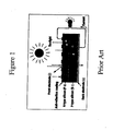
- a conventional solid-state solar cell such as the one shown in Figure 1, may include structures such as a semiconductor junction, heterojunction, interface, and thin-film PV's, which may be made from organic or inorganic materials.
- the necessary elements of these types of devices are a) photon absorption in the semiconductor bulk, b) majority and minority charge carrier transport in the semiconductor bulk, c) a semiconductor band-gap chosen for optimal absorption of the light spectrum and large photovoltages, and d) ideal efficiency limited by open circuit voltages less than the semiconductor band-gap.
- the photon absorption occurs within the bulk semiconductor and both majority and minority carriers are generated and transported in the bulk. For adequate absorbency, relatively thick, high quality semiconductors are needed.
- FIG. 2 Another class of conventional solar cells are the dye-sensitized photoelectrochemical solar cells as shown in Figure 2. These devices were derived from work on photoelectrochemical electron transfer and are cathode/electrolyte/anode systems in which a photoactive molecule is light activated and oxidized (or reduced)by electron (or hole) transfer to the adjacent semiconductor electrode.
- the charge transfer agents which replace the transferred charge in the photoactive molecule are typically molecules or atoms dissolved in a liquid electrolyte such that the molecules or atoms receive charges from an electrode. Reduction is performed by an electron donor in the liquid electrolyte. This device is limited in its power output by the relative free energies of electrons in the electrolyte and the semiconductor which limit the photovoltage.
- the maximum photovoltage is limited by the difference between the bottom of the conduction band edge and the liquid electrolyte chemical potential. Additional inefficiencies result from the required molecular diffusion of the donors to the electrode as well as overpotential losses at the electrode/electrolyte interface.
- Another solid-state solar cell is the dye-sensitized Schottky barrier solar cell as described in U.S. patent nos. 4,105,470 and 4,190,950 by Dr. Skotheim.
- the Skotheim device is similar to the above-mentioned photoelectrochemical cell except the liquid electrolyte is replaced by a "reducing agent" layer, the property of which is not precisely identified in either the '470 nor the '950 patent.
- the preferred embodiment of the present invention described herein is a multilayer solid-state structure wherein light absorption occurs in photosensitive layer (molecules or nanostructures) and the energetic charge carriers produced by the absorption are transported ballistically, without significant energy loss, through an ultra-thin conductor, to and over an adjacent potential energy barrier that separates and stores the charge for use as electrical power.
- the potential energy barrier largely determines the device efficiency and can be optimized by choice of the device materials.
- a photoexcitable molecular species or absorbing nanostructure is deposited on an ultra-thin conductor, and following photoexcitation excited charges are ballistically transported through the conductor to the potential energy barrier (Schottky barrier) created at the interface between the conductor and the charge collection layer (a semiconductor).
- the ultra-thin conductor has, inter alia, three specific functions: I) allows efficient ballistic transport of charge carriers from the photosensitizer to the potential barrier at the interface, II) directly provides replacement charges of the opposite sign to the ionized photosensitizer, and III) influenced, in part, by its interaction with the charge separation layer, the magnitude of the potential energy barrier which determines, in part, the maximum device power.
- the essential components (e.g., layers) of the preferred embodiment of the present invention include: 1) a photosensitive layer where light energy is converted to electron and/or hole excitation, 2) an adjacent ultra-thin conducting layer that provides a pathway for ballistic transport of charges using high efficiency conduction bands, and as a source of replacement charges to the photosensitive layer; and 3) a charge separation and collection layer such as an inorganic or organic semiconductor affixed with a back side ohmic contact opposite the ultra-thin conducting layer. The ohmic contact collects the charges transported across the barrier.
- the addition of an anti-reflection coating on top of the device is a highly practical embodiment of the invention.
- the present invention is advantageous over the aforementioned dye-sensitized Schottky barrier solar cell structure in that it has the advantage of potentially greater photovoltages due to the ability to influence the barrier height by the choice of a high (for n-type semiconductors) or low (for p-type semiconductors) work function conductors at the surface, by the choice of the semiconductor (type and doping level), and by the surface treatment of the semiconductor prior to disposition of the conductor to maximize the barrier height by affecting the interface. Additional advantages of the present invention include eliminating the need for a specific reducing agent or a minority charge carrier transport material, and providing the ability to choose from among a broad choice of charge separation layer material to include both wide band-gap n and p type semiconductors. In contrast to the prior art U.S. patent nos. 4,105,470 and 4,190,950 by Skotheim, only two transfers of electrons to/from conduction bands are required and no intermolecular charge transfer is necessarily required.
- the ultra-thin conductor is used as an efficient ballistic transport channel and to maximize the photovoltage as determined by its effect on the barrier.
- the interaction between the conductor and charge separation layer to influence the barrier height can be optimized by the choice of the conductor, charge separation material, and interface preparation.
- the liquid containing photoelectrochemical cells have reliability and efficiency limits as well as restrictions on the dye stability and reducing agent in solution, thus increasing their in-use costs. Frequently, reactive species such as iodine must be used.
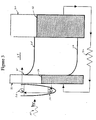
- FIG. 3 illustrates a photosensitized solid-state device in accordance with the preferred embodiment of the present invention. More specifically, the photosensitized solid-state device includes a photosensitive layer 10, a front conducting layer 31, a charge separation layer 39, a back conducting layer 30, and a load 32.
- the front conducting layer 31 is preferably an ultra-thin metal film (preferably in the nanometer range), while the back conducting layer 30 is preferably an ohmic conducting layer.
- the charge separation layer 39 has a determinable conduction band energy level 38 and a determinable valence band energy level 37.
- the metal film may be chemically treated to: 1) allow improved bonding of the photoactive materials, and 2) provide partial isolation of the photoreceptor from the conductor to optimize ballistic charge transfer compared to other pathways to de-excitation of the excited photoreceptor.
- the surface of the device consisting of the photosensitive layer/metal film/charge separation layer is highly contoured, porous, or otherwise shaped to maximize the surface area and maximize the absorbance of photons.
- the front conducting layer 31 and the back conducting layer 30 preferably have determinable work function levels 34 and 33, respectively. It is preferable that the material chosen to make up the front conducting layer 31 has a higher work function (more negative) than the Fermi level of the charge separation layer 39 if the charge separation layer 39 is of an n-type semiconductor, or if the charge separation layer 39 is of a p-type semiconductor, a lower work function to facilitate formation of a Schottky barrier 25.
- the front conducting layer 31 is of the type of material that forms a Schottky barrier with the charge separation layer 39 so as to maximize the power output of the solid-state device.
- Such material may include metals such as gold or platinum, or a non-metal material such as organic conductor polythiophene or a metal oxide.
- materials include low work function conductors including aluminum and titanium.
- the front conducting layer 31 acts as a donor to the photo-oxidized surface species and thereby eliminates the need for a redox active electrolyte, which causes losses in the production of photovoltaic energy and typically has mass transport limitations for current flow.
- the charge separation layer 39 is preferably made of a semiconductor material, or multiple semiconductors.
- Either inorganic semiconductor materials e.g., titanium dioxide, zinc oxide, other metal and mixed metal oxides, moly sulfide, zinc sulfide, other metal and mixed metal sulfides, silicon carbide, etc.
- organic semiconductor materials either hole conducting (e.g., triphenyldiamine (TPD), poly (p-phenylene vinylene) (PPV), poly (vinyl carbazole) (PVC), and their derivatives, etc.), or electron conducting (e.g., conjugated oligothiophenes, oxadiazole derivatives, etc.) may be used.
- TPD triphenyldiamine
- PV poly (p-phenylene vinylene)
- PVC poly (vinyl carbazole)
- electron conducting e.g., conjugated oligothiophenes, oxadiazole derivatives, etc.
- the charge separation layer 39 is made of an insulator or insulator-semiconductor composite structure with the key feature being alignment of the majority carrier bands with the absorber donor level (in Figure 3, 36 for n-type or in Figure 8, 84 for p-type).
- the photosensitizer layer 10 can be a dye or any energy absorbing material or structure, and may include light absorbing atomic or molecular species on a surface (e.g., cis-di(thiocyanato)-N, N-bis-(2,2-bipyridyl-4,4-dicarboxylic acid)-Ru(II), phthalocyanines, carbocyanines, merbromin, 9-phenylxanthene, iron cyanate, etc.), or quantum structures (e.g., nanoparticles of CdS, CdSe, or other semiconductors, or metals, or nanolayers of absorbing material). Additionally, multiple types and/or layers of different photoactive species can be used on the photosensitizer layer 10 to maximize the spectrum capture of incident light. In an alternative embodiment, the photoactive species may be imbedded in the front conductive layer to make a single composite layer.
- the photosensitizer layer, the front and back conducting layers, and the charge separation layer can be deposited by vapor deposition, electrochemical deposition, deposition from solution or colloidal suspension, or be produced by evaporative, extrusion, or other conventional polymer manufacturing techniques.
- the charge separation layer 39 it may be created with high surface area using organic template molecules, or it can be nano-, meso-, or macro-porous to increase the surface area. The conductor and photoactive layers would then follow the contoured surface (see Figure 16).
- a charge separation layer 39 of titanium dioxide is deposited onto titanium foil (the ohmic back contact 30).
- the charge separation layer 39 has a thickness ranging between 100 nm and 500 nm and is deposited by electron beam evaporation and/or by electroanodization of the titanium metal.
- Gold is then deposited to the composite layer to a thickness of 10 nm to form the ultra-thin conductor.
- the preferred embodiment of Figure 3 produces electrical power from a photon energy source based on light energy conversion to charge excitation in a layer containing photosensitive molecules or structures. More specifically, a photon energy source 35 with energy hv, such as sunlight, is incident upon the photosensitive layer 10. The energy source excites electrons 36 located in the photosensitive layer 10 causing the electrons 36 to rise to a higher energy state.
- a photon energy source 35 with energy hv such as sunlight
- ballistic transport refers to the transfer of electrons through a medium in which there is a low or zero scattering cross-section between the electrons and the medium through which they are transferred.
- the process of charge (electron) emission from the photoexcited absorber into and ballistically across the conduction bands of the conductor and charge separation layer is termed "Internal Charge Emission" .
- the electrons travel through the front conducting layer 31, they travel through the charge separation layer 39 towards the back ohmic conducting layer 30 where they are stored with photon derived excess potential energy for later use (dissipation) in passing through the load 32. After losing their energy in the load 32 the electrons are returned to the front conducting layer 31.
- the maximum photovoltage of the device, or open circuit voltage is determined by the potential barrier height between the front conducting layer 31 and the charge separation layer 39. In conventional Schottky solar cells (where the photons are absorbed in the semiconductor band-gap) the same maximum voltage is possible as determined by the barrier height, however, in the present invention the choice of semiconductors is not limited to those with solar spectrum absorbance.
- the voltage can be optimized or influenced by selecting appropriate materials for the front conducting layer 31 and the charge separation layer 39, and by specific treatments of the interface.
- the Schottky barrier varies from approximately 0.4 eV to 0.8 eV as the conductor work function increases from approximately -2.5 eV (Ca) to -5.0 eV (Au) and on GaAs from 0.6 eV (for Mg) to 1 eV (for Pt).
- Preparation of the interface and metal can also be used to increase the barrier for Pd on titanium dioxide where treatment of the metallic conductor Pd with oxygen causes an increase in the barrier of nearly 0.5 eV.
- the design approach is to maximize the barrier and still allow efficient carrier transport across the barrier and efficient replacement of photosensitizer (PS) charge by the conductor.
- PS photosensitizer
- the charge separation layer 39 may be a thin insulating layer (PS-MIM configuration) wherein the conduction band edge and thickness of the insulator are chosen to allow charge carriers from the photoexcited state of the photosensitizer 10 to move to the back contact and prevent current flow in the opposite direction.
- PS-MIM configuration thin insulating layer
- an additional layer of semiconductor is included between the charge separation layer 39 and the back metal contact (PS-MIS configuration).
- the conduction band edge and thickness of the charge separation layer and the semiconductor type are chosen to allow charge carriers from the photoexcited state of the photosensitizer to move to the back contact and prevent current flow in the opposite direction.
- the photosensitizer layer 10 is replaced with a layer of photoactive material 40 comprising of clusters of atoms or molecules, including doped or quantum structures (quantum wells, nanoparticles, quantum dots, etc.), with dimensions engineered to maximize light absorbency and ballistic electron transfer.
- a layer of photoactive material 40 comprising of clusters of atoms or molecules, including doped or quantum structures (quantum wells, nanoparticles, quantum dots, etc.), with dimensions engineered to maximize light absorbency and ballistic electron transfer.
- One advantage of this alternative embodiment is that the charged electrons transferred need not move into or out of an atomic or molecular system, which is the case when using a photosensitive dye. Rather, the electrons travel in and out of degenerate levels with less hindrance due to quantum state restrictions.
- a specific example would be the deposition of CdSe or CdS nanoparticles ( ⁇ 5 nm in dimension) on the conductor surface.
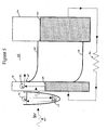
- the electrons 36 of the photosensitizer layer 10 do not ballistically transport through the front conducting layer 31. Rather, as the excited electrons 36 relax back to lower energy states, energy released from electrons 36 excites electrons 50 that reside in the front conducting layer 31. The excited electrons 50 may thereafter rise above the conduction energy band 38 and flow towards the back conducting layer 30.
- the front conducting layer 31 is selected from among either conductors that have transparency characteristics, such as indium tin oxide, or semitransparent conductors (e.g., ultra-thin metal).
- the photosensitizer layer can be deposited between the front conducting layer 31 and the charge separation layer 39, thereby eliminating the need for ballistic transport of the electrons 36, while still maintaining the tenability of the barrier height.
- a doped semiconducting layer 70 having a doping type opposite that of the charge separation layer 39 is placed between the front conducting layer 31 and the charge separation layer 39.
- This particular embodiment effectively increases the Schottky barrier level and thus the open circuit voltage of the photovoltaic device as has been demonstrated in conventional Schottky Barrier Solar Cells.
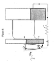
- Figure 8 shows yet another alternative embodiment of the present invention wherein the charge carriers are ballistic holes rather than electrons.
- the above-described operating principles of the preferred embodiment (shown in Figure 3) are symmetrically applied in this instance.
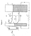
- Figure 9 shows yet another alternative embodiment of the present invention wherein the charge separation layer 39 is made of a material having a narrow band-gap energy level (i.e., the conduction band energy level is close to the valence band energy level).
- the narrow band-gap property of the charge separation layer allows for excitation of additional electrons 90 from the underlying semiconductor material (as in a conventional Schottky diode solar cell).
- the internal emission supplements the photoexcitation of the photosensitizer layer 10 and thereby produces additional energy.
- FIG 10 shows yet another alternative embodiment of the present invention wherein an anti-reflection coating (ARC) layer 100 is added to the photosensitizer layer so as to increase the absorbency of the photosensitizer layer and reduce the reflection of incident light by keeping the photons within the structures.
- ARC anti-reflection coating
- Figure 11 shows a multilayer structure wherein multiple structures of the preferred embodiment as shown in Figure 3 is deposited in a parallel fashion, separated by transparent spacer 112, to produce a superstructure that provides increased absorbency and efficiency in producing photovoltaic energy.
- Figure 11 shows a parallel combination of the preferred embodiment, it should be noted that a serial combination is also possible and feasible.
- Figure 12 shows an alternative embodiment where the absorption of photo energy and injection of electrons may be performed with different molecules or structures. More specifically, the photons are absorbed in one or more photoactive molecules or structures 120 and relay their charge carriers 122 to a second layer or structure 121 with more efficient injection properties. This mimics natural photosynthetic processes whereby multiple pigments are used to more efficiently capture sunlight and relay the excited charges to common collectors for further transport.
- Figure 13 shows an alternative embodiment where absorption occurs in a quantum well 131 deposited on the surface.
- the dimensions of the quantum well and the properties of the material are chosen to optimally inject the charges.
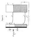
- Figure 14 shows an embodiment where absorption occurs in structure or molecule partially isolated from the conductor to reduce coupling for optimal charge transfer.
- Examples include metal oxides, silicon dioxide, titanium dioxide, aluminum dioxide, organic chains and self-assembled monolayers deposited on the surface prior to the photoabsorber.
- a thin layer of titanium dioxide ⁇ 1-5 nm is deposited on the conductor (Au).
- the photoactive merbromin is applied and forms a covalent linkage through its active carboxylate moiety to the titanium (C-O-Ti).
- a charge separation layer 39 of titanium dioxide is deposited onto titanium foil (the ohmic back contact 30).
- the charge separation layer 39 has a thickness ranging between 100 nm and 500 nm and is deposited by electron beam evaporation and/or by electroanodization of the titanium metal.
- Gold is then deposited to the composite layer to a thickness of 10 nm to form the ultra-thin conductor.
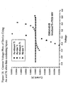
- the resulting current voltage curves of the Schottky contact are shown in Figure 18.
- Also shown in Figure 18 for comparison are devices using nickel instead of gold as the ultra-thin conducting layer 31. An approximately 0.8 eV barrier results.
- Figure 15 shows an alternative embodiment comprising a polymer based device wherein a ballistic hole is injected into an ultra-thin hole carrier.
- Polymer A in Figure 15 e.g., poly(p-phenylene vinylene), PPV
- HOMO occupied molecular orbital
- B in Figure 15 second polymer
- the PPV provides a barrier to reverse hole transport serving the same role as the Schottky barrier. More traditional Schottky barrier devices have also been fabricated from polymer semiconductors and would be configured as in the above embodiments.
Landscapes
- Engineering & Computer Science (AREA)
- Power Engineering (AREA)
- Physics & Mathematics (AREA)
- Electromagnetism (AREA)
- Microelectronics & Electronic Packaging (AREA)
- Chemical & Material Sciences (AREA)
- Inorganic Chemistry (AREA)
- Photovoltaic Devices (AREA)
- Hybrid Cells (AREA)
Applications Claiming Priority (2)
| Application Number | Priority Date | Filing Date | Title |
|---|---|---|---|
| US10/057,223 US6774300B2 (en) | 2001-04-27 | 2002-01-25 | Apparatus and method for photovoltaic energy production based on internal charge emission in a solid-state heterostructure |
| US57223 | 2002-01-25 |
Publications (2)
| Publication Number | Publication Date |
|---|---|
| EP1333509A2 true EP1333509A2 (fr) | 2003-08-06 |
| EP1333509A3 EP1333509A3 (fr) | 2007-08-08 |
Family
ID=22009251
Family Applications (1)
| Application Number | Title | Priority Date | Filing Date |
|---|---|---|---|
| EP03250444A Withdrawn EP1333509A3 (fr) | 2002-01-25 | 2003-01-24 | Procédé et dispositif pour la production d'energie photovoltaique, basés sur l'emission interne de charges dans une hétérostructure à l'état solide |
Country Status (5)
| Country | Link |
|---|---|
| US (4) | US6774300B2 (fr) |
| EP (1) | EP1333509A3 (fr) |
| JP (1) | JP2004040074A (fr) |
| AU (1) | AU2003200122B2 (fr) |
| CA (1) | CA2416213A1 (fr) |
Cited By (4)
| Publication number | Priority date | Publication date | Assignee | Title |
|---|---|---|---|---|
| EP1709690A4 (fr) * | 2004-01-20 | 2009-03-11 | Cyrium Technologies Inc | Cellule solaire comportant une matiere a points quantiques obtenus par croissance epitaxiale |
| RU2415495C2 (ru) * | 2005-12-02 | 2011-03-27 | Хелиантос Б.В. | Фотоэлектрический элемент |
| EP1659639A4 (fr) * | 2003-08-26 | 2011-07-27 | Nippon Oil Corp | Element de conversion photoelectrique |
| US9018515B2 (en) | 2004-01-20 | 2015-04-28 | Cyrium Technologies Incorporated | Solar cell with epitaxially grown quantum dot material |
Families Citing this family (86)
| Publication number | Priority date | Publication date | Assignee | Title |
|---|---|---|---|---|
| US8664030B2 (en) | 1999-03-30 | 2014-03-04 | Daniel Luch | Collector grid and interconnect structures for photovoltaic arrays and modules |
| US6916451B1 (en) * | 1999-05-04 | 2005-07-12 | Neokismet, L.L.C. | Solid state surface catalysis reactor |
| US6678305B1 (en) * | 1999-05-04 | 2004-01-13 | Noekismet, L.L.C. | Surface catalyst infra red laser |
| US7371962B2 (en) | 1999-05-04 | 2008-05-13 | Neokismet, Llc | Diode energy converter for chemical kinetic electron energy transfer |
| US6649823B2 (en) | 1999-05-04 | 2003-11-18 | Neokismet, L.L.C. | Gas specie electron-jump chemical energy converter |
| US7223914B2 (en) * | 1999-05-04 | 2007-05-29 | Neokismet Llc | Pulsed electron jump generator |
| US7005229B2 (en) * | 2002-10-02 | 2006-02-28 | 3M Innovative Properties Company | Multiphoton photosensitization method |
| US7381516B2 (en) * | 2002-10-02 | 2008-06-03 | 3M Innovative Properties Company | Multiphoton photosensitization system |
| US7265161B2 (en) * | 2002-10-02 | 2007-09-04 | 3M Innovative Properties Company | Multi-photon reactive compositions with inorganic particles and method for fabricating structures |
| WO2002058219A2 (fr) | 2001-01-17 | 2002-07-25 | Neokismet, L.L.C. | Convertisseur d'energie chimique a transition electronique |
| US6774300B2 (en) * | 2001-04-27 | 2004-08-10 | Adrena, Inc. | Apparatus and method for photovoltaic energy production based on internal charge emission in a solid-state heterostructure |
| US6657378B2 (en) * | 2001-09-06 | 2003-12-02 | The Trustees Of Princeton University | Organic photovoltaic devices |
| WO2003003469A1 (fr) * | 2001-06-29 | 2003-01-09 | Neokismet, L.L.C. | Procede et appareil d'energisation de puits quantiques |
| US7120411B2 (en) * | 2002-03-25 | 2006-10-10 | Broadcom Corporation | Low noise amplifier (LNA) gain switch circuitry |
| WO2003087564A1 (fr) | 2002-04-11 | 2003-10-23 | Haase Richard A | Procedes, processus, systemes et appareils de la technologie de combustion de l'eau pour la combustion d'hydrogene et d'oxygene |
| DE10239845C1 (de) * | 2002-08-29 | 2003-12-24 | Day4 Energy Inc | Elektrode für fotovoltaische Zellen, fotovoltaische Zelle und fotovoltaischer Modul |
| US7232650B2 (en) * | 2002-10-02 | 2007-06-19 | 3M Innovative Properties Company | Planar inorganic device |
| US6833201B2 (en) | 2003-01-31 | 2004-12-21 | Clemson University | Nanostructured-doped compound for use in an EL element |
| US20080182099A1 (en) * | 2006-11-17 | 2008-07-31 | Jennifer Hoyt Lalli | Robust electrodes for shape memory films |
| US20090087348A1 (en) * | 2007-02-16 | 2009-04-02 | Richard Otto Claus | Sensor applications |
| US20080261044A1 (en) * | 2003-02-10 | 2008-10-23 | Jennifer Hoyt Lalli | Rapidly self-assembled thin films and functional decals |
| US20080213570A1 (en) * | 2007-02-16 | 2008-09-04 | Jennifer Hoyt Lalli | Self-assembled conductive deformable films |
| US20050000565A1 (en) * | 2003-05-22 | 2005-01-06 | Tingying Zeng | Self-assembly methods for the fabrication of McFarland-Tang photovoltaic devices |
| US20060021647A1 (en) * | 2004-07-28 | 2006-02-02 | Gui John Y | Molecular photovoltaics, method of manufacture and articles derived therefrom |
| US7514725B2 (en) * | 2004-11-30 | 2009-04-07 | Spire Corporation | Nanophotovoltaic devices |
| US7306963B2 (en) | 2004-11-30 | 2007-12-11 | Spire Corporation | Precision synthesis of quantum dot nanostructures for fluorescent and optoelectronic devices |
| WO2006110919A2 (fr) * | 2005-04-13 | 2006-10-19 | The Regents Of The University Of California | Multiplication des porteurs de charge dans des matieres semi-conductrices quantiques |
| US7829147B2 (en) * | 2005-08-18 | 2010-11-09 | Corning Incorporated | Hermetically sealing a device without a heat treating step and the resulting hermetically sealed device |
| US20070040501A1 (en) * | 2005-08-18 | 2007-02-22 | Aitken Bruce G | Method for inhibiting oxygen and moisture degradation of a device and the resulting device |
| US20080206589A1 (en) * | 2007-02-28 | 2008-08-28 | Bruce Gardiner Aitken | Low tempertature sintering using Sn2+ containing inorganic materials to hermetically seal a device |
| US7722929B2 (en) * | 2005-08-18 | 2010-05-25 | Corning Incorporated | Sealing technique for decreasing the time it takes to hermetically seal a device and the resulting hermetically sealed device |
| US20070144577A1 (en) * | 2005-12-23 | 2007-06-28 | Rubin George L | Solar cell with physically separated distributed electrical contacts |
| US7498508B2 (en) | 2006-02-24 | 2009-03-03 | Day4 Energy, Inc. | High voltage solar cell and solar cell module |
| US8822810B2 (en) | 2006-04-13 | 2014-09-02 | Daniel Luch | Collector grid and interconnect structures for photovoltaic arrays and modules |
| US9865758B2 (en) | 2006-04-13 | 2018-01-09 | Daniel Luch | Collector grid and interconnect structures for photovoltaic arrays and modules |
| US9006563B2 (en) | 2006-04-13 | 2015-04-14 | Solannex, Inc. | Collector grid and interconnect structures for photovoltaic arrays and modules |
| US8729385B2 (en) | 2006-04-13 | 2014-05-20 | Daniel Luch | Collector grid and interconnect structures for photovoltaic arrays and modules |
| US9236512B2 (en) | 2006-04-13 | 2016-01-12 | Daniel Luch | Collector grid and interconnect structures for photovoltaic arrays and modules |
| US8884155B2 (en) | 2006-04-13 | 2014-11-11 | Daniel Luch | Collector grid and interconnect structures for photovoltaic arrays and modules |
| FR2900052B1 (fr) * | 2006-04-19 | 2011-02-18 | Galderma Sa | Composition comprenant au moins une phase aqueuse et au moins une phase grasse comprenant de l'ivermectine |
| GB0614891D0 (en) * | 2006-07-27 | 2006-09-06 | Univ Southampton | Plasmon-enhanced photo voltaic cell |
| US7985919B1 (en) * | 2006-08-18 | 2011-07-26 | Nanosolar, Inc. | Thermal management for photovoltaic devices |
| US20080047602A1 (en) * | 2006-08-22 | 2008-02-28 | Guardian Industries Corp. | Front contact with high-function TCO for use in photovoltaic device and method of making same |
| US20080047603A1 (en) * | 2006-08-24 | 2008-02-28 | Guardian Industries Corp. | Front contact with intermediate layer(s) adjacent thereto for use in photovoltaic device and method of making same |
| US20080048178A1 (en) * | 2006-08-24 | 2008-02-28 | Bruce Gardiner Aitken | Tin phosphate barrier film, method, and apparatus |
| US8247680B2 (en) | 2006-08-31 | 2012-08-21 | Kabushiki Kaisha Toyota Chuo Kenkyusho | Light energy conversion material |
| US20080092944A1 (en) * | 2006-10-16 | 2008-04-24 | Leonid Rubin | Semiconductor structure and process for forming ohmic connections to a semiconductor structure |
| US20080178932A1 (en) * | 2006-11-02 | 2008-07-31 | Guardian Industries Corp. | Front electrode including transparent conductive coating on patterned glass substrate for use in photovoltaic device and method of making same |
| US8203073B2 (en) * | 2006-11-02 | 2012-06-19 | Guardian Industries Corp. | Front electrode for use in photovoltaic device and method of making same |
| US8076571B2 (en) * | 2006-11-02 | 2011-12-13 | Guardian Industries Corp. | Front electrode for use in photovoltaic device and method of making same |
| US20080105299A1 (en) * | 2006-11-02 | 2008-05-08 | Guardian Industries Corp. | Front electrode with thin metal film layer and high work-function buffer layer for use in photovoltaic device and method of making same |
| US7964788B2 (en) * | 2006-11-02 | 2011-06-21 | Guardian Industries Corp. | Front electrode for use in photovoltaic device and method of making same |
| US8012317B2 (en) * | 2006-11-02 | 2011-09-06 | Guardian Industries Corp. | Front electrode including transparent conductive coating on patterned glass substrate for use in photovoltaic device and method of making same |
| US20080105293A1 (en) * | 2006-11-02 | 2008-05-08 | Guardian Industries Corp. | Front electrode for use in photovoltaic device and method of making same |
| US20080105298A1 (en) * | 2006-11-02 | 2008-05-08 | Guardian Industries Corp. | Front electrode for use in photovoltaic device and method of making same |
| US20080302414A1 (en) * | 2006-11-02 | 2008-12-11 | Den Boer Willem | Front electrode for use in photovoltaic device and method of making same |
| US20160211435A9 (en) | 2007-01-05 | 2016-07-21 | Neokismet, Llc | System and Method for Using Pre-Equilibrium Ballistic Charge Carrier Refraction |
| US7663053B2 (en) * | 2007-01-05 | 2010-02-16 | Neokismet, Llc | System and method for using pre-equilibrium ballistic charge carrier refraction |
| US8334452B2 (en) | 2007-01-08 | 2012-12-18 | Guardian Industries Corp. | Zinc oxide based front electrode doped with yttrium for use in photovoltaic device or the like |
| US20080169021A1 (en) * | 2007-01-16 | 2008-07-17 | Guardian Industries Corp. | Method of making TCO front electrode for use in photovoltaic device or the like |
| US20080206550A1 (en) * | 2007-02-26 | 2008-08-28 | Michael Jeremiah Borlner | Hydrophobic surface |
| US20080223430A1 (en) * | 2007-03-14 | 2008-09-18 | Guardian Industries Corp. | Buffer layer for front electrode structure in photovoltaic device or the like |
| US20090035513A1 (en) * | 2007-03-28 | 2009-02-05 | Michael Jeremiah Bortner | Tethered nanorods |
| US20080245413A1 (en) * | 2007-04-04 | 2008-10-09 | Hang Ruan | Self assembled photovoltaic devices |
| US20080290368A1 (en) * | 2007-05-21 | 2008-11-27 | Day4 Energy, Inc. | Photovoltaic cell with shallow emitter |
| US20080308146A1 (en) * | 2007-06-14 | 2008-12-18 | Guardian Industries Corp. | Front electrode including pyrolytic transparent conductive coating on textured glass substrate for use in photovoltaic device and method of making same |
| WO2009012397A2 (fr) * | 2007-07-18 | 2009-01-22 | The Regents Of The University Of Californina | Dispositif photovoltaïque amélioré par plasmons de surface |
| US20090104434A1 (en) * | 2007-10-17 | 2009-04-23 | Jennifer Hoyt Lalli | Conformal multifunctional coatings |
| US20090104438A1 (en) * | 2007-10-17 | 2009-04-23 | Jennifer Hoyt Lalli | Abrasion resistant coatings |
| US7888594B2 (en) * | 2007-11-20 | 2011-02-15 | Guardian Industries Corp. | Photovoltaic device including front electrode having titanium oxide inclusive layer with high refractive index |
| KR20100097219A (ko) * | 2007-12-18 | 2010-09-02 | 데이4 에너지 인코포레이티드 | Pv 스트링으로 에지 액세스를 수행하는 광전지 모듈, 연결 방법, 장치, 및 시스템 |
| US20090194155A1 (en) * | 2008-02-01 | 2009-08-06 | Guardian Industries Corp. | Front electrode having etched surface for use in photovoltaic device and method of making same |
| US20090194157A1 (en) * | 2008-02-01 | 2009-08-06 | Guardian Industries Corp. | Front electrode having etched surface for use in photovoltaic device and method of making same |
| US8293568B2 (en) * | 2008-07-28 | 2012-10-23 | Day4 Energy Inc. | Crystalline silicon PV cell with selective emitter produced with low temperature precision etch back and passivation process |
| US8022291B2 (en) * | 2008-10-15 | 2011-09-20 | Guardian Industries Corp. | Method of making front electrode of photovoltaic device having etched surface and corresponding photovoltaic device |
| US8502066B2 (en) * | 2009-11-05 | 2013-08-06 | Guardian Industries Corp. | High haze transparent contact including insertion layer for solar cells, and/or method of making the same |
| US20110168252A1 (en) * | 2009-11-05 | 2011-07-14 | Guardian Industries Corp. | Textured coating with etching-blocking layer for thin-film solar cells and/or methods of making the same |
| US20110186120A1 (en) * | 2009-11-05 | 2011-08-04 | Guardian Industries Corp. | Textured coating with various feature sizes made by using multiple-agent etchant for thin-film solar cells and/or methods of making the same |
| TWI394309B (zh) * | 2009-12-30 | 2013-04-21 | Ind Tech Res Inst | 染料敏化太陽能電池 |
| EP2522033B1 (fr) * | 2010-01-08 | 2018-11-14 | TAE Technologies, Inc. | Conversion de photons d'énergie élevée en électricité |
| JP2013541200A (ja) | 2010-09-11 | 2013-11-07 | オレム,ピーター,ミロン | 熱からの電力発生の装置、システム及び方法 |
| US8957298B2 (en) | 2010-09-11 | 2015-02-17 | Peter Milon Orem | Apparatus, systems and methods for electrical power generation from heat |
| JP5789499B2 (ja) * | 2011-11-25 | 2015-10-07 | 株式会社沖データ | レンズアレイ、レンズユニット、ledヘッド、露光装置、画像形成装置及び読取装置 |
| US9437892B2 (en) | 2012-07-26 | 2016-09-06 | Quswami, Inc. | System and method for converting chemical energy into electrical energy using nano-engineered porous network materials |
| JP2014170852A (ja) * | 2013-03-04 | 2014-09-18 | Yoriyasu Ozaki | 光電変換装置及び同装置の製造方法 |
| TWI493739B (zh) * | 2013-06-05 | 2015-07-21 | Univ Nat Taiwan | 熱載子光電轉換裝置及其方法 |
Citations (1)
| Publication number | Priority date | Publication date | Assignee | Title |
|---|---|---|---|---|
| US4442185A (en) * | 1981-10-19 | 1984-04-10 | The United States Of America As Represented By The United States Department Of Energy | Photoelectrochemical cells for conversion of solar energy to electricity and methods of their manufacture |
Family Cites Families (27)
| Publication number | Priority date | Publication date | Assignee | Title |
|---|---|---|---|---|
| US3949463A (en) * | 1973-02-13 | 1976-04-13 | Communications Satellite Corporation (Comsat) | Method of applying an anti-reflective coating to a solar cell |
| US4127738A (en) * | 1976-07-06 | 1978-11-28 | Exxon Research & Engineering Company | Photovoltaic device containing an organic layer |
| US4094751A (en) * | 1976-09-30 | 1978-06-13 | Allied Chemical Corporation | Photochemical diodes |
| US4076904A (en) * | 1976-11-11 | 1978-02-28 | Optel Corporation | Solid state photogalvanic device utilizing sea water as an electrolyte |
| US4105470A (en) | 1977-06-01 | 1978-08-08 | The United States Government As Represented By The United States Department Of Energy | Dye-sensitized schottky barrier solar cells |
| US4190950A (en) | 1977-06-01 | 1980-03-04 | The United States Of America As Represented By The Department Of Energy | Dye-sensitized solar cells |
| US4278830A (en) | 1977-09-29 | 1981-07-14 | Nasa | Schottky barrier solar cell |
| US4342044A (en) * | 1978-03-08 | 1982-07-27 | Energy Conversion Devices, Inc. | Method for optimizing photoresponsive amorphous alloys and devices |
| US4253881A (en) * | 1978-10-23 | 1981-03-03 | Rudolf Hezel | Solar cells composed of semiconductive materials |
| US4278930A (en) * | 1979-09-27 | 1981-07-14 | Gte Automatic Electric Laboratories, Inc. | Current sensing circuit for power supply with series control transistor |
| US4891074A (en) * | 1980-11-13 | 1990-01-02 | Energy Conversion Devices, Inc. | Multiple cell photoresponsive amorphous alloys and devices |
| US4637969A (en) * | 1980-11-18 | 1987-01-20 | Terje Skotheim | Photoelectro-chemical cell for conversion of solar energy to electricity and method of its manufacture |
| DE3234678A1 (de) * | 1982-09-18 | 1984-04-05 | Battelle-Institut E.V., 6000 Frankfurt | Solarzelle |
| DE3536299A1 (de) * | 1985-10-11 | 1987-04-16 | Nukem Gmbh | Solarzelle aus silizium |
| DE3725346A1 (de) * | 1987-07-30 | 1989-02-09 | Nukem Gmbh | Verfahren zur wiederverwendung von silizium-basismaterial einer metall-isolator-halbleiter-(mis)-inversionsschicht-solarzelle |
| US5080725A (en) * | 1987-12-17 | 1992-01-14 | Unisearch Limited | Optical properties of solar cells using tilted geometrical features |
| FR2694451B1 (fr) * | 1992-07-29 | 1994-09-30 | Asulab Sa | Cellule photovoltaïque. |
| US5413739A (en) * | 1992-12-22 | 1995-05-09 | Coleman; James P. | Electrochromic materials and displays |
| JPH11144773A (ja) | 1997-09-05 | 1999-05-28 | Fuji Photo Film Co Ltd | 光電変換素子および光再生型光電気化学電池 |
| US6075203A (en) | 1998-05-18 | 2000-06-13 | E. I. Du Pont Nemours And Company | Photovoltaic cells |
| US6451415B1 (en) * | 1998-08-19 | 2002-09-17 | The Trustees Of Princeton University | Organic photosensitive optoelectronic device with an exciton blocking layer |
| JP2000100483A (ja) * | 1998-09-22 | 2000-04-07 | Sharp Corp | 光電変換素子及びその製造方法及びこれを用いた太陽電池 |
| JP4406985B2 (ja) * | 1999-12-27 | 2010-02-03 | Tdk株式会社 | 酸化物半導体色素結合電極および色素増感型太陽電池 |
| US6570362B1 (en) * | 2000-08-22 | 2003-05-27 | Motorola, Inc. | Portable electronic device with enhanced battery life and cooling |
| US6774300B2 (en) * | 2001-04-27 | 2004-08-10 | Adrena, Inc. | Apparatus and method for photovoltaic energy production based on internal charge emission in a solid-state heterostructure |
| US6580027B2 (en) * | 2001-06-11 | 2003-06-17 | Trustees Of Princeton University | Solar cells using fullerenes |
| US6657378B2 (en) * | 2001-09-06 | 2003-12-02 | The Trustees Of Princeton University | Organic photovoltaic devices |
-
2002
- 2002-01-25 US US10/057,223 patent/US6774300B2/en not_active Expired - Fee Related
-
2003
- 2003-01-13 CA CA002416213A patent/CA2416213A1/fr not_active Abandoned
- 2003-01-14 AU AU2003200122A patent/AU2003200122B2/en not_active Ceased
- 2003-01-24 EP EP03250444A patent/EP1333509A3/fr not_active Withdrawn
- 2003-01-27 JP JP2003017702A patent/JP2004040074A/ja active Pending
- 2003-08-20 US US10/645,747 patent/US6956163B2/en not_active Expired - Fee Related
- 2003-12-31 US US10/750,015 patent/US7087834B2/en not_active Expired - Fee Related
-
2005
- 2005-12-20 US US11/312,018 patent/US20060102227A1/en not_active Abandoned
Patent Citations (1)
| Publication number | Priority date | Publication date | Assignee | Title |
|---|---|---|---|---|
| US4442185A (en) * | 1981-10-19 | 1984-04-10 | The United States Of America As Represented By The United States Department Of Energy | Photoelectrochemical cells for conversion of solar energy to electricity and methods of their manufacture |
Cited By (7)
| Publication number | Priority date | Publication date | Assignee | Title |
|---|---|---|---|---|
| EP1659639A4 (fr) * | 2003-08-26 | 2011-07-27 | Nippon Oil Corp | Element de conversion photoelectrique |
| EP1709690A4 (fr) * | 2004-01-20 | 2009-03-11 | Cyrium Technologies Inc | Cellule solaire comportant une matiere a points quantiques obtenus par croissance epitaxiale |
| AU2005205373B2 (en) * | 2004-01-20 | 2009-09-03 | Cyrium Technologies Incorporated | Solar cell with epitaxially grown quantum dot material |
| AU2005205373B9 (en) * | 2004-01-20 | 2010-06-03 | Cyrium Technologies Incorporated | Solar cell with epitaxially grown quantum dot material |
| US7863516B2 (en) | 2004-01-20 | 2011-01-04 | Cyrium Technologies Incorporated | Solar cell with epitaxially grown quantum dot material |
| US9018515B2 (en) | 2004-01-20 | 2015-04-28 | Cyrium Technologies Incorporated | Solar cell with epitaxially grown quantum dot material |
| RU2415495C2 (ru) * | 2005-12-02 | 2011-03-27 | Хелиантос Б.В. | Фотоэлектрический элемент |
Also Published As
| Publication number | Publication date |
|---|---|
| US20060102227A1 (en) | 2006-05-18 |
| US20030019517A1 (en) | 2003-01-30 |
| US7087834B2 (en) | 2006-08-08 |
| CA2416213A1 (fr) | 2003-07-25 |
| US6774300B2 (en) | 2004-08-10 |
| JP2004040074A (ja) | 2004-02-05 |
| EP1333509A3 (fr) | 2007-08-08 |
| US20050087224A1 (en) | 2005-04-28 |
| US20040154657A1 (en) | 2004-08-12 |
| AU2003200122A1 (en) | 2003-08-14 |
| AU2003200122B2 (en) | 2008-08-21 |
| US6956163B2 (en) | 2005-10-18 |
Similar Documents
| Publication | Publication Date | Title |
|---|---|---|
| US6774300B2 (en) | Apparatus and method for photovoltaic energy production based on internal charge emission in a solid-state heterostructure | |
| EP2174329B1 (fr) | Piles tandem photovoltaiques | |
| US8003884B2 (en) | Photovoltaic device and method for preparing the same | |
| Wei et al. | Photoelectrochemical cell and its applications in optoelectronics | |
| US9123844B2 (en) | Semiconductor grain and oxide layer for photovoltaic cells | |
| US9059418B2 (en) | Method for manufacturing a nanostructured inorganic/organic heterojunction solar cell | |
| US20160218308A1 (en) | Photovoltaic device | |
| US20120312375A1 (en) | All-Solid-State Heterojunction Solar Cell | |
| US20080092946A1 (en) | Semiconductor Grain Microstructures for Photovoltaic Cells | |
| US8158880B1 (en) | Thin-film photovoltaic structures including semiconductor grain and oxide layers | |
| JP2002111031A (ja) | 固体ヘテロ接合および固体増感(感光性)光起電力セル | |
| US20140224329A1 (en) | Devices including organic materials such as singlet fission materials | |
| CN101411001A (zh) | 纳米颗粒敏化的纳米结构的太阳能电池 | |
| Bouclé et al. | Hybrid bulk heterojunction solar cells based on blends of TiO2 nanorods and P3HT | |
| JP4991126B2 (ja) | 積層型有機太陽電池及びその製造方法 | |
| WO1999063599A1 (fr) | Cellule photovoltaique a aspect tandem, nanostructuree et sensible au colorant | |
| Wei et al. | Electrochemical photovoltaic cells—review of recent developments | |
| Kalyanasundaram | Photochemical and photoelectrochemical approaches to energy conversion | |
| Kumar et al. | Photovoltaic application of carbon quantum dots | |
| EP2538452A2 (fr) | Pile solaire à hétérojonction entièrement en semi-conducteurs | |
| Das et al. | Semiconductor Quantum Dot Solar Cells: Construction, Working Principle, and Current Development | |
| Mohd Imran et al. | Applications of Solar Cells | |
| Ahamed et al. | Applications of Solar Cells | |
| David et al. | Role of TiO2 in Highly Efficient Solar Cells | |
| Baruah et al. | Carbon–Science and Technology |
Legal Events
| Date | Code | Title | Description |
|---|---|---|---|
| PUAI | Public reference made under article 153(3) epc to a published international application that has entered the european phase |
Free format text: ORIGINAL CODE: 0009012 |
|
| AK | Designated contracting states |
Designated state(s): AT BE BG CH CY CZ DE DK EE ES FI FR GB GR HU IE IT LI LU MC NL PT SE SI SK TR |
|
| AX | Request for extension of the european patent |
Extension state: AL LT LV MK RO |
|
| RIC1 | Information provided on ipc code assigned before grant |
Ipc: H01L 31/07 20060101ALI20060213BHEP Ipc: H01G 9/20 20060101AFI20060213BHEP |
|
| PUAL | Search report despatched |
Free format text: ORIGINAL CODE: 0009013 |
|
| AK | Designated contracting states |
Kind code of ref document: A3 Designated state(s): AT BE BG CH CY CZ DE DK EE ES FI FR GB GR HU IE IT LI LU MC NL PT SE SI SK TR |
|
| AX | Request for extension of the european patent |
Extension state: AL LT LV MK RO |
|
| 17P | Request for examination filed |
Effective date: 20080129 |
|
| AKX | Designation fees paid |
Designated state(s): AT BE BG CH CY CZ DE DK EE ES FI FR GB GR HU IE IT LI LU MC NL PT SE SI SK TR |
|
| 17Q | First examination report despatched |
Effective date: 20091126 |
|
| STAA | Information on the status of an ep patent application or granted ep patent |
Free format text: STATUS: THE APPLICATION IS DEEMED TO BE WITHDRAWN |
|
| 18D | Application deemed to be withdrawn |
Effective date: 20150801 |