EP1335461A2 - Halbleiterlaser - Google Patents
Halbleiterlaser Download PDFInfo
- Publication number
- EP1335461A2 EP1335461A2 EP03003559A EP03003559A EP1335461A2 EP 1335461 A2 EP1335461 A2 EP 1335461A2 EP 03003559 A EP03003559 A EP 03003559A EP 03003559 A EP03003559 A EP 03003559A EP 1335461 A2 EP1335461 A2 EP 1335461A2
- Authority
- EP
- European Patent Office
- Prior art keywords
- quantum well
- semiconductor laser
- laser device
- layer
- conductivity type
- Prior art date
- Legal status (The legal status is an assumption and is not a legal conclusion. Google has not performed a legal analysis and makes no representation as to the accuracy of the status listed.)
- Withdrawn
Links
- 239000004065 semiconductor Substances 0.000 title claims abstract description 177
- 230000000903 blocking effect Effects 0.000 claims abstract description 75
- 238000005253 cladding Methods 0.000 claims abstract description 74
- 230000003287 optical effect Effects 0.000 claims description 86
- 238000002347 injection Methods 0.000 claims description 51
- 239000007924 injection Substances 0.000 claims description 51
- 230000004888 barrier function Effects 0.000 claims description 18
- 230000000052 comparative effect Effects 0.000 description 27
- 229910001218 Gallium arsenide Inorganic materials 0.000 description 15
- 230000003247 decreasing effect Effects 0.000 description 12
- 238000010586 diagram Methods 0.000 description 12
- 239000000758 substrate Substances 0.000 description 11
- 239000011248 coating agent Substances 0.000 description 8
- 238000000576 coating method Methods 0.000 description 8
- 238000005530 etching Methods 0.000 description 8
- 238000002310 reflectometry Methods 0.000 description 8
- 239000013078 crystal Substances 0.000 description 6
- VYPSYNLAJGMNEJ-UHFFFAOYSA-N Silicium dioxide Chemical compound O=[Si]=O VYPSYNLAJGMNEJ-UHFFFAOYSA-N 0.000 description 4
- 239000000203 mixture Substances 0.000 description 4
- 229910000980 Aluminium gallium arsenide Inorganic materials 0.000 description 3
- YCKRFDGAMUMZLT-UHFFFAOYSA-N Fluorine atom Chemical compound [F] YCKRFDGAMUMZLT-UHFFFAOYSA-N 0.000 description 3
- 229910052731 fluorine Inorganic materials 0.000 description 3
- 239000011737 fluorine Substances 0.000 description 3
- 230000015572 biosynthetic process Effects 0.000 description 2
- 229910052681 coesite Inorganic materials 0.000 description 2
- 238000010276 construction Methods 0.000 description 2
- 229910052906 cristobalite Inorganic materials 0.000 description 2
- 230000001678 irradiating effect Effects 0.000 description 2
- 238000000034 method Methods 0.000 description 2
- 239000000377 silicon dioxide Substances 0.000 description 2
- 229910052682 stishovite Inorganic materials 0.000 description 2
- 229910052905 tridymite Inorganic materials 0.000 description 2
- 229910000530 Gallium indium arsenide Inorganic materials 0.000 description 1
- 238000005229 chemical vapour deposition Methods 0.000 description 1
- 230000000694 effects Effects 0.000 description 1
- 238000005566 electron beam evaporation Methods 0.000 description 1
- 230000020169 heat generation Effects 0.000 description 1
- 239000003550 marker Substances 0.000 description 1
- 239000000463 material Substances 0.000 description 1
- 239000002184 metal Substances 0.000 description 1
- 230000003595 spectral effect Effects 0.000 description 1
- 238000001039 wet etching Methods 0.000 description 1
Images


Classifications
-
- H—ELECTRICITY
- H01—ELECTRIC ELEMENTS
- H01S—DEVICES USING THE PROCESS OF LIGHT AMPLIFICATION BY STIMULATED EMISSION OF RADIATION [LASER] TO AMPLIFY OR GENERATE LIGHT; DEVICES USING STIMULATED EMISSION OF ELECTROMAGNETIC RADIATION IN WAVE RANGES OTHER THAN OPTICAL
- H01S5/00—Semiconductor lasers
- H01S5/30—Structure or shape of the active region; Materials used for the active region
- H01S5/32—Structure or shape of the active region; Materials used for the active region comprising PN junctions, e.g. hetero- or double- heterostructures
- H01S5/3211—Structure or shape of the active region; Materials used for the active region comprising PN junctions, e.g. hetero- or double- heterostructures characterised by special cladding layers, e.g. details on band-discontinuities
- H01S5/3216—Structure or shape of the active region; Materials used for the active region comprising PN junctions, e.g. hetero- or double- heterostructures characterised by special cladding layers, e.g. details on band-discontinuities quantum well or superlattice cladding layers
-
- H—ELECTRICITY
- H01—ELECTRIC ELEMENTS
- H01S—DEVICES USING THE PROCESS OF LIGHT AMPLIFICATION BY STIMULATED EMISSION OF RADIATION [LASER] TO AMPLIFY OR GENERATE LIGHT; DEVICES USING STIMULATED EMISSION OF ELECTROMAGNETIC RADIATION IN WAVE RANGES OTHER THAN OPTICAL
- H01S5/00—Semiconductor lasers
- H01S5/10—Construction or shape of the optical resonator, e.g. extended or external cavity, coupled cavities, bent-guide, varying width, thickness or composition of the active region
- H01S5/16—Window-type lasers, i.e. with a region of non-absorbing material between the active region and the reflecting surface
-
- B—PERFORMING OPERATIONS; TRANSPORTING
- B82—NANOTECHNOLOGY
- B82Y—SPECIFIC USES OR APPLICATIONS OF NANOSTRUCTURES; MEASUREMENT OR ANALYSIS OF NANOSTRUCTURES; MANUFACTURE OR TREATMENT OF NANOSTRUCTURES
- B82Y20/00—Nanooptics, e.g. quantum optics or photonic crystals
-
- H—ELECTRICITY
- H01—ELECTRIC ELEMENTS
- H01S—DEVICES USING THE PROCESS OF LIGHT AMPLIFICATION BY STIMULATED EMISSION OF RADIATION [LASER] TO AMPLIFY OR GENERATE LIGHT; DEVICES USING STIMULATED EMISSION OF ELECTROMAGNETIC RADIATION IN WAVE RANGES OTHER THAN OPTICAL
- H01S3/00—Lasers, i.e. devices using stimulated emission of electromagnetic radiation in the infrared, visible or ultraviolet wave range
- H01S3/14—Lasers, i.e. devices using stimulated emission of electromagnetic radiation in the infrared, visible or ultraviolet wave range characterised by the material used as the active medium
- H01S3/22—Gases
-
- H—ELECTRICITY
- H01—ELECTRIC ELEMENTS
- H01S—DEVICES USING THE PROCESS OF LIGHT AMPLIFICATION BY STIMULATED EMISSION OF RADIATION [LASER] TO AMPLIFY OR GENERATE LIGHT; DEVICES USING STIMULATED EMISSION OF ELECTROMAGNETIC RADIATION IN WAVE RANGES OTHER THAN OPTICAL
- H01S5/00—Semiconductor lasers
- H01S5/10—Construction or shape of the optical resonator, e.g. extended or external cavity, coupled cavities, bent-guide, varying width, thickness or composition of the active region
- H01S5/16—Window-type lasers, i.e. with a region of non-absorbing material between the active region and the reflecting surface
- H01S5/168—Window-type lasers, i.e. with a region of non-absorbing material between the active region and the reflecting surface with window regions comprising current blocking layers
-
- H—ELECTRICITY
- H01—ELECTRIC ELEMENTS
- H01S—DEVICES USING THE PROCESS OF LIGHT AMPLIFICATION BY STIMULATED EMISSION OF RADIATION [LASER] TO AMPLIFY OR GENERATE LIGHT; DEVICES USING STIMULATED EMISSION OF ELECTROMAGNETIC RADIATION IN WAVE RANGES OTHER THAN OPTICAL
- H01S5/00—Semiconductor lasers
- H01S5/30—Structure or shape of the active region; Materials used for the active region
- H01S5/34—Structure or shape of the active region; Materials used for the active region comprising quantum well or superlattice structures, e.g. single quantum well [SQW] lasers, multiple quantum well [MQW] lasers or graded index separate confinement heterostructure [GRINSCH] lasers
-
- H—ELECTRICITY
- H01—ELECTRIC ELEMENTS
- H01S—DEVICES USING THE PROCESS OF LIGHT AMPLIFICATION BY STIMULATED EMISSION OF RADIATION [LASER] TO AMPLIFY OR GENERATE LIGHT; DEVICES USING STIMULATED EMISSION OF ELECTROMAGNETIC RADIATION IN WAVE RANGES OTHER THAN OPTICAL
- H01S5/00—Semiconductor lasers
- H01S5/20—Structure or shape of the semiconductor body to guide the optical wave ; Confining structures perpendicular to the optical axis, e.g. index or gain guiding, stripe geometry, broad area lasers, gain tailoring, transverse or lateral reflectors, special cladding structures, MQW barrier reflection layers
- H01S5/22—Structure or shape of the semiconductor body to guide the optical wave ; Confining structures perpendicular to the optical axis, e.g. index or gain guiding, stripe geometry, broad area lasers, gain tailoring, transverse or lateral reflectors, special cladding structures, MQW barrier reflection layers having a ridge or stripe structure
- H01S5/2205—Structure or shape of the semiconductor body to guide the optical wave ; Confining structures perpendicular to the optical axis, e.g. index or gain guiding, stripe geometry, broad area lasers, gain tailoring, transverse or lateral reflectors, special cladding structures, MQW barrier reflection layers having a ridge or stripe structure comprising special burying or current confinement layers
- H01S5/2206—Structure or shape of the semiconductor body to guide the optical wave ; Confining structures perpendicular to the optical axis, e.g. index or gain guiding, stripe geometry, broad area lasers, gain tailoring, transverse or lateral reflectors, special cladding structures, MQW barrier reflection layers having a ridge or stripe structure comprising special burying or current confinement layers based on III-V materials
-
- H—ELECTRICITY
- H01—ELECTRIC ELEMENTS
- H01S—DEVICES USING THE PROCESS OF LIGHT AMPLIFICATION BY STIMULATED EMISSION OF RADIATION [LASER] TO AMPLIFY OR GENERATE LIGHT; DEVICES USING STIMULATED EMISSION OF ELECTROMAGNETIC RADIATION IN WAVE RANGES OTHER THAN OPTICAL
- H01S5/00—Semiconductor lasers
- H01S5/20—Structure or shape of the semiconductor body to guide the optical wave ; Confining structures perpendicular to the optical axis, e.g. index or gain guiding, stripe geometry, broad area lasers, gain tailoring, transverse or lateral reflectors, special cladding structures, MQW barrier reflection layers
- H01S5/22—Structure or shape of the semiconductor body to guide the optical wave ; Confining structures perpendicular to the optical axis, e.g. index or gain guiding, stripe geometry, broad area lasers, gain tailoring, transverse or lateral reflectors, special cladding structures, MQW barrier reflection layers having a ridge or stripe structure
- H01S5/223—Buried stripe structure
- H01S5/2231—Buried stripe structure with inner confining structure only between the active layer and the upper electrode
-
- H—ELECTRICITY
- H01—ELECTRIC ELEMENTS
- H01S—DEVICES USING THE PROCESS OF LIGHT AMPLIFICATION BY STIMULATED EMISSION OF RADIATION [LASER] TO AMPLIFY OR GENERATE LIGHT; DEVICES USING STIMULATED EMISSION OF ELECTROMAGNETIC RADIATION IN WAVE RANGES OTHER THAN OPTICAL
- H01S5/00—Semiconductor lasers
- H01S5/30—Structure or shape of the active region; Materials used for the active region
- H01S5/32—Structure or shape of the active region; Materials used for the active region comprising PN junctions, e.g. hetero- or double- heterostructures
- H01S5/3202—Structure or shape of the active region; Materials used for the active region comprising PN junctions, e.g. hetero- or double- heterostructures grown on specifically orientated substrates, or using orientation dependent growth
-
- H—ELECTRICITY
- H01—ELECTRIC ELEMENTS
- H01S—DEVICES USING THE PROCESS OF LIGHT AMPLIFICATION BY STIMULATED EMISSION OF RADIATION [LASER] TO AMPLIFY OR GENERATE LIGHT; DEVICES USING STIMULATED EMISSION OF ELECTROMAGNETIC RADIATION IN WAVE RANGES OTHER THAN OPTICAL
- H01S5/00—Semiconductor lasers
- H01S5/30—Structure or shape of the active region; Materials used for the active region
- H01S5/34—Structure or shape of the active region; Materials used for the active region comprising quantum well or superlattice structures, e.g. single quantum well [SQW] lasers, multiple quantum well [MQW] lasers or graded index separate confinement heterostructure [GRINSCH] lasers
- H01S5/3403—Structure or shape of the active region; Materials used for the active region comprising quantum well or superlattice structures, e.g. single quantum well [SQW] lasers, multiple quantum well [MQW] lasers or graded index separate confinement heterostructure [GRINSCH] lasers having a strained layer structure in which the strain performs a special function, e.g. general strain effects, strain versus polarisation
-
- H—ELECTRICITY
- H01—ELECTRIC ELEMENTS
- H01S—DEVICES USING THE PROCESS OF LIGHT AMPLIFICATION BY STIMULATED EMISSION OF RADIATION [LASER] TO AMPLIFY OR GENERATE LIGHT; DEVICES USING STIMULATED EMISSION OF ELECTROMAGNETIC RADIATION IN WAVE RANGES OTHER THAN OPTICAL
- H01S5/00—Semiconductor lasers
- H01S5/30—Structure or shape of the active region; Materials used for the active region
- H01S5/34—Structure or shape of the active region; Materials used for the active region comprising quantum well or superlattice structures, e.g. single quantum well [SQW] lasers, multiple quantum well [MQW] lasers or graded index separate confinement heterostructure [GRINSCH] lasers
- H01S5/343—Structure or shape of the active region; Materials used for the active region comprising quantum well or superlattice structures, e.g. single quantum well [SQW] lasers, multiple quantum well [MQW] lasers or graded index separate confinement heterostructure [GRINSCH] lasers in AIIIBV compounds, e.g. AlGaAs-laser, InP-based laser
- H01S5/34326—Structure or shape of the active region; Materials used for the active region comprising quantum well or superlattice structures, e.g. single quantum well [SQW] lasers, multiple quantum well [MQW] lasers or graded index separate confinement heterostructure [GRINSCH] lasers in AIIIBV compounds, e.g. AlGaAs-laser, InP-based laser with a well layer based on InGa(Al)P, e.g. red laser
Definitions
- the present invention relates generally to semiconductor laser devices, and more particularly, to a semiconductor laser device comprising an active layer having a quantum well structure and an optical recording medium drive using the same.
- An AlGaInP system semiconductor laser device has been actively studied and developed as a semiconductor laser device having a lasing wavelength in a red band.
- the AlGaInP system semiconductor laser device can carry out lasing in a band of 630 to 680 nm, and the wavelength band is high in spectral luminous efficacy. Therefore, the semiconductor laser device is used for a laser pointer, a line marker, and the like.
- the semiconductor laser device has a shorter lasing wavelength than an AlGaAs system semiconductor laser device, whereby it is expected as a light source for high-density recording, for example, and is scheduled to be employed as a light source of a digital video disc (DVD) currently proposed.
- DVD digital video disc
- the inventors of the present application have found that the maximum light output power can be improved to approximately 40 mW by employing a strain compensation type multi quantum well structure for an active layer.
- the semiconductor laser device When the semiconductor laser device is used as a light source for a reloadable optical recording medium, however, it is desired to lengthen the life of the semiconductor laser device while increasing the maximum light output power.
- An object of the present invention is to provide a semiconductor laser device producing high maximum light output power and having a long life.
- Another object of the present invention is to provide an optical recording medium drive comprising a semiconductor laser device producing high maximum light output power and having a long life.
- a semiconductor laser device comprises a cladding layer of a first conductivity type, an active layer having a quantum well structure including one or a plurality of quantum well layers, and a cladding layer of a second conductivity type opposite to the first conductivity type in this order, the cladding layer of the first conductivity type, the active layer, and the cladding layer of the second conductivity type constituting a cavity, further comprising a current injection blocking structure for blocking the injection of current into a region, on the side of at least one of facets of the cavity, of the active layer.
- the semiconductor laser device has the current injection blocking structure in the vicinity of at least one of the facets of the cavity.
- the current injection blocking structure can block the injection of the current into the active layer in the vicinity of the facet of the cavity, whereby heat generation at the facet outputting main laser light can be restrained, so that high output power can be achieved.
- the active layer is substantially a saturable light absorbing member. Consequently, the active layer in a current injection blocking region caused by employing the current injection blocking structure is a loss region before lasing, while being a gain region during lasing.
- the active layer has a quantum well structure, and only the quantum well layer or layers in the quantum well structure will be the saturable light absorbing member, so that the volume of the saturable light absorbing member is decreased. Therefore, lasing threshold current can be prevented from being increased, and the life of the semiconductor laser device can be lengthened.
- the threshold current can be decreased while increasing the maximum light output power, and the life of the semiconductor laser device can be lengthened.
- the current injection blocking structure may comprise a current blocking layer formed on the cladding layer of the second conductivity type and having a stripe-shaped opening for injecting current.
- the stripe-shaped opening may be arranged along the cavity length direction from a position at a predetermined distance from at least one of the facets of the cavity.
- a current injection blocking structure for blocking the injection of current into the active layer is provided on the side of at least one of the facets of the cavity by the current blocking layer having the stripe-shaped opening arranged along the cavity length direction from the position at the predetermined distance from at least one of the facets of the cavity for injecting current. Consequently, the threshold current can be decreased while increasing the maximum light output power, and the life of the semiconductor laser device can be lengthened.
- the cladding layer of the second conductivity type may comprise a flat portion formed on the active layer and a stripe-shaped ridge portion on the flat portion, and the current blocking layer may be formed on the flat portion so as to cover the side surface of the ridge portion and formed on a region on the upper surface of the ridge portion from at least one of the facets of the cavity to the position at the predetermined distance therefrom.
- a current injection blocking structure for blocking the injection of current into the quantum well structure of the active layer is provided on the side of one of the facets of the cavity by the current blocking layer formed on the flat portion so as to cover the side surface of the ridge portion and formed on the region on the upper surface of the ridge portion from one of the facets of the cavity to the position at the predetermined distance therefrom, and a region, where there is provided no current blocking layer, on the upper surface of the ridge portion will be a current injection region. Consequently, the threshold current can be decreased while increasing the maximum light output power, and the life of the semiconductor laser device can be lengthened.
- the total volume of the quantum well layer or layers directly below the stripe-shaped ridge portion is not more than approximately 1 ⁇ 10 -16 m 3 . Consequently, the characteristics of the threshold current and the maximum light output power are good.
- the total volume of the quantum well layer or layers directly below the stripe-shaped ridge portion is not more than approximately 9 ⁇ 10 -17 m 3 . Consequently, the characteristics of the threshold current and the maximum light output power are improved.
- the total volume of the quantum well layer or layers directly below the stripe-shaped ridge portion is not more than approximately 8 ⁇ 10 -17 m 3 . Consequently, the characteristics of the threshold current and the maximum light output power are further improved.
- the total volume of the quantum well layer or layers directly below the stripe-shaped ridge portion is not less than approximately 4 ⁇ 10 -17 m 3 . Consequently, the characteristics of the threshold current and the maximum light output are good.
- the total volume of the quantum well layer or layers directly below the stripe-shaped ridge portion is not less than approximately 4.5 ⁇ 10 -17 m 3 . Consequently, the characteristics of the threshold current and the maximum light output power are improved.
- the total volume of the quantum well layer or layers directly below the stripe-shaped ridge portion is not less than approximately 6 ⁇ 10 -17 m 3 . Consequently, the characteristics of the threshold current and the maximum light output power are further improved.
- the total volume of the quantum well layer or layers directly below the ridge portion is preferably not less than approximately 4 ⁇ 10 -17 m 3 nor more than approximately 1 ⁇ 10 -16 m 3 , more preferably not less than 4.5 ⁇ 10 -17 m 3 nor more than approximately 9 ⁇ 10 -17 m 3 , and still more preferably not less than approximately 6 ⁇ 10 -17 m 3 nor more than approximately 8 ⁇ 10 -17 m 3 .
- the predetermined distance from at least one of the facets of the cavity is not less than approximately 10 ⁇ m nor more than approximately 40 ⁇ m. Consequently, the characteristics of the threshold current and the maximum light output power are improved.
- the predetermined distance from at least one of the facets of the cavity is not less than approximately 20 ⁇ m nor more than approximately 30 ⁇ m. Consequently, the characteristics of the threshold current and the maximum light output power are further improved.
- the semiconductor laser device is composed of an AlGaInP system semiconductor in terms of a short wavelength.
- the cladding layers of the first and second conductivity types may be composed of (Al x1 Ga 1-x1 ) y1 In 1-y1 P
- the quantum well layer may be composed of (Al p Ga 1- p ) q In 1-q P, where 1 ⁇ x1 > 0, 1 > y1 > 0, x1 > p ⁇ 0, and 1 > q > 0.
- the structures are formed on a GaAs semiconductor substrate of the first conductivity type.
- the quantum well structure may be a multi quantum well structure constructed by alternately stacking a plurality of quantum well layers and a plurality of barrier layers. Particularly, it is preferable that the plurality of quantum well layers in the multi quantum well structure have tensile strain, and the plurality of barrier layers therein have compressive strain. In this case, the threshold current can be decreased and the maximum light output power can be increased while achieving a short wavelength, and the life of the semiconductor laser device can be lengthened.
- the plurality of quantum well layers may be composed of (Al p Ga 1-p ) q In 1-q P
- the plurality of barrier layers may be composed of (Al r Ga 1-r ) s In 1-s P, where x1 > p ⁇ 0, 1 > q > 0, 1 ⁇ r > p > 0, and 1 > s > 0.
- the quantum well structure may be a single quantum well structure.
- the volume of the saturable light absorbing member in the active layer can be decreased, whereby the threshold current can be significantly prevented from being increased.
- the quantum well layer in the single quantum well structure may have tensile strain. In this case, a shorter wavelength can be achieved.
- the quantum well layer in the single quantum well structure may be composed of (Al p Ga 1-p ) q In 1-q P, where x1 > p ⁇ 0 and 1 > q > 0.
- the active layer may further comprise optical guide layers provided on both surfaces of the quantum well structure.
- the quantum well layer may have tensile strain, and at least a region, on the side of the quantum well structure, of each of the optical guide layers may have compressive strain.
- the strain of the active layer can be sufficiently compensated for, whereby the life of the semiconductor laser device can be lengthened. Moreover, a short wavelength can be achieved.
- the optical guide layers may be composed of (Al x2 Ga 1-x2 ) y2 In 1-y2 P, where x1 > x2 > 0, and 1 > y2 > 0.
- the current injection blocking structure may be provided in the vicinity of both facets of the cavity.
- a GaAs layer of the first conductivity type may be used as the current blocking layer.
- the cladding layers of the first and second conductivity types may have different compositions.
- the optical guide layers on both surfaces of the quantum well layer may have different compositions.
- An optical recording medium drive comprises a rotation driving portion for rotating an optical recording medium, an optical pickup comprising a semiconductor laser device and a photo detector for irradiating laser light emitted from the semiconductor laser device onto the optical recording medium and receiving returned light from the optical recording medium by the photo detector, a pickup driving portion for moving the optical pickup along the radius of the optical recording medium, and a signal processing portion for processing an output signal from the photo detector in the optical pickup,
- the semiconductor laser device comprising a cladding layer of a first conductivity type, an active layer comprising a quantum well structure including one or a plurality of quantum well layers, and a cladding layer of a second conductivity type opposite to the first conductivity type in this order, the cladding layer of the first conductivity type, the active layer, and the cladding layer of the second conductivity type constituting a cavity, further comprising a current injection blocking structure for blocking the injection of current into a region, on the side of at least one of facets of the cavity, of the active layer.
- the current injection blocking structure may comprise a current blocking layer formed on the cladding layer of the second conductivity type and having a stripe-shaped opening for injecting current.
- the stripe-shaped opening may be arranged along the cavity length direction from a position at a predetermined distance from at least one of the facets of the cavity.
- the cladding layer of the second conductivity type may comprise a flat portion formed on the active layer and a stripe-shaped ridge portion on the flat portion, and the current blocking layer may be formed on the flat portion so as to cover the side surface of the ridge portion and formed on a region on the upper surface of the ridge portion from at least one of the facets of the cavity to the position at the predetermined distance therefrom.
- the semiconductor laser device is composed of an AlGaInP system semiconductor in terms of a short wavelength.
- the cladding layers of the first and second conductivity types maybe composed of (Al x1 Ga 1-x1 ) y1 In 1-y1 P
- the quantum well layer may be composed of (Al p Ga 1- p ) q In 1-q P, where 1 ⁇ x1 > 0, 1 > y1 > 0, x1 > p ⁇ 0, and 1 > q > 0.
- the structures are formed on a GaAs semiconductor substrate of the first conductivity type.
- the quantum well structure may be a multi quantum well structure constructed by alternately stacking a plurality of quantum well layers and a plurality of barrier layers. Particularly, it is preferable that the plurality of quantum well layers in the multi quantum well structure have tensile strain, and the plurality of barrier layers therein have compressive strain.
- the quantum well structure may be a single quantum well structure.
- the quantum well layer in the single quantum well structure may have tensile strain.
- the active layer may further comprise optical guide layers provided on both surfaces of the quantum well structure.
- the quantum well layer may have tensile strain, and at least a region, on the side of the quantum well structure, of each of the optical guide layers may have compressive strain.
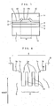
- Fig. 1 is a schematic perspective view of the semiconductor laser device according to the first embodiment
- Fig. 2 is a schematic cross-sectional view taken along a broken line A - A in Fig. 1
- Fig. 3 is a schematic cross-sectional view taken along a broken line B - B in Figs. 1 and 2
- Fig. 4 is a diagram showing a schematic band structure on the side of a conduction band in the vicinity of an active layer of the semiconductor laser device shown in Fig. 1.
- an n-type GaAs semiconductor substrate 1 has one main surface (crystal growth plane) misoriented at an angle ⁇ from the (100) plane to the [011] direction.
- the angle ⁇ is preferably 5 to 17°, and more preferably 7 to 13°, which is 13° in the present embodiment.
- a buffer layer 2 composed of n-type Ga 0.5 In 0.5 P having a thickness of 0.3 ⁇ m is formed on the one main surface of the n-type GaAs semiconductor substrate 1.
- a cladding layer 3 composed of n-type (Al x1 Ga 1- x1 ) y1 In 1-y1 P having a thickness of 1.5 ⁇ m is formed on the buffer layer 2.
- An undoped active layer 4 is formed on the cladding layer 3.
- the active layer 4 has a structure in which an optical guide layer 5, a multi quantum well structure 6 and an optical guide layer 7 are stacked in this order.
- the optical guide layer 5 is composed of undoped (Al x2 Ga 1-x2 ) y2 In 1-y2 P having a thickness of 500 ⁇ .
- x2 0.5.
- the multi quantum well structure 6 has a strain compensation type multi quantum well structure constructed by alternately stacking quantum well layers 6a composed of (Al p Ga 1-p ) q In 1-q P having a thickness of 110 ⁇ which have tensile strain and quantum barrier layers 6b composed of (Al r Ga 1-r ) s In 1-s P having a thickness of 40 ⁇ which have compressive strain, where 1 > p ⁇ 0 and 1 > q > 0.51, and 1 ⁇ r > 0 and 0 ⁇ s ⁇ 0.51.
- the optical guide layer 7 is composed of undoped (Al x2 Ga 1-x2 ) y2 In 1-y2 P having a thickness of 500 ⁇ .
- x2 0.5.
- a flat portion 8 composed of p-type (Al x1 Ga 1- 1 ) y1 In 1-y1 P having a thickness of 0.3 ⁇ m and constituting a p-type cladding layer is formed on the optical guide layer 7.
- An etching stop layer 9 composed of p-type Ga 0.5 In 0.5 P having a thickness of 20 ⁇ is formed on the flat portion 8.
- a stripe-shaped ridge portion 10 composed of p-type (Al x1 Ga 1-x1 ) y1 In 1-y1 P having a width of W5 ⁇ m on its lower surface and having a thickness of 1.2 ⁇ m which extends along the cavity length direction and constituting a p-type cladding layer is formed on the p-type etching stop layer 9.
- x1 0.7
- y1 0.5
- a contact layer 11 composed of p-type Ga 0.5 In 0.5 P having a thickness of 0.1 ⁇ m is formed on the upper surface of the ridge portion 10.
- a current blocking layer 12 composed of n-type GaAs having a thickness of 0.8 ⁇ m is formed on the upper surface of the etching stop layer 9 so as to cover the side surface of the ridge portion 10 and the side surface of the contact layer 11, and is formed on a region on the upper surface of the contact layer 11 from one facet 13a, which outputs main laser light, of a cavity to a position at a predetermined distance L1 therefrom.
- L1 20 ⁇ m.
- the n-type current blocking layer 12 has an opening 12a forming a current path on a region on the upper surface of the contact layer 11 at a distance m from the above-mentioned position at the predetermined distance L1 to the other facet 13b of the cavity, that is, on the upper surface of the ridge portion 10, as shown in Fig. 2.
- a cap layer 14 composed of p-type GaAs having a thickness of 3 ⁇ m is formed on the current blocking layer 12 and the contact layer 11 in the opening 12a.
- a p-side ohmic electrode 15 composed of Au - Cr is formed on the upper surface of the cap layer 14, and an n-side ohmic electrode 16 composed of Au - Sn - Cr is formed on the lower surface of the n-type GaAs semiconductor substrate 1.
- the current blocking layer 12 is formed on the region on the upper surface of the ridge portion 10 from the facet 13a outputting main laser light to the position at the predetermined distance L1 therefrom. Accordingly, a region of the active layer 4 below the current blocking layer 12 is a current injection blocking region into which current is blocked from being injected.
- the current blocking layer 12 is not formed on the region on the upper surface of the ridge portion 10 at a distance m from the above-mentioned position at the predetermined distance L1 to the other facet 13b. Accordingly, the active layer 4 below the region is a current injection region into which current is sufficiently injected. That is, the semiconductor laser device has a current injection blocking structure on the side of one of the facets of the cavity.
- the total volume of the quantum well layers 6a having a width W directly below the stripe-shaped ridge portion 10 is 9.9 ⁇ 10 -17 m 3 .
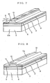
- an n-type buffer layer 2 an n-type cladding layer 3, an undoped active layer 4, a p-type cladding layer 8, a p-type etching stop layer 9, a p-type cladding layer 10, and a p-type contact layer 11 are continuously grown in this order on an n-type GaAs semiconductor substrate 1 by MOCVD (Metal Organic Chemical Vapor Deposition).
- MOCVD Metal Organic Chemical Vapor Deposition
- an SiO 2 film having a thickness of 0.2 ⁇ m is then formed on the p-type contact layer 11 by electron beam evaporation, and the SiO 2 film is patterned by a photolithographic technique and etching using a fluorine etchant, to produce a stripe-shaped mask 21. Thereafter, a region from the p-type contact layer 11 to the p-type etching stop layer 9 is subjected to wet etching with the mask 21 being used, to form the p-type cladding layer 10 in the shape of a stripe-shaped ridge portion.
- the mask 21 from a facet 13a to a position at a predetermined distance L1 therefrom is etched away by a photolithographic technique and etching using a fluorine etchant, as shown in Fig. 7.
- an n-type current blocking layer 12 is then formed by MOCVD with the mask 21 whose portion on the side of the facet 13a is removed being used, after which the mask 21 is etched away by a fluorine etchant.
- a p-type cap layer 14 is then formed by MOCVD, after which a p-side ohmic electrode 15 and an n-side ohmic electrode 16 are formed, to complete the semiconductor laser device shown in Fig. 1.
- the following Table 1 shows a threshold current and maximum light output power in each of the semiconductor laser devices in the present embodiment, a comparative example 1, a comparative example 2 and a comparative example 3.
- the semiconductor laser device in the comparative example 1 is constructed similarly to the semiconductor laser device in the embodiment except that an active layer 4 composed of an undoped (Al 0.15 Ga 0.85 ) 0.5 In 0.5 P layer having a thickness of 800 ⁇ which has no quantum well structure, and there is provided no facet vicinity current injection blocking structure.
- the semiconductor laser device in the comparative example 2 is constructed similarly to the semiconductor laser device in the comparative example 1 except that the above-mentioned facet vicinity current injection blocking layer is provided.
- the semiconductor laser device in the comparative example 3 is constructed similarly to the semiconductor laser device in the embodiment except that the above-mentioned facet vicinity current injection blocking structure is not provided.
- the cavity length L is 600 ⁇ m.
- a coating having reflectivity of 5 % is applied to the facet 13a of the cavity, and a coating having reflectivity of 95 % is applied to the facet 13b of the cavity.
- the maximum light output power can be increased, and the threshold current can be decreased, as compared with those in the semiconductor laser device in the comparative example 1 comprising an active layer having no quantum well structure. That is, the formation of the active layer in the quantum well structure is effective in increasing the maximum light output power and decreasing the threshold current.
- the introduction of the facet vicinity current injection blocking structure increases the threshold current.
- the threshold current is hardly increased, and the maximum light output power can be increased, as compared with those in the semiconductor laser device in the comparative example 3 comprising an active layer having a quantum well structure in which no facet vicinity current injection blocking layer is provided.
- the semiconductor laser device in the present embodiment has a longer life than the semiconductor laser device in the comparative example 3.
- the current injection blocking structure for blocking the injection of current into the active layer 4 is provided in the vicinity of the facet 13a outputting main laser light, and the active layer 4 has the strain compensation type quantum well structure 6 constructed by alternately stacking quantum well layers 6a having tensile strain and quantum barrier layers 6b having compressive strain. Therefore, the maximum light output power can be increased while decreasing the threshold current, and the life of the semiconductor laser device is long.
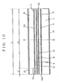
- Fig. 9 is a schematic perspective view of the semiconductor laser device according to the second embodiment
- Fig. 10 is a schematic cross-sectional view taken along a broken line A- A in Fig. 9
- Fig. 11 is a schematic cross-sectional view taken along a broken line B - B in Figs. 9 and 10
- Fig. 12 is a diagram showing a schematic band structure in the vicinity of an active layer of the semiconductor laser device.
- the semiconductor laser device according to the second embodiment differs from the semiconductor laser device according to the first embodiment in that the active layer 4 in the first embodiment is replaced with an active layer 24 having a single quantum well structure. Therefore, the same reference numerals are assigned the same portions as those in the first embodiment and hence, the description thereof is not repeated.
- an undoped active layer 24 is formed on an n-type cladding layer 3.
- the active layer 24 has a structure in which an optical guide layer 25, a single quantum well structure 26 and an optical guide layer 27 are stacked in this order.
- the optical guide layer 25 is composed of undoped (Al x2 Ga 1-x2 ) y2 In 1-y2 P having a thickness of 500 ⁇ .
- x2 0.5.
- y2 0.5 is selected in a region 25b having a thickness of 400 ⁇ on the side of the n-type cladding layer 3, whereby the region 25b has no strain.
- the optical guide layer 27 is composed of undoped (Al x2 Ga 1-x2 ) y2 In 1-y2 P having a thickness of 500 ⁇ .
- x2 0.5.
- the semiconductor laser device is constructed similarly to the semiconductor laser device in the first embodiment except for the structure of the active layer.
- a current blocking layer 12 is formed on a region on the upper surface of a ridge portion 10 from a facet 13a, which outputs main laser light, of a cavity to a position at a predetermined distance L therefrom.
- a region of the active layer 24 below the current blocking layer 12 is a current injection blocking region into which current is blocked from being injected.
- the current blocking layer 12 is not formed on a region on the upper surface of the ridge portion 10 at a distance m from the above-mentioned position at the predetermined distance L1 to the other facet 13b of the cavity.
- the active layer 24 below the region is a current injection region into which current is sufficiently injected. That is, the semiconductor laser device according to the present embodiment has a current injection blocking structure in the vicinity of one of facets of the cavity.
- the total volume of quantum well layer 26a having a width W directly below the stripe-shaped ridge portion 10 is 7.5 ⁇ 10 -17 m 3 .
- the following Table 2 shows threshold current and maximum light output power in each of the semiconductor laser devices in the second embodiment 2 and a comparative example 4.
- the semiconductor laser device in the comparative example 4 is constructed similarly to the semiconductor laser device in the second embodiment except that the above-mentioned facet vicinity current injection region is not provided.
- the cavity length L is 600 ⁇ m.
- a coating having reflectivity of 5 % is applied to the facet 13a of the cavity, and a coating having reflectivity of 95 % is applied to the facet 13b of the cavity.
- the maximum light output power can be increased, and the threshold current can be decreased, as compared with those in the semiconductor laser device in the comparative example 3 comprising an active layer having a multi quantum well structure. That is, the formation of the active layer in the single quantum well structure is significantly effective in increasing the maximum light output power and decreasing the threshold current.
- the threshold current is approximately the same, and the maximum light output power can be increased, as compared with those in the semiconductor laser device in the comparative example 4.
- the threshold current can be decreased, and the maximum light output power can be significantly increased by introducing the facet vicinity current injection blocking structure, as compared with those in the case where the active layer has a multi quantum well structure.
- the semiconductor laser device in the second embodiment has a longer life than those of the semiconductor laser devices in the comparative example 3 and the comparative example 4.
- the relationship between the total volume of the quantum well layers having a width W directly below the ridge portion 10 on the active layer 4 having the facet vicinity current injection blocking structure in the first embodiment, the threshold current, and the maximum light output power is shown in Fig. 13.
- the maximum light output power is measured in a semiconductor laser device in which the reflectivity of a front facet coating of a cavity is 5 % and the reflectivity of a rear facet coating of the cavity is 95 %
- the threshold current is measured in a semiconductor laser device in which both facets of a cavity are uncoated.
- the total volume of the quantum well layers directly below the ridge portion 10 is preferably not more than approximately 1 ⁇ 10 -16 m 3 , more preferably not more than approximately 9 ⁇ 10 -17 m 3 , and still more preferably not more than approximately 8 ⁇ 10 -17 m 3 .
- the characteristics of the threshold current and the maximum light output power are degraded, whereby it is preferably not less than approximately 4 ⁇ 10 -17 m 3 , more preferably not less than approximately 4.5 ⁇ 10 -17 m 3 , and still more preferably not less than approximately 6 ⁇ 10 -17 m 3 nor more than approximately 8 ⁇ 10 -17 m 3 .
- a reliability test of the semiconductor laser devices in the second embodiment and the comparative example 4 is carried out.
- the reflectivity of the front facet coating of the cavity is taken as 5 %
- the reflectivity of the rear facet coating of the cavity is taken as 95 %
- the cavity length L is taken as 600 ⁇ m
- the light output power is taken as 30 mW, to measure the change in an operating current at a temperature of 50°C.
- the semiconductor laser device in the comparative example 4 As shown in Fig. 14, in the semiconductor laser device in the comparative example 4, the operating current is raised beyond 100 hours. On the other hand, in the semiconductor laser device in the second embodiment 2, the operating current is hardly raised even beyond 1000 hours. It is thus found that the semiconductor laser device in the second embodiment has a longer life than the semiconductor laser device in the comparative example 4.
- the distance L1 is 20 ⁇ m
- approximately the same superior characteristics are obtained when the distance L1 is 20 to 30 ⁇ m, and a good effect is also obtained if it is in the range of approximately 10 to approximately 40 ⁇ m.
- the active layer may have a quantum well structure having tensile strain or compressive strain, or may have a quantum well structure having no strain.
- the active layer has the strain compensation type quantum well structure in order that the threshold current is low and the maximum light output power is high in a short wavelength region, and the life of the semiconductor laser device is long.
- the n-type Ga 0.5 In 0.5 P buffer layer 2 provided between the n-type GaAs semiconductor substrate 1 and the n-type cladding layer 3 may be replaced with an n-type GaAs buffer layer.
- no buffer layer may be provided.
- a structure in which the etching stop layer 9 is not used can be also realized.
- the current injection blocking structure is provided in the vicinity of one of the facets of the cavity
- the current injection blocking structure may be provided in the vicinity of both the facets of the cavity.
- the GaAs semiconductor substrate 1 has one main surface (crystal growth plane) misoriented from the (100) surface to the [011] direction, it is desirable that the GaAs semiconductor substrate has one main surface (crystal growth plane) in an equivalent relation therewith.
- one main surface (crystal growth plane) of the GaAs semiconductor substrate may be a plane misoriented from the (100) surface to the [0 1 1 ] direction, a plane misoriented from the (010) surface to the [101] or [ 1 0 1 ] direction, or a plane misoriented from the (001) surface to the [110] or [ 1 1 0] direction, that is, a plane misoriented from the ⁇ 100 ⁇ plane to the ⁇ 011> direction.
- the present invention is applicable to a semiconductor laser device comprising a current blocking layer having a stripe-shaped opening, for example, a self-alignment type semiconductor laser device.
- a semiconductor laser device comprising a current blocking layer having a stripe-shaped opening
- a self-alignment type semiconductor laser device for example, a self-alignment type semiconductor laser device.
- the AlGaInP type semiconductor laser device the present invention is also applicable to a semiconductor device of another material system, for example, an AlGaAs system, GaInAsP system, GaInAs system, ZnMgSSe system and AlInGaN system semiconductor laser devices.
- Fig. 15 is a schematic view of an optical pickup 100 using the semiconductor laser device according to the present invention.
- laser light emitted from a semiconductor laser device 31 passes through a diffraction grating 32, a beam splitter 33, and a collimator lens 34, and is converged on the surface of an optical disk LD by an objective lens 36 having an aperture stop 35.
- Returned light from the optical disk LD passes through the objective lens 36 and the collimator lens 34, is reflected by the beam splitter 33, and is incident on a photodiode 39 through a concave lens 37 and a cylindrical lens 38.
- Fig. 16 is a block diagram showing the construction of an optical recording medium drive 200 using the optical pickup 100 shown in Fig. 15.
- the optical recording medium drive 200 shown in Fig. 16 is an optical disk drive for reading information from an optical disk LD.
- the optical recording medium drive 200 comprises an optical pickup 100, a motor 101, a rotation control system 102, a coarse motor 103, a coarse motor control system 104, a pickup control system 105, a signal processing system 106, and a drive controller 107.
- the motor 101 rotates the optical disk LD at a predetermined speed.
- the rotation control system 102 controls a rotating operation of the motor 101.
- the coarse motor 103 moves the optical pickup 100 along the radius of the optical disk LD.
- the coarse motor control system 104 controls operations performed by the coarse motor 103.
- the optical pickup 100 irradiates laser light onto the optical disk LD, and receives returned light from the optical disk LD.
- the pickup control system 105 controls a projecting and receiving operation of the optical pickup 100.
- the signal processing system 106 calculates a reproduction signal, a focus error signal and a tracking error signal upon receipt of an output signal from a photodiode 39 in the optical pickup 100, and feeds the reproduction signal to the drive controller 107, while feeding the focus error signal and the tracking error signal to the pickup control system 105.
- the drive controller 107 controls the rotation control system 102, the coarse motor control system 104, the pickup control system 105 and the signal processing system 106 in conformity to a command given through a drive interface 108, and outputs the reproduction signal through the drive interface 108.
- the semiconductor laser device according to the present invention is used, whereby reliable and high-density recording and reproduction of information are possible with low power consumption, and the life of products is lengthened.
- the semiconductor laser device of the present invention can be used for optical pickups having different structures from the optical pickup shown in Fig.15 and optical recording medium drives having different structures from the optical recording medium drive shown in Fig.16.
Landscapes
- Physics & Mathematics (AREA)
- Electromagnetism (AREA)
- Optics & Photonics (AREA)
- General Physics & Mathematics (AREA)
- Condensed Matter Physics & Semiconductors (AREA)
- Engineering & Computer Science (AREA)
- Nanotechnology (AREA)
- Chemical & Material Sciences (AREA)
- Plasma & Fusion (AREA)
- Crystallography & Structural Chemistry (AREA)
- Biophysics (AREA)
- Life Sciences & Earth Sciences (AREA)
- Geometry (AREA)
- Semiconductor Lasers (AREA)
Applications Claiming Priority (3)
| Application Number | Priority Date | Filing Date | Title |
|---|---|---|---|
| JP23679896 | 1996-09-06 | ||
| JP23679896 | 1996-09-06 | ||
| EP97306901A EP0828324B1 (de) | 1996-09-06 | 1997-09-05 | Halbleiterlaservorrichtung |
Related Parent Applications (1)
| Application Number | Title | Priority Date | Filing Date |
|---|---|---|---|
| EP97306901A Division EP0828324B1 (de) | 1996-09-06 | 1997-09-05 | Halbleiterlaservorrichtung |
Publications (2)
| Publication Number | Publication Date |
|---|---|
| EP1335461A2 true EP1335461A2 (de) | 2003-08-13 |
| EP1335461A3 EP1335461A3 (de) | 2004-09-15 |
Family
ID=17005955
Family Applications (2)
| Application Number | Title | Priority Date | Filing Date |
|---|---|---|---|
| EP97306901A Expired - Lifetime EP0828324B1 (de) | 1996-09-06 | 1997-09-05 | Halbleiterlaservorrichtung |
| EP03003559A Withdrawn EP1335461A3 (de) | 1996-09-06 | 1997-09-05 | Halbleiterlaser |
Family Applications Before (1)
| Application Number | Title | Priority Date | Filing Date |
|---|---|---|---|
| EP97306901A Expired - Lifetime EP0828324B1 (de) | 1996-09-06 | 1997-09-05 | Halbleiterlaservorrichtung |
Country Status (5)
| Country | Link |
|---|---|
| US (1) | US6044099A (de) |
| EP (2) | EP0828324B1 (de) |
| KR (1) | KR100539354B1 (de) |
| CN (1) | CN1159811C (de) |
| DE (1) | DE69723009T2 (de) |
Families Citing this family (6)
| Publication number | Priority date | Publication date | Assignee | Title |
|---|---|---|---|---|
| EP1130722B1 (de) * | 1999-12-28 | 2007-02-14 | Sanyo Electric Co., Ltd. | Halbleiterlaservorrichtung |
| JP2003086886A (ja) * | 2001-07-02 | 2003-03-20 | Sharp Corp | 半導体レーザ装置およびその製造方法 |
| KR100495220B1 (ko) * | 2003-06-25 | 2005-06-14 | 삼성전기주식회사 | 고차모드 흡수층을 갖는 반도체 레이저 다이오드 |
| CN102037575B (zh) * | 2008-03-27 | 2013-04-10 | 宋俊午 | 发光元件及其制造方法 |
| US9093820B1 (en) * | 2011-01-25 | 2015-07-28 | Soraa Laser Diode, Inc. | Method and structure for laser devices using optical blocking regions |
| CN117080867A (zh) * | 2022-05-10 | 2023-11-17 | 鸿海精密工业股份有限公司 | 纳米晶体阵列、激光器件及显示装置 |
Citations (1)
| Publication number | Priority date | Publication date | Assignee | Title |
|---|---|---|---|---|
| US5396508A (en) * | 1992-09-22 | 1995-03-07 | Xerox Corporation | Polarization switchable quantum well laser |
Family Cites Families (15)
| Publication number | Priority date | Publication date | Assignee | Title |
|---|---|---|---|---|
| GB2222307B (en) * | 1988-07-22 | 1992-04-01 | Mitsubishi Electric Corp | Semiconductor laser |
| JPH07101768B2 (ja) * | 1988-11-09 | 1995-11-01 | 三菱電機株式会社 | 半導体レーザ装置及びその製造方法 |
| JPH02148786A (ja) * | 1988-11-29 | 1990-06-07 | Sanyo Electric Co Ltd | 半導体レーザ装置 |
| JP2823228B2 (ja) * | 1988-11-29 | 1998-11-11 | 三洋電機株式会社 | 半導体レーザ装置及びその製造方法 |
| US5181218A (en) * | 1988-12-14 | 1993-01-19 | Kabushiki Kaisha Toshiba | Manufacturing method of semiconductor laser with non-absorbing mirror structure |
| JPH02203586A (ja) * | 1989-02-01 | 1990-08-13 | Mitsubishi Electric Corp | 半導体レーザ装置とその製造方法 |
| JPH03208388A (ja) * | 1990-01-09 | 1991-09-11 | Nec Corp | 半導体レーザ及びその製造方法と不純物拡散方法 |
| US5235581A (en) * | 1990-08-09 | 1993-08-10 | Matsushita Electric Industrial Co., Ltd. | Optical recording/reproducing apparatus for optical disks with various disk substrate thicknesses |
| JP3242955B2 (ja) * | 1991-10-21 | 2001-12-25 | 株式会社東芝 | 半導体レーザ装置 |
| US5600667A (en) * | 1993-04-05 | 1997-02-04 | Matsushita Electric Industrial Co., Ltd. | Semiconductor laser device |
| TW238381B (en) * | 1993-10-29 | 1995-01-11 | Ibm | Optical data storage cartridge system |
| US5559818A (en) * | 1994-03-24 | 1996-09-24 | Sanyo Electric Co., Ltd. | Semiconductor laser device |
| EP0675488B1 (de) * | 1994-03-30 | 2000-05-17 | Mitsumi Electric Company Ltd. | Aufzeichnungs- und Antriebsgerät für optische Scheiben |
| JPH08138901A (ja) * | 1994-11-08 | 1996-05-31 | Furukawa Electric Co Ltd:The | 半導体レーザ素子 |
| JP4011640B2 (ja) * | 1995-03-02 | 2007-11-21 | 三菱電機株式会社 | 半導体レーザ,及び半導体レーザの製造方法 |
-
1997
- 1997-09-05 KR KR1019970045931A patent/KR100539354B1/ko not_active Expired - Fee Related
- 1997-09-05 EP EP97306901A patent/EP0828324B1/de not_active Expired - Lifetime
- 1997-09-05 EP EP03003559A patent/EP1335461A3/de not_active Withdrawn
- 1997-09-05 DE DE69723009T patent/DE69723009T2/de not_active Expired - Lifetime
- 1997-09-05 US US08/924,826 patent/US6044099A/en not_active Expired - Lifetime
- 1997-09-08 CN CNB971184488A patent/CN1159811C/zh not_active Expired - Fee Related
Patent Citations (1)
| Publication number | Priority date | Publication date | Assignee | Title |
|---|---|---|---|---|
| US5396508A (en) * | 1992-09-22 | 1995-03-07 | Xerox Corporation | Polarization switchable quantum well laser |
Non-Patent Citations (5)
| Title |
|---|
| ARIMOTO S ET AL: "150 mW fundamental-transverse-mode operation of 670 nm window laser diode", IEEE JOURNAL OF QUANTUM ELECTRONICS USA, vol. 29, no. 6, June 1993 (1993-06-01), pages 1874 - 1879, XP000397627, ISSN: 0018-9197, DOI: 10.1109/3.234447 * |
| BESSHO Y ET AL: "Self-pulsating 630 nm band strain-compensated MQW AlGaInP laser diodes", ELECTRONICS LETTERS, IEE STEVENAGE, GB, vol. 32, no. 7, 28 March 1996 (1996-03-28), pages 667 - 668, XP006004968, ISSN: 0013-5194, DOI: 10.1049/EL:19960457 * |
| KOBAYASHI R ET AL: "Low-threshold, highly reliable 630 nm-band AlGaIP visible laser diodes with AlInP buried waveguide", ELECTRONICS LETTERS, IEE STEVENAGE, GB, vol. 32, no. 10, 9 May 1996 (1996-05-09), pages 894 - 896, XP006005117, ISSN: 0013-5194, DOI: 10.1049/EL:19960605 * |
| SMOWTON P M ET AL: "INVITED PAPER ROLE OF SUBLINEAR GAIN-CURRENT RELATIONSHIP IN COMPRESSIVE AND TENSILE STRAINED 630 NM GAINP LASERS", INTERNATIONAL JOURNAL OF OPTOELECTRONICS (INCL.OPTICAL COMPUTING& PROCESSING), TAYLOR & FRANCIS, LONDON, GB, vol. 10, no. 5, 1 September 1995 (1995-09-01), pages 383 - 391, XP000635946, ISSN: 0952-5432 * |
| TANAKA T ET AL: "Comparison between tensile-strained AlGaInP SQW and MQW LDs emitting at 615 nm", ELECTRONICS LETTERS, IEE STEVENAGE, GB, vol. 30, no. 7, 31 March 1994 (1994-03-31), pages 566 - 568, XP006000406, ISSN: 0013-5194, DOI: 10.1049/EL:19940413 * |
Also Published As
| Publication number | Publication date |
|---|---|
| EP0828324A3 (de) | 2001-02-28 |
| EP1335461A3 (de) | 2004-09-15 |
| CN1176509A (zh) | 1998-03-18 |
| EP0828324A2 (de) | 1998-03-11 |
| DE69723009D1 (de) | 2003-07-31 |
| KR19980024369A (ko) | 1998-07-06 |
| EP0828324B1 (de) | 2003-06-25 |
| KR100539354B1 (ko) | 2006-03-09 |
| DE69723009T2 (de) | 2004-05-06 |
| CN1159811C (zh) | 2004-07-28 |
| US6044099A (en) | 2000-03-28 |
Similar Documents
| Publication | Publication Date | Title |
|---|---|---|
| US7042011B2 (en) | Compound semiconductor laser | |
| US6252894B1 (en) | Semiconductor laser using gallium nitride series compound semiconductor | |
| EP0798832B1 (de) | Halbleiterlaservorrichtung und zugehöriges Entwurfsverfahren | |
| US6873635B2 (en) | Nitride semiconductor laser device and optical information reproduction apparatus using the same | |
| US7539230B2 (en) | Semiconductor laser device and method for fabricating the same | |
| US7362788B2 (en) | Semiconductor laser and fabricating method thereof | |
| US20050201439A1 (en) | Semiconductor light emitting device and semiconductor light emitting device module | |
| JP2000058915A (ja) | 窒化ガリウム系半導体レーザ素子及び光ピックアップ装置 | |
| US7164157B2 (en) | Light emitting device and light emitting device module | |
| JPH0945993A (ja) | 半導体発光素子 | |
| US20040184501A1 (en) | Semiconductor laser device and optical pick up apparatus using the same | |
| EP0828324B1 (de) | Halbleiterlaservorrichtung | |
| US6195373B1 (en) | Index optical waveguide semiconductor laser | |
| US5586136A (en) | Semiconductor laser device with a misoriented substrate | |
| JPH0629621A (ja) | 半導体レーザ装置 | |
| US20050157767A1 (en) | Semiconductor laser and manufacturing method therefor | |
| JP2981315B2 (ja) | 半導体レーザ素子 | |
| JP4286683B2 (ja) | 半導体レーザ | |
| JPH10154847A (ja) | 半導体レーザ素子及びその設計方法 | |
| JPH10270791A (ja) | 光情報処理装置およびこれに適した半導体発光装置 | |
| US7609739B2 (en) | Semiconductor laser device | |
| JP2006140387A (ja) | 窒化物半導体レ−ザ及びその製造方法 | |
| KR101145965B1 (ko) | 반도체 발광 장치 및 그 제조 방법 | |
| JPH10135569A (ja) | 半導体レーザ素子及び光学記録媒体駆動装置 | |
| JP2007013207A (ja) | 半導体発光素子 |
Legal Events
| Date | Code | Title | Description |
|---|---|---|---|
| PUAI | Public reference made under article 153(3) epc to a published international application that has entered the european phase |
Free format text: ORIGINAL CODE: 0009012 |
|
| AC | Divisional application: reference to earlier application |
Ref document number: 0828324 Country of ref document: EP Kind code of ref document: P |
|
| AK | Designated contracting states |
Designated state(s): DE FR GB NL |
|
| RIN1 | Information on inventor provided before grant (corrected) |
Inventor name: HIROYAMA, RYOJI Inventor name: KOMEDA, KOUJI Inventor name: BESSHO, YASUYYUKI Inventor name: NISHIDA, TOYOZO Inventor name: SHONO, MASAYUKI |
|
| RIN1 | Information on inventor provided before grant (corrected) |
Inventor name: KOMEDA, KOUJI Inventor name: NISHIDA, TOYOZO Inventor name: HIROYAMA, RYOJI Inventor name: SHONO, MASAYUKI Inventor name: BESSHO, YASUYUKI |
|
| PUAL | Search report despatched |
Free format text: ORIGINAL CODE: 0009013 |
|
| AK | Designated contracting states |
Kind code of ref document: A3 Designated state(s): DE FR GB NL |
|
| 17P | Request for examination filed |
Effective date: 20050303 |
|
| AKX | Designation fees paid |
Designated state(s): DE FR GB NL |
|
| 17Q | First examination report despatched |
Effective date: 20081111 |
|
| STAA | Information on the status of an ep patent application or granted ep patent |
Free format text: STATUS: THE APPLICATION IS DEEMED TO BE WITHDRAWN |
|
| 18D | Application deemed to be withdrawn |
Effective date: 20120904 |