EP1335471A2 - Halbleiterrelais - Google Patents
Halbleiterrelais Download PDFInfo
- Publication number
- EP1335471A2 EP1335471A2 EP03250795A EP03250795A EP1335471A2 EP 1335471 A2 EP1335471 A2 EP 1335471A2 EP 03250795 A EP03250795 A EP 03250795A EP 03250795 A EP03250795 A EP 03250795A EP 1335471 A2 EP1335471 A2 EP 1335471A2
- Authority
- EP
- European Patent Office
- Prior art keywords
- relay
- solid state
- power mosfet
- terminal
- contact means
- Prior art date
- Legal status (The legal status is an assumption and is not a legal conclusion. Google has not performed a legal analysis and makes no representation as to the accuracy of the status listed.)
- Granted
Links
Images



Classifications
-
- H—ELECTRICITY
- H02—GENERATION; CONVERSION OR DISTRIBUTION OF ELECTRIC POWER
- H02H—EMERGENCY PROTECTIVE CIRCUIT ARRANGEMENTS
- H02H9/00—Emergency protective circuit arrangements for limiting excess current or voltage without disconnection
- H02H9/001—Emergency protective circuit arrangements for limiting excess current or voltage without disconnection limiting speed of change of electric quantities, e.g. soft switching on or off
- H02H9/004—Emergency protective circuit arrangements for limiting excess current or voltage without disconnection limiting speed of change of electric quantities, e.g. soft switching on or off in connection with live-insertion of plug-in units
-
- H—ELECTRICITY
- H01—ELECTRIC ELEMENTS
- H01H—ELECTRIC SWITCHES; RELAYS; SELECTORS; EMERGENCY PROTECTIVE DEVICES
- H01H50/00—Details of electromagnetic relays
- H01H50/14—Terminal arrangements
-
- H—ELECTRICITY
- H01—ELECTRIC ELEMENTS
- H01R—ELECTRICALLY-CONDUCTIVE CONNECTIONS; STRUCTURAL ASSOCIATIONS OF A PLURALITY OF MUTUALLY-INSULATED ELECTRICAL CONNECTING ELEMENTS; COUPLING DEVICES; CURRENT COLLECTORS
- H01R13/00—Details of coupling devices of the kinds covered by groups H01R12/70 or H01R24/00 - H01R33/00
- H01R13/66—Structural association with built-in electrical component
- H01R13/70—Structural association with built-in electrical component with built-in switch
- H01R13/703—Structural association with built-in electrical component with built-in switch operated by engagement or disengagement of coupling parts, e.g. dual-continuity coupling part
- H01R13/7031—Shorting, shunting or bussing of different terminals interrupted or effected on engagement of coupling part, e.g. for ESD protection, line continuity
-
- H—ELECTRICITY
- H01—ELECTRIC ELEMENTS
- H01R—ELECTRICALLY-CONDUCTIVE CONNECTIONS; STRUCTURAL ASSOCIATIONS OF A PLURALITY OF MUTUALLY-INSULATED ELECTRICAL CONNECTING ELEMENTS; COUPLING DEVICES; CURRENT COLLECTORS
- H01R33/00—Coupling devices specially adapted for supporting apparatus and having one part acting as a holder providing support and electrical connection via a counterpart which is structurally associated with the apparatus, e.g. lamp holders; Separate parts thereof
- H01R33/74—Devices having four or more poles, e.g. holders for compact fluorescent lamps
- H01R33/76—Holders with sockets, clips, or analogous contacts adapted for axially-sliding engagement with parallely-arranged pins, blades, or analogous contacts on counterpart, e.g. electronic tube socket
-
- H—ELECTRICITY
- H02—GENERATION; CONVERSION OR DISTRIBUTION OF ELECTRIC POWER
- H02H—EMERGENCY PROTECTIVE CIRCUIT ARRANGEMENTS
- H02H3/00—Emergency protective circuit arrangements for automatic disconnection directly responsive to an undesired change from normal electric working condition with or without subsequent reconnection ; integrated protection
- H02H3/08—Emergency protective circuit arrangements for automatic disconnection directly responsive to an undesired change from normal electric working condition with or without subsequent reconnection ; integrated protection responsive to excess current
- H02H3/087—Emergency protective circuit arrangements for automatic disconnection directly responsive to an undesired change from normal electric working condition with or without subsequent reconnection ; integrated protection responsive to excess current for DC applications
Definitions
- This invention relates to a solid state relay including a power MOSFET in which the circuitry of the relay floats when the power MOSFET is commanded OFF to prevent leakage currents from draining a battery.
- the invention also relates to the prevention of arcing when electrical connectors are unmated. It further relates to 42 volt electrical systems that can be used in automobiles or motor vehicles to reduce electrical losses.
- the amount of arc damage experienced by the contacts depends on their physical structure, the load current, the supply voltage, the speed of separation, the characteristics of the load (resistive, capacitive, inductive) as well as other factors.
- Future automotive systems are expected to utilize 42 volts in order to reduce the load currents and the associated wiring losses. This increased voltage could cause significant arc damage to occur to the present connectors designed for 12-volt operation. To avoid the possible liabilities associated with catastrophic connector failure, automotive manufacturers are requesting a new connector design that can be hot-swapped some significant number of times. Twenty cycles is considered to be a minimum requirement.
- One approach that has been suggested is to include a relay in the electrical system that will be switched off prior to disconnection of an electrical connector.
- the relay could be incorporated in a junction box or other enclosure that must be opened before the connector can be disconnected. When the junction box or enclosure is opened, the relay would also be opened when this approach is employed.
- Such an approach would, however, require additional components for every electrical connector that might be unmated or mated under load, and as such would add complexity and cost to an automotive electrical system.
- a switching component such as a power MOSFET
- Such a switching device would be switched off before arcing could occur.
- individual power MOSFET's do not possess the required combination of size, current carrying capacity and cost to make such a solution practical at the present time.
- conventional power MOSFET's have not been widely accepted for use in automotive applications because of leakage currents that can drain a battery when a large number of such devices are used in an automotive electrical system.
- US-A-5,926,354 discloses a solid state relay and a circuit breaker that includes a power MOSFET.
- the solid state relay circuit disclosed therein includes a ground connection through which current can leak from the battery positive terminal to ground when the power MOSFET is commanded to the OFF state. It is believed that conventional solid state relays that employ a power MOSFET exhibit this leakage problem if those relays are used in a standard relay package with a standard pin configuration.
- a solid state relay in accordance with the instant invention is designed to eliminate the leakage problem for solid state relays in standard configurations.
- the instant invention comprises a solid state relay including a power MOSFET in which there is no leakage to ground when the solid state relay is powered, but commanded to the off state, in which current is not carried by the power MOSFET. Furthermore, this solid state relay can be used in conjunction with an electrical connector in which the solid state relay will be turned off between the start of unmating of matable electrical connector halves and complete unmating of the two connector halves.
- a solid state relay includes a power MOSFET for switching current to a load.
- the MOSFET includes a source, a gate and a drain.
- the power MOSFET is turned on by an active low input to the gate.
- the solid state relay also includes a circuit for applying a gate input to shut off drain to source current when a voltage drop between the MOSFET source and drain exceeds a reference voltage.
- the power MOSFET is isolated from ground potential except through the gate when the solid state relay is connected between a positive battery voltage and a load.
- the circuit and the active low gate are configured to float in the absence of an active low input to the gate, and are not tied to ground, to prevent leakage when the power MOSFET is in a nonconducting state.
- the solid state relay includes a first relay terminal connectable to a high battery voltage potential, a second relay terminal connectable to the high side of a load, and a third relay terminal comprising a signal input terminal.
- This solid state relay also includes a power MOSFET having a source connected to the first relay terminal and a drain connected to the second relay terminal.
- the power MOSFET includes a gate connected to the third relay terminal.
- the power MOSFET is turned to an On state by an active low input applied to the third relay terminal.
- a pull up resistor is connected between the first and third relay terminals.
- a circuit including a PNP transistor in the preferred embodiment, senses source-drain voltage drop when the power MOSFET is in an ON state.
- the voltage sensing circuit is connected to the gate so that when the source-drain voltage drop exceeds a reference level, the power MOSFET is turned to an OFF state.
- the solid state relay circuitry floats relative to ground potential when the active low input is removed from the third terminal so that leakage current between a high battery voltage potential and a ground voltage potential is eliminated when the power MOSFET and the solid state relay are commanded to an OFF state by the absence of an active low input at the third relay terminal.
- This relay can be used in conjunction with an electrical connector connecting the solid state relay to the load having a long pin to the second relay terminal and a short pin attached to an additional relay terminal.
- an electrical system such as a 42 Volt automotive electrical system, includes an electrical connector and a solid state relay attached to the connector to prevent arcing when mating contacts in the electrical connector are disconnected.
- the electrical connector includes first mating contact means, such as load pins or blades, and second mating contact means, such as a shunt or short pin.
- the first mating contact means have sufficient current carrying capacity to carry the entire current through the connector.
- the second mating contact means will be disengaged prior to disconnection of the first mating contact means, when the electrical connector halves forming the electrical connector are unmated.
- the solid state relay includes a power MOSFET. The power MOSFET is switched off when the second mating contact means are disconnected so that no current is carried by the first mating contact means when the first mating contact means are disconnected.
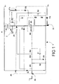
- Figure 1 is a schematic of a circuit in which a power MOSFET is used in a smart solid state relay that can be switched off before arcing can occur as an electrical connector is unmated or mated.
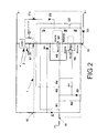
- Figure 2 is a schematic similar to Figure 1 in which two power MOSFET's are paralleled in the smart solid state relay.
- Figure 3 is a view showing the relative position of electrical contacts in an electrical connector in a fully mated configuration.
- Figure 4 is a view of the connector of Figure 3 during initial unmating of connector halves, showing the manner in which a shunt is disengaged before terminals carrying the electrical load are disconnected.
- Figure 5 is a view of the connector configuration of Figures 3 and 4, in which male and female load carrying terminals are in a position where arcing might occur if the relay had not previously opened this circuit as a result of disconnection of the shunt.
- Figure 6 is a view showing male and female terminal unmated, but with the shunt engaging the disengaged male terminal.
- Figures 7A and 7B are views of male and female terminals in an alternative embodiment of this invention in which a short terminal is disconnected before longer load terminals to allow sufficient time for the smart solid relay to switch off.
- Figure 7A shows the connector in which both long and short pins are mated and
- Figure 7B shows that the short pin is unmated before the long or load pin.
- FIG 8 is a view showing another embodiment of the solid state relay in accordance with this invention.
- This embodiment of the relay uses quick connect terminals of the type conforming to ISO 7588-2.
- Figure 9 is an exploded view of the solid state relay, also shown in Figure 8, showing two power MOSFET's used in this relay.
- Figure 10 is a schematic of an embodiment of a solid state relay in accordance with this invention that can be substituted for a conventional electromechanical relay.
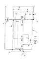
- Figure 11 is a schematic of yet another embodiment of a solid state relay in accordance with this invention.
- the embodiments of both Figures 10 and 11 are suitable for use in applications other than the prevention of arcing as an electrical connector is unmated or mated.
- Figure 12 is a view of a pin configuration for a standard mini relay that conforms to ISO 7588-2.
- Figure 13 is a view of a pin configuration for a standard mini relay that conforms to SAE J1744.
- Figure 14 is a schematic of a standard Form A relay.
- Figure 15 is a schematic of a standard relay having two switched contacts at the same voltage potential.
- the preferred embodiments of the solid state relays in accordance with this invention are intended substantially to conform to conventional standards for electromechanical relays, such as ISO 7588-2 or SAE J1744. Although these specific standards are discussed with reference to the representative embodiments of the invention, it should be understood that the elements of this inventions could be adapted to other standard or custom relay configurations. Some preferred embodiments are therefore suitable for replacement of standard electromechanical relays, without introducing current leakage common to devices employing power MOSFET's as the primary switching devices. Other preferred embodiments can be used in other applications, such as to prevent arcing when an electrical connector is mated or unmated, but these other embodiments still conform in many ways to these standards.
- the pin configurations for those relays that are used to prevent arcing still basically conform to standard pin configurations so that minimal changes to other components of wiring systems need be made.
- the standard pin designations, 30, 85, 86, 87 and 87a are used for each embodiment.
- the location of these pins are also shown in schematics of the relay circuits.
- Each of the embodiments of solid state relay has been identified as solid state relay 1, even though various embodiments may differ in detail. Certain embodiments of this relay include components that could be added as separate components to circuits in which those embodiments might be employed.
- the first embodiment of solid state relay 1 shown in Figure 1 is OFF (Q1 not conducting) with its circuitry floating, with respect to ground, until it is commanded ON by an Active Low signal at the input terminal.
- the circuitry is allowed to float to eliminate leakage current flowing from B+ to ground when the relay 1 is powered but is commanded OFF. Leakage can be a significant problem in automotive applications in which other solid state relays might be used to switch conventional loads. Even small leakage currents can significantly drain a battery when a large number of solid state relays are used in an automobile or motor vehicle.
- the solid state relay 1 shown in Figure 1 employs a conventional power MOSFET.
- an IRF 4905 MOSFET manufactured by International Rectifier is employed.
- This particular power MOSFET is relatively simple and relatively inexpensive and does not include some of the additional features of other power MOSFETs that are not required for this solid state relay application.
- the source of this power MOSFET is at a higher potential than the drain when the power MOSFET is OFF. As shown in Figure 1, the source is connected to the positive battery voltage through an intervening diode D3.
- the power MOSFET drain is connected through a connector 2 to a load, which is in turn connected to the relatively negative battery voltage. Details of this connector 2 will be subsequently discussed in greater detail.
- the load depicted in Figure 1 is representative of any one of a number of conventional loads, including inductive loads, which can be switched with this relay.
- the power MOSFET gate is connected to conventional control circuitry that need not be shown or discussed in detail. It is only necessary that this control circuitry be capable of inputting an Active Low signal to the power MOSFET, and in turn the solid state relay, is to be commanded ON.
- the solid state relay 1 When the solid state relay 1 is commanded ON, the power MOSFET Q1 turns on and begins conducting, thus providing power to the load.
- the Active Low input signal could be generated as a result of a manual command to energize a particular load, such as lights or a heater fan, or the Active Low input signal could result automatically because of a change in state of some monitored variable.
- a bipolar PNP transistor Q2 is also part of circuitry of this solid state relay.
- the emitter of transistor Q2 is connected to the positive battery voltage through diode D3.
- the collector of transistor Q2 is connected to the gate of the power MOSFET at the junction of resistors R3 and R4.
- the base of transistor Q2 is connected to the emitter through a resistor R8.
- the transistor base is also connected to the relay contact terminal 86 through resistors R9 and R7.
- the PNP transistor base is also connected to at least one pin or contact in the connector 2 through intervening resistor R9 and diode D2.
- the purpose of the PNP transistor Q2 is to monitor or sense the voltage drop across the source and drain of the power MOSFET Q1 and a shunt or short pin in the connector.
- the solid state relay 1 When the solid state relay 1 is commanded ON, with the power MOSFET conducting, the drain/source resistance Rds (on) and the current will result in a voltage drop across source/drain junction of power MOSFET Q1 that is proportional to the current flowing through the power MOSFET Q1.
- the PNP transistor Q2 turns ON, shutting off the MOSFET Q1.
- the diode D2 and resistors R8, R9 and R7 provide the capability of biasing the Emitter/Base junction of the PNP transistor to shut off the power MOSFET Q1 at varying current ranges.
- the Emitter/Base junction can be biased between 0.1V and 0.6V.
- Zener diode Z1 is connected between the positive and negative battery voltages to provide over voltage protection for the battery. For a 14 volt system, a diode Z1 will typically be selected to protect the battery from load dump transients which would exceed a predetermined value, such as 30 volts. For a 42 volt system, a diode Z1 would be selected to protect the battery from 68 volts. Diode D3 is connected at the positive battery voltage to protect circuitry connected to the battery from reverse battery connection. Diode D1 is connected between the negative battery voltage and a point between the load and the drain of power MOSFET Q1.
- Diode D1 is a free wheeling diode that protects the relay 1 from transients generated by disconnection from inductive loads.
- the RC circuit of R4 and C1 provides immunity from transients, such as inrush current from lamp loads, prematurely shutting off power MOSFET Q1.
- Zener diode Z2 limits the gate voltage of the power MOSFET Q1 and provides a constant voltage for operation of PNP transistor Q2. Pull up resistor R2, between the gate drive circuit and positive voltage potential prevents inadvertent triggering of the relay 1.
- the solid state relay 1 is used in conjunction with a connector 2 in a configuration that will prevent arcing when the electrical connector is disconnected from the load.
- arcing has not been regarded as a problem in many applications, such as 14 Volt automotive electrical systems, a 42 volt electrical system could result in arcing problems, especially when an electrical connector is disconnected under load.
- At least one load pin is included in the connector for conducting current through the power MOSFET Q1 and the load.
- the connector 2 also includes a short pin or a shunt. Either the short pin or the shunt would be disconnected prior to disconnection of the load pin. As shown in Figure 1, either the shunt or the short pin is connected to the drain of the power MOSFET Q1.
- the short pin or shunt is connected indirectly to the base of the transistor Q2, disconnection of the short pin or shunt, or the drain of the power MOSFET Q1, will cause the PNP transistor Q2 to switch ON. Since the transistor Q2 is connected between the positive battery voltage and the gate of the power MOSFET, the gate will be in a high state when the transistor Q2 is ON, conducting current from the positive battery voltage. Since the power MOSFET Q1 is off when the gate is in a high state, the power MOSFET Q1 will revert to the OFF or nonconducting state when the transistor Q2 is ON and, one event that will turn the transistor Q2 On, is the disconnection of the short pin or shunt in connector 2.
- This solid state relay 1 is sufficiently fast that a short pin that is approximately 5 mm (0.200 inches) shorter than a load pin will provide adequate time for the relay 1 to switch from an ON to and OFF state before arcing will occur as the longer load pin is disconnected in the connector 2.
- FIG. 2 shows a solid state relay 1 in which two power MOSFET's Q1 and Q3 are connected in parallel between the positive battery voltage and the load.
- Resistor R6, having the same value as Resistor R5 is connected to the gate of power MOSFET Q3 in the same manner as Resistor R5 is connected to the gate of power MOSFET Q1.
- the same input will be applied to the two gates of the two power MOSFET's Q1 and Q3. Additional power MOSFET devices can be paralleled in the same manner.
- This connector 2 has two mating connector halves 10, 20, the first of which includes at least male terminal or load pin 12.
- This male terminal or load pin 12 carries the current between the drain of the power MOSFET Q1 and the load 4, and is terminated to the drain, or to a wire or conductor leading to the drain.
- a mating female terminal 22 in a second connector half 20 is connected to the load 4, either directly or indirectly by means of an electrical conductor.
- the first connector half 10 includes a shunt 16, that protrudes beyond the male terminal 12 and the housing 14 of the first connector half 10. The shunt 16 must be connected to relay 1, terminal 87a and will be connected to the base of the PNP transistor Q2, through diode D2 and resistor R9, when this first connector half 10 is fully mated with the second connector half 20.
- the shunt 16 comprises a deflectable cantilever spring that will also engage the female terminal 22 in the second connector half at a contact point 18 when the two connector halves 10, 20 are fully mated as shown in Figure 3.
- the shunt 16 When the shunt 16 is connected to the female terminal 22, the shunt 16 will also be connected to the male terminal 12 and consequently to the drain of power MOSFET Q1.
- the housing 24 of the second connector half includes a protruding section 26 with a ramping surface 28 that is opposed to the cantilever beam section of the shunt 16. As the second connector half 20 is unmated from the first connector half 10, a portion of the shunt 16 adjacent the contact point 18 will engage this ramping surface 28.
- FIG. 7A and 7B An alternative connector configuration that can be used with this solid state relay 1 is illustrated by the mating terminals shown in Figures 7A and 7B.
- This configuration employs two male terminals which can be in the form of blades or pins or other conventional configurations.
- a longer load pin 32 is connected to relay terminal 87.
- a shorter pin 34 is connected to the relay terminal 87a.
- the relay terminal 87a is connected to the relay terminal 87.
- the load male terminal or terminals 32 is longer than the separate short male terminal 34 that is connected through diode D2 to the base of the monitoring transistor Q2.
- FIGs 8 and 9 show a relay apparatus incorporating the elements of this invention in a standard relay configuration.
- Relay 1 includes pins 30, 85, 86, 87, and 87a in a standard pin configuration conforming to ISO 7588-2. Other standard pin configurations are also possible.
- Relay 1 also includes a printed circuit board 40 on which the other circuit components can be mounted. This configuration also provides the capability of biasing the Emitter/Base junction of the PNP transistor Q2 between 0.1V and 0.6V. by replacing resistor R9 with a resistor of an appropriate value. As shown in Figure 9, this relay includes two power MOSFET's Q1 and Q3, so this embodiment will conform to the circuit shown in Figure 2.
- Figures 1-7 demonstrate the use of a solid state relay in accordance with this invention in which the relay is used to prevent arcing when an electrical connector is mated or unmated.
- Solid state relays used to prevent arcing can be assembled as shown in Figures 8 and 9.
- Solid state relays of this type can also be used for other applications.
- the solid state relay shown in the schematic of Figure 10, can be substituted for a conventional electromechanical relay having the same rating. Pin 30 would be connected to the positive potential, pin 87 would be connected to the load and pin 86 would be connected to a disconnectable ground, such as an external switch.
- a standard electromechanical relay used in the same circuit would have the same electrical connections.
- Figure 11 shows a version of a solid state relay in which the Zener Diode Z1 and the freewheeling diode D1 are incorporated in the relay in much the same manner as the schematics of Figures 1 and 2.
- the embodiment of Figure 11 would, however, require a ground connection 85 that would not normally be available for standard electromechanical relays of this type.
- the standard pin configuration for an ISO 7588-2 mini relay is shown in Figure 12. Primary dimensions are shown in inches with equivalent dimensions in mm. also shown in the view.
- Each of the versions of the solid state relay 1 depicted herein can be implemented with the pin configuration shown in Figure 12. These versions of the solid state relay 1 can also be implement in the pin configuration for a standard mini SAE J1744 relay as shown in Figure 13. These are the two standard relay configurations used for automotive electrical systems, and the smart solid state relay 1 of this invention is basically compatible with each standard relay.
- Figure 14 is a simple schematic for a standard Form A relay.
- a Form A relay has one switchable output and the smart solid state relay 1 of this invention has the functionality of a standard Form A relay.
- Figure 15 is a simple schematic for a relay having a switched output pin 87 and a sense pin 87a. It is this pin configuration with which the smart solid state relay 1 can be used to prevent arcing, as shown in Figures 1-7.
- the relays of Figures 1 and 2 will provide the means to shut off current to the load pins that remain connected to relay output 87 after the short pin or shunt connected to relay sense pin 87a has been disconnected.
Landscapes
- Physics & Mathematics (AREA)
- Electromagnetism (AREA)
- Emergency Protection Circuit Devices (AREA)
- Relay Circuits (AREA)
- Details Of Connecting Devices For Male And Female Coupling (AREA)
- Direct Current Feeding And Distribution (AREA)
- Charge And Discharge Circuits For Batteries Or The Like (AREA)
- Protection Of Static Devices (AREA)
- Electronic Switches (AREA)
Applications Claiming Priority (2)
| Application Number | Priority Date | Filing Date | Title |
|---|---|---|---|
| US68925 | 2002-02-08 | ||
| US10/068,925 US6891705B2 (en) | 2002-02-08 | 2002-02-08 | Smart solid state relay |
Publications (3)
| Publication Number | Publication Date |
|---|---|
| EP1335471A2 true EP1335471A2 (de) | 2003-08-13 |
| EP1335471A3 EP1335471A3 (de) | 2005-06-22 |
| EP1335471B1 EP1335471B1 (de) | 2011-01-12 |
Family
ID=27610532
Family Applications (1)
| Application Number | Title | Priority Date | Filing Date |
|---|---|---|---|
| EP03250795A Expired - Lifetime EP1335471B1 (de) | 2002-02-08 | 2003-02-07 | Halbleiterrelais |
Country Status (8)
| Country | Link |
|---|---|
| US (2) | US6891705B2 (de) |
| EP (1) | EP1335471B1 (de) |
| JP (1) | JP2003258615A (de) |
| KR (1) | KR100964440B1 (de) |
| BR (1) | BR0300297A (de) |
| CA (1) | CA2418576C (de) |
| DE (1) | DE60335684D1 (de) |
| ES (1) | ES2357104T3 (de) |
Cited By (5)
| Publication number | Priority date | Publication date | Assignee | Title |
|---|---|---|---|---|
| WO2007113117A1 (de) * | 2006-04-06 | 2007-10-11 | Robert Bosch Gmbh | Steckvorrichtung zur kontaktierung der hochspannungsbaugruppe eines hybridfahrzeugs sowie hochspannungsbaugruppe eines hybridfahrzeugs |
| WO2008076160A1 (en) * | 2006-12-18 | 2008-06-26 | Caterpillar Inc. | Electrical shorting system |
| US7616421B2 (en) | 2006-12-18 | 2009-11-10 | Caterpillar Inc. | Electrical interface system |
| FR2939959A1 (fr) * | 2008-12-16 | 2010-06-18 | Eurocopter France | Commande anti-charbonnage par interruption en tension pour aeronef |
| US12153081B1 (en) | 2023-06-22 | 2024-11-26 | Turck Holding Gmbh | Device and method for monitoring a turn-off capability |
Families Citing this family (20)
| Publication number | Priority date | Publication date | Assignee | Title |
|---|---|---|---|---|
| KR100434153B1 (ko) * | 2002-04-12 | 2004-06-04 | 엘지산전 주식회사 | 하이브리드 직류 전자 접촉기 |
| JP2005532009A (ja) * | 2002-07-03 | 2005-10-20 | クント・エレクトロニック・サナイ・ヴェ・チカレット・アノニム・シルケチ | 電子スイッチングモジュール |
| US7265959B2 (en) * | 2005-01-25 | 2007-09-04 | Yazaki North America, Inc. | Solid state switch with quasi-predictive short circuit protection and thermal protection |
| US7998218B1 (en) | 2005-02-02 | 2011-08-16 | Biomet Manufacturing Corp. | Modular orthopedic implant |
| US20060238936A1 (en) * | 2005-04-25 | 2006-10-26 | Blanchard Richard A | Apparatus and method for transient blocking employing relays |
| US20060250736A1 (en) * | 2005-05-06 | 2006-11-09 | Harris Richard A | Transient blocking apparatus with electrostatic discharge protection |
| US7538454B2 (en) * | 2005-06-30 | 2009-05-26 | Honeywell International Inc. | Leakage current shunt in an electrical power distribution system utilizing solid state relays |
| US8203810B2 (en) * | 2006-04-04 | 2012-06-19 | Tyco Electronics Corporation | Solid state pre-charge module |
| JP4645524B2 (ja) * | 2006-05-24 | 2011-03-09 | パナソニック電工株式会社 | リレー |
| US7961443B2 (en) * | 2007-04-06 | 2011-06-14 | Watlow Electric Manufacturing Company | Hybrid power relay using communications link |
| US8619395B2 (en) | 2010-03-12 | 2013-12-31 | Arc Suppression Technologies, Llc | Two terminal arc suppressor |
| JP6297342B2 (ja) * | 2013-05-23 | 2018-03-20 | 株式会社ミツバ | 半導体リレー |
| US9923470B2 (en) | 2015-09-18 | 2018-03-20 | Lear Corporation | High voltage pre-charge system |
| US9857397B2 (en) | 2016-04-07 | 2018-01-02 | Sensata Technologies, Inc. | Modular packaging with elevating screw |
| CN108630129A (zh) * | 2018-06-12 | 2018-10-09 | 浩腾和润(北京)科技有限公司 | 一种集成cave投射系统 |
| CN109672433B (zh) * | 2018-11-29 | 2023-01-13 | 杭州电子科技大学 | 一种具有短路保护的igbt高压直流固态继电器电路 |
| CN109672432B (zh) * | 2018-11-29 | 2023-01-13 | 杭州电子科技大学 | 一种具有短路保护的mosfet直流固态继电器电路 |
| US10601421B1 (en) | 2019-08-30 | 2020-03-24 | Ademco Inc. | MOSFET based isolation circuit |
| US11788760B2 (en) | 2020-11-04 | 2023-10-17 | Ademco Inc. | Power stealing system for low power thermostats |
| KR102763943B1 (ko) * | 2023-12-26 | 2025-02-07 | 전성기 | 전기차량용 릴레이 회로 |
Citations (3)
| Publication number | Priority date | Publication date | Assignee | Title |
|---|---|---|---|---|
| US4346419A (en) | 1981-04-27 | 1982-08-24 | Clairol Incorporated | Detachable plug |
| US5926354A (en) | 1997-06-11 | 1999-07-20 | International Rectifier Corporation | Solid state relay and circuit breaker |
| DE19838492A1 (de) | 1998-08-25 | 2000-03-09 | Stahl R Schaltgeraete Gmbh | Explosionsgeschützte Steckverbindungsanordnung |
Family Cites Families (19)
| Publication number | Priority date | Publication date | Assignee | Title |
|---|---|---|---|---|
| US3614464A (en) * | 1969-04-22 | 1971-10-19 | Ite Imperial Corp | Arcless tap- or source-switching apparatus using series-connected semiconductors |
| US4438472A (en) * | 1982-08-09 | 1984-03-20 | Ibm Corporation | Active arc suppression for switching of direct current circuits |
| US4628392A (en) * | 1983-12-20 | 1986-12-09 | Biw Cable Systems, Inc. | Explosion proof electrical connector system with quick power disconnect |
| US4700256A (en) | 1984-05-16 | 1987-10-13 | General Electric Company | Solid state current limiting circuit interrupter |
| US4631621A (en) * | 1985-07-11 | 1986-12-23 | General Electric Company | Gate turn-off control circuit for a solid state circuit interrupter |
| JPS62223931A (ja) | 1986-03-25 | 1987-10-01 | 松下電工株式会社 | 電磁継電器 |
| US4700258A (en) * | 1986-07-21 | 1987-10-13 | Colt Industries Inc. | Lightning arrester system for underground loop distribution circuit |
| US4959746A (en) * | 1987-01-30 | 1990-09-25 | Electronic Specialty Corporation | Relay contact protective circuit |
| US4992904A (en) * | 1989-11-14 | 1991-02-12 | Sundstrand Corporation | Hybrid contactor for DC airframe power supply |
| US5164872A (en) * | 1991-06-17 | 1992-11-17 | General Electric Company | Load circuit commutation circuit |
| US5536980A (en) * | 1992-11-19 | 1996-07-16 | Texas Instruments Incorporated | High voltage, high current switching apparatus |
| US5497285A (en) * | 1993-09-14 | 1996-03-05 | International Rectifier Corporation | Power MOSFET with overcurrent and over-temperature protection |
| US5463252A (en) * | 1993-10-01 | 1995-10-31 | Westinghouse Electric Corp. | Modular solid state relay |
| US5703743A (en) * | 1996-04-29 | 1997-12-30 | Schweitzer Engineering Laboratories, Inc. | Two terminal active arc suppressor |
| US5633540A (en) * | 1996-06-25 | 1997-05-27 | Lutron Electronics Co., Inc. | Surge-resistant relay switching circuit |
| US5881251A (en) * | 1996-10-10 | 1999-03-09 | Bay Networks, Inc. | Hot swap control circuit |
| US6057998A (en) * | 1996-12-25 | 2000-05-02 | Hitachi, Ltd. | Insulated gate type semiconductor apparatus with a control circuit |
| US5933304A (en) * | 1998-04-28 | 1999-08-03 | Carlingswitch, Inc. | Apparatus and method of interrupting current for reductions in arcing of the switch contacts |
| JP3903713B2 (ja) | 2000-12-13 | 2007-04-11 | アンデン株式会社 | 電磁継電器 |
-
2002
- 2002-02-08 US US10/068,925 patent/US6891705B2/en not_active Expired - Fee Related
-
2003
- 2003-02-06 CA CA002418576A patent/CA2418576C/en not_active Expired - Fee Related
- 2003-02-07 BR BR0300297-7A patent/BR0300297A/pt not_active IP Right Cessation
- 2003-02-07 DE DE60335684T patent/DE60335684D1/de not_active Expired - Lifetime
- 2003-02-07 ES ES03250795T patent/ES2357104T3/es not_active Expired - Lifetime
- 2003-02-07 EP EP03250795A patent/EP1335471B1/de not_active Expired - Lifetime
- 2003-02-08 KR KR1020030008013A patent/KR100964440B1/ko not_active Expired - Fee Related
- 2003-02-10 JP JP2003032461A patent/JP2003258615A/ja active Pending
-
2004
- 2004-06-08 US US10/864,243 patent/US7271990B2/en not_active Expired - Lifetime
Patent Citations (3)
| Publication number | Priority date | Publication date | Assignee | Title |
|---|---|---|---|---|
| US4346419A (en) | 1981-04-27 | 1982-08-24 | Clairol Incorporated | Detachable plug |
| US5926354A (en) | 1997-06-11 | 1999-07-20 | International Rectifier Corporation | Solid state relay and circuit breaker |
| DE19838492A1 (de) | 1998-08-25 | 2000-03-09 | Stahl R Schaltgeraete Gmbh | Explosionsgeschützte Steckverbindungsanordnung |
Cited By (8)
| Publication number | Priority date | Publication date | Assignee | Title |
|---|---|---|---|---|
| WO2007113117A1 (de) * | 2006-04-06 | 2007-10-11 | Robert Bosch Gmbh | Steckvorrichtung zur kontaktierung der hochspannungsbaugruppe eines hybridfahrzeugs sowie hochspannungsbaugruppe eines hybridfahrzeugs |
| WO2008076160A1 (en) * | 2006-12-18 | 2008-06-26 | Caterpillar Inc. | Electrical shorting system |
| US7616421B2 (en) | 2006-12-18 | 2009-11-10 | Caterpillar Inc. | Electrical interface system |
| US7789685B2 (en) | 2006-12-18 | 2010-09-07 | Caterpillar Inc | Electrical shorting system |
| FR2939959A1 (fr) * | 2008-12-16 | 2010-06-18 | Eurocopter France | Commande anti-charbonnage par interruption en tension pour aeronef |
| EP2200181A1 (de) * | 2008-12-16 | 2010-06-23 | Eurocopter | Steuereinrichtung zur Spannungsunterbrechung für ein Luftfahrzeug welche Kontaktbrand verhindert |
| US12153081B1 (en) | 2023-06-22 | 2024-11-26 | Turck Holding Gmbh | Device and method for monitoring a turn-off capability |
| EP4481411A1 (de) | 2023-06-22 | 2024-12-25 | Turck Holding GmbH | Vorrichtung und verfahren zum überwachen einer abschaltfähigkeit |
Also Published As
| Publication number | Publication date |
|---|---|
| JP2003258615A (ja) | 2003-09-12 |
| BR0300297A (pt) | 2004-08-03 |
| ES2357104T3 (es) | 2011-04-18 |
| US7271990B2 (en) | 2007-09-18 |
| DE60335684D1 (de) | 2011-02-24 |
| CA2418576A1 (en) | 2003-08-08 |
| KR100964440B1 (ko) | 2010-06-16 |
| US20040223278A1 (en) | 2004-11-11 |
| CA2418576C (en) | 2008-05-06 |
| US20030151860A1 (en) | 2003-08-14 |
| US6891705B2 (en) | 2005-05-10 |
| EP1335471A3 (de) | 2005-06-22 |
| EP1335471B1 (de) | 2011-01-12 |
| KR20030067594A (ko) | 2003-08-14 |
Similar Documents
| Publication | Publication Date | Title |
|---|---|---|
| US6891705B2 (en) | Smart solid state relay | |
| US11186191B2 (en) | Charging device for electric vehicle | |
| CN207588156U (zh) | 具有电路保护装置的电力电缆组件 | |
| CN1262057C (zh) | 电子开关 | |
| US6172892B1 (en) | Method for using battery charger adapter for military vehicles | |
| KR100829684B1 (ko) | 전기 커넥터들 사이의 아킹을 최소화시키기 위한 장치 및방법 | |
| CN107112747B (zh) | 限流电路、直流电力供给连接器和直流电源装置 | |
| EP1445839A1 (de) | System und verfahren zum verhindern elektrischer bogen in verbindern, die stromladungen liefern, und verbinder dafür | |
| EP2677616B1 (de) | Schnittstelleneinheit mit Überstrom- und Überspannungsschutzvorrichtung | |
| CN104716520A (zh) | 电源线 | |
| CN103209853A (zh) | 用于从连接装置分离蓄电池的供电装置和方法以及机动车 | |
| JP2003141973A (ja) | 電源遮断時における保護装置 | |
| CN105556791A (zh) | 中继连接器和电池组 | |
| US5099187A (en) | Power connect safety and connection interlock | |
| US6678183B2 (en) | DC power conditioning system | |
| US20240105411A1 (en) | Status detection circuit and remotely operable switch | |
| CA2614973C (en) | Smart solid state relay | |
| CN220291869U (zh) | 一种驱动电路、电池管理系统及车辆 | |
| CN109074979A (zh) | 电弧抑制连接器 | |
| CN208445334U (zh) | 一种低压供电系统 | |
| KR20050027534A (ko) | 자동차의 과전류 보호용 폴리스위치 | |
| JP2001307834A (ja) | コネクタ及び配線構造 | |
| KR20040020114A (ko) | 서지 전류 저감을 위한 커넥터 | |
| KR19980055535A (ko) | 초기 과전류 방지 스위치 |
Legal Events
| Date | Code | Title | Description |
|---|---|---|---|
| PUAI | Public reference made under article 153(3) epc to a published international application that has entered the european phase |
Free format text: ORIGINAL CODE: 0009012 |
|
| AK | Designated contracting states |
Designated state(s): AT BE BG CH CY CZ DE DK EE ES FI FR GB GR HU IE IT LI LU MC NL PT SE SI SK TR |
|
| AX | Request for extension of the european patent |
Extension state: AL LT LV MK RO |
|
| PUAL | Search report despatched |
Free format text: ORIGINAL CODE: 0009013 |
|
| AK | Designated contracting states |
Kind code of ref document: A3 Designated state(s): AT BE BG CH CY CZ DE DK EE ES FI FR GB GR HU IE IT LI LU MC NL PT SE SI SK TR |
|
| AX | Request for extension of the european patent |
Extension state: AL LT LV MK RO |
|
| 17P | Request for examination filed |
Effective date: 20051219 |
|
| AKX | Designation fees paid |
Designated state(s): DE ES FR GB IT |
|
| 17Q | First examination report despatched |
Effective date: 20080930 |
|
| GRAP | Despatch of communication of intention to grant a patent |
Free format text: ORIGINAL CODE: EPIDOSNIGR1 |
|
| GRAS | Grant fee paid |
Free format text: ORIGINAL CODE: EPIDOSNIGR3 |
|
| GRAA | (expected) grant |
Free format text: ORIGINAL CODE: 0009210 |
|
| AK | Designated contracting states |
Kind code of ref document: B1 Designated state(s): DE ES FR GB IT |
|
| REG | Reference to a national code |
Ref country code: GB Ref legal event code: FG4D |
|
| REF | Corresponds to: |
Ref document number: 60335684 Country of ref document: DE Date of ref document: 20110224 Kind code of ref document: P |
|
| REG | Reference to a national code |
Ref country code: DE Ref legal event code: R096 Ref document number: 60335684 Country of ref document: DE Effective date: 20110224 |
|
| REG | Reference to a national code |
Ref country code: ES Ref legal event code: FG2A Ref document number: 2357104 Country of ref document: ES Kind code of ref document: T3 Effective date: 20110418 |
|
| PLBE | No opposition filed within time limit |
Free format text: ORIGINAL CODE: 0009261 |
|
| STAA | Information on the status of an ep patent application or granted ep patent |
Free format text: STATUS: NO OPPOSITION FILED WITHIN TIME LIMIT |
|
| 26N | No opposition filed |
Effective date: 20111013 |
|
| REG | Reference to a national code |
Ref country code: DE Ref legal event code: R097 Ref document number: 60335684 Country of ref document: DE Effective date: 20111013 |
|
| PGFP | Annual fee paid to national office [announced via postgrant information from national office to epo] |
Ref country code: IT Payment date: 20120223 Year of fee payment: 10 |
|
| PGFP | Annual fee paid to national office [announced via postgrant information from national office to epo] |
Ref country code: ES Payment date: 20130226 Year of fee payment: 11 Ref country code: DE Payment date: 20130227 Year of fee payment: 11 Ref country code: FR Payment date: 20130311 Year of fee payment: 11 Ref country code: GB Payment date: 20130227 Year of fee payment: 11 |
|
| REG | Reference to a national code |
Ref country code: DE Ref legal event code: R119 Ref document number: 60335684 Country of ref document: DE |
|
| GBPC | Gb: european patent ceased through non-payment of renewal fee |
Effective date: 20140207 |
|
| REG | Reference to a national code |
Ref country code: FR Ref legal event code: ST Effective date: 20141031 |
|
| REG | Reference to a national code |
Ref country code: DE Ref legal event code: R119 Ref document number: 60335684 Country of ref document: DE Effective date: 20140902 |
|
| PG25 | Lapsed in a contracting state [announced via postgrant information from national office to epo] |
Ref country code: GB Free format text: LAPSE BECAUSE OF NON-PAYMENT OF DUE FEES Effective date: 20140207 Ref country code: DE Free format text: LAPSE BECAUSE OF NON-PAYMENT OF DUE FEES Effective date: 20140902 Ref country code: FR Free format text: LAPSE BECAUSE OF NON-PAYMENT OF DUE FEES Effective date: 20140228 |
|
| REG | Reference to a national code |
Ref country code: ES Ref legal event code: FD2A Effective date: 20150504 |
|
| PG25 | Lapsed in a contracting state [announced via postgrant information from national office to epo] |
Ref country code: ES Free format text: LAPSE BECAUSE OF NON-PAYMENT OF DUE FEES Effective date: 20140208 |
|
| PG25 | Lapsed in a contracting state [announced via postgrant information from national office to epo] |
Ref country code: IT Free format text: LAPSE BECAUSE OF NON-PAYMENT OF DUE FEES Effective date: 20140207 |