EP1335519A2 - Procédé pour générer une séquence d'impulsions de signal avec une fréquence de base prédéterminée - Google Patents
Procédé pour générer une séquence d'impulsions de signal avec une fréquence de base prédéterminée Download PDFInfo
- Publication number
- EP1335519A2 EP1335519A2 EP03000570A EP03000570A EP1335519A2 EP 1335519 A2 EP1335519 A2 EP 1335519A2 EP 03000570 A EP03000570 A EP 03000570A EP 03000570 A EP03000570 A EP 03000570A EP 1335519 A2 EP1335519 A2 EP 1335519A2
- Authority
- EP
- European Patent Office
- Prior art keywords
- frequency
- filter
- signal
- fundamental frequency
- clock signal
- Prior art date
- Legal status (The legal status is an assumption and is not a legal conclusion. Google has not performed a legal analysis and makes no representation as to the accuracy of the status listed.)
- Withdrawn
Links
Images

Classifications
-
- H—ELECTRICITY
- H04—ELECTRIC COMMUNICATION TECHNIQUE
- H04L—TRANSMISSION OF DIGITAL INFORMATION, e.g. TELEGRAPHIC COMMUNICATION
- H04L7/00—Arrangements for synchronising receiver with transmitter
- H04L7/02—Speed or phase control by the received code signals, the signals containing no special synchronisation information
- H04L7/027—Speed or phase control by the received code signals, the signals containing no special synchronisation information extracting the synchronising or clock signal from the received signal spectrum, e.g. by using a resonant or bandpass circuit
-
- H—ELECTRICITY
- H04—ELECTRIC COMMUNICATION TECHNIQUE
- H04L—TRANSMISSION OF DIGITAL INFORMATION, e.g. TELEGRAPHIC COMMUNICATION
- H04L7/00—Arrangements for synchronising receiver with transmitter
- H04L7/02—Speed or phase control by the received code signals, the signals containing no special synchronisation information
- H04L7/033—Speed or phase control by the received code signals, the signals containing no special synchronisation information using the transitions of the received signal to control the phase of the synchronising-signal-generating means, e.g. using a phase-locked loop
Definitions
- the invention relates to a method for generating a signal pulse sequence with a predetermined stable fundamental frequency, i.e. the recovery of a clock signal (clock recovery) according to the preamble of claim 1.
- the object of the invention is to provide a simple method with which a frequency stable clock signal from one noisy clock signal can be recovered.
- the digital filter comprises a bandpass filter that locks at zero frequency and half the sampling frequency, and a zero crossing detector that is present at each zero crossing generates a clock signal pulse.
- the band filter is a FIR filter and an IIR filter that is in series are switched, the natural frequency of the IIR filter is equal to the fundamental frequency.
- the fundamental frequency is determined by a PLL control loop multiplied after the digital filter.
- the multiplied fundamental frequency can PLL control loop as the sampling frequency of the bandpass filter and the Zero crossing detector can be used.
- An advantage of the invention is that there is no complex and precise PLL control is required.
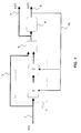
- Fig. 1 shows a filter structure with which the invention Procedure can be carried out.
- FIG. 2 shows the transmission curve of the filter according to FIG. 1.
- FIG. 3 shows a timing diagram for explaining the generation the frequency-stable signal pulses from an input pulse sequence, which is not frequency stable.
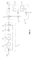
- FIG. 4 shows an embodiment of the band filter from FIG. 1.
- Fig. 1 is a filter structure for generating a signal pulse train shown with a predetermined stable fundamental frequency with which the method according to the invention is carried out leaves.
- the filter structure is connected via an input 1 with a Sequence of signal pulses x (n) supplied, the frequency fluctuates and not directly for clocking time-critical Operations used in a circuit (not shown) can be.
- the frequency fluctuations of the input pulses can be understood such that the input pulses have spectral components in addition to their desired basic frequency f 0 , the frequency of which is above the basic frequency and in particular is at least a predetermined multiple of the basic frequency f 0 .
- the spectral component of the input pulses with f 0 or a multiple thereof is used regardless of its amplitude in order to excite a system to (resonance) vibrations.
- the vibrations of the system then serve as a reference for the generation of the desired frequency-stable clock signal.
- the zero crossing of the (resonance) oscillation amplitude is recorded in a preferred embodiment of the invention.
- a corresponding blocking filter is provided, by means of which all undesired frequency components are suppressed.
- the sequence of signal pulses x (n) is fed to a digital filter 2, the pass band of which is around the fundamental frequency f 0 and which blocks by a predetermined half sampling frequency f a / 2.
- the filter in the pass band, ie when energized, the filter is designed in such a way that it outputs a signed output signal.
- a filter is the bandpass filter 4, which is part of the digital filter 2. If the incoming signal component therefore has a frequency that differs from the desired fundamental frequency f 0 , the bandpass filter 4 and thus the digital filter 2 are blocked, so that no clock signal is present at the following circuit.
- the bandpass filter 4 is excited to oscillate by this frequency component, the oscillation frequency being the desired natural frequency.
- the output signal of the band filter 4 is in a zero point detector 5 coupled in, each time the sign changes Output signal of the band filter 4 generates a clock signal pulse.
- the functioning and the technical implementation of a such zero point detector 5 is known to the person skilled in the art and is therefore not explained further here. Otherwise, you can other elements are used, which are used in the passage of the Output signal from the bandpass filter 4 by a certain one Value (maximum or minimum) generate a clock pulse.
- the clock pulses y (n) generated by the zero point detector 5 have the frequency f 0 , which is the resonance frequency of the bandpass filter 4 and is equal to the desired frequency.
- the frequency-stable clock pulses y (n) can now continue to work be or be used directly. In the second case via an output 7 into the (not shown) subsequent circuit fed, otherwise they will implemented with a PLL control loop 8 to a higher frequency and only then via an output 9 into the (not shown) subsequent circuit fed.
- the multiplied frequency according to the PLL control loop 8 can at the same time as a control clock for the components described above of digital filter 2 can be used to oversampling (oversampling) the input signal of these components to control. It is therefore in the embodiment shown 1 looped back via a feedback line 10 and is due to the bandpass filter 4 and the zero point detector 5 in the digital filter 2.
- a multiplexer 6 and a bypass line 3 are provided in the embodiment shown, which means at the beginning of the clock signal recovery, ie immediately after switching on the Filter construction of the PLL control circuit 8 is first started up with the frequency-unstable clock, and after the end of the transient process, the input of the PLL control circuit 8 is switched to the frequency-stable clock signal with the multiplexer 6.
- Fig. 3 the sequence of input pulses A is shown. These have approximately the desired frequency f 0 , but are subject to frequency fluctuations, which are indicated by the deviations of their flanks from the "exact" vertical lines.
- the deviation of the actual frequency of the input pulses A from the target frequency means that the spectral components in the input pulses A with the desired frequency f 0 have a different amplitude.
- the bandpass filter 4 oscillates at its resonance frequency f 0 , excited by the spectral components with f 0 in the input pulses.
- the oscillation amplitude of the bandpass filter is designated B in FIG. 3. It fluctuates depending on the "correspondence" of the frequency of the input pulses A with the resonance frequency of the bandpass filter 4.
- the bandpass filter 4 shows a possible embodiment of the bandpass filter 4.
- the bandpass filter 4 is composed of an FIR filter 11 and an IIR filter 12, which are connected in series.
- the natural frequency of the IIR filter 12 is equal to the desired fundamental frequency f 0 .
- the structure of the FIR filter 11 and the IIR filter 12 from delay elements 13, adders 14 and multipliers 15 is known to the person skilled in the art and will not be explained further here.
- the multipliers 15 each multiply with their own value, which is not shown in the figure, but which generally differs from that of other multipliers 15 and can also be negative, if appropriate.
- a digital IIR filter 12 is used to generate an oscillation with the desired frequency f 0 . This is because each time the clock signal C is switched over, the IIR filter 12 is reinitialized. This reinitialization always takes place, regardless of whether there is a change in the amplitude of the signal B or not. With each of these reinitializations, the state of the IIR filter 12 is changed, so that the IIR filter is always in a steady state for the signal component with the frequency f 0 .
- Another feature of the invention is that the work cycle, which the filter itself needs to be able to work, is provided by the PLL control loop 8, which in turn receives its frequency-stable clock signal from the filter. Filter 2 is only switched on when the PLL control loop 8 has settled. Before the clock signal on Filter 2 passed.
- the delay elements are preferably registers with one 8 bits wide.
Landscapes
- Engineering & Computer Science (AREA)
- Computer Networks & Wireless Communication (AREA)
- Signal Processing (AREA)
- Stabilization Of Oscillater, Synchronisation, Frequency Synthesizers (AREA)
- Manipulation Of Pulses (AREA)
Applications Claiming Priority (2)
| Application Number | Priority Date | Filing Date | Title |
|---|---|---|---|
| DE10203892 | 2002-01-31 | ||
| DE10203892A DE10203892B4 (de) | 2002-01-31 | 2002-01-31 | Verfahren zum Erzeugen einer Signalpulsfolge mit einer vorgegebenen stabilen Grundfrequenz |
Publications (2)
| Publication Number | Publication Date |
|---|---|
| EP1335519A2 true EP1335519A2 (fr) | 2003-08-13 |
| EP1335519A3 EP1335519A3 (fr) | 2004-08-04 |
Family
ID=27588192
Family Applications (1)
| Application Number | Title | Priority Date | Filing Date |
|---|---|---|---|
| EP03000570A Withdrawn EP1335519A3 (fr) | 2002-01-31 | 2003-01-13 | Procédé pour générer une séquence d'impulsions de signal avec une fréquence de base prédéterminée |
Country Status (3)
| Country | Link |
|---|---|
| US (1) | US7085951B2 (fr) |
| EP (1) | EP1335519A3 (fr) |
| DE (1) | DE10203892B4 (fr) |
Families Citing this family (2)
| Publication number | Priority date | Publication date | Assignee | Title |
|---|---|---|---|---|
| US7508886B2 (en) | 2005-03-29 | 2009-03-24 | Lockheed Martin Corporation | System for generating a digital signal |
| US7848220B2 (en) | 2005-03-29 | 2010-12-07 | Lockheed Martin Corporation | System for modeling digital pulses having specific FMOP properties |
Family Cites Families (13)
| Publication number | Priority date | Publication date | Assignee | Title |
|---|---|---|---|---|
| DE6942183U (de) | 1969-10-29 | 1970-03-12 | Hellmut Hugendubel | Schirm |
| US4472785A (en) * | 1980-10-13 | 1984-09-18 | Victor Company Of Japan, Ltd. | Sampling frequency converter |
| US5136267A (en) * | 1990-12-26 | 1992-08-04 | Audio Precision, Inc. | Tunable bandpass filter system and filtering method |
| EP0610638A1 (fr) | 1993-01-13 | 1994-08-17 | A.M.C. ADVANCED MEDICAL CONCEPTS Ltd. | Un ensemble pour incontinent |
| US5425060A (en) * | 1993-01-25 | 1995-06-13 | Harris Corporation | Mechanism for reducing timing jitter in clock recovery scheme for blind acquisition of full duplex signals |
| US5388127A (en) * | 1993-02-09 | 1995-02-07 | Hitachi America, Ltd. | Digital timing recovery circuit |
| US5584062A (en) * | 1994-01-24 | 1996-12-10 | Motorola, Inc. | Method and apparatus for compensating phase locked receivers |
| US5945889A (en) * | 1997-08-13 | 1999-08-31 | Texas Instruments Incorporated | Method and apparatus for tuning high Q bandpass filters using pulse excitation |
| US6091205A (en) * | 1997-10-02 | 2000-07-18 | Lutron Electronics Co., Inc. | Phase controlled dimming system with active filter for preventing flickering and undesired intensity changes |
| KR100305646B1 (ko) * | 1998-05-29 | 2001-11-30 | 박종섭 | 클럭보정회로 |
| FR2783059B1 (fr) * | 1998-09-08 | 2002-01-18 | Thomson Csf | Camera cinevideo |
| US6236691B1 (en) * | 1999-03-16 | 2001-05-22 | International Automated Systems, Inc. | Signal demodulation method and apparatus |
| US6680644B2 (en) * | 2001-09-26 | 2004-01-20 | Siemens Information & Communication Networks, Inc. | Digital interpolation window filter for phase-locked loop operation with randomly jittered reference clock |
-
2002
- 2002-01-31 DE DE10203892A patent/DE10203892B4/de not_active Expired - Lifetime
-
2003
- 2003-01-13 EP EP03000570A patent/EP1335519A3/fr not_active Withdrawn
- 2003-01-24 US US10/350,192 patent/US7085951B2/en not_active Expired - Fee Related
Also Published As
| Publication number | Publication date |
|---|---|
| US20030154042A1 (en) | 2003-08-14 |
| DE10203892B4 (de) | 2004-01-29 |
| DE10203892A1 (de) | 2003-10-09 |
| US7085951B2 (en) | 2006-08-01 |
| EP1335519A3 (fr) | 2004-08-04 |
Similar Documents
| Publication | Publication Date | Title |
|---|---|---|
| DE69414989T2 (de) | Digital phasenmodulierter Taktgeber ermöglichend reduzierte RF Interferenz | |
| DE10157786B4 (de) | Verarbeitung von digitalen Hochgeschwindigkeitssignalen | |
| DE19983138B4 (de) | Verfahren und Vorrichtung zum Verändern einer Taktfrequenz auf einer Phase-zu-Phase-Basis | |
| DE19852457C2 (de) | Verfahren und Vorrichtung zur Phasendrehung in einem Phasenregelkreis | |
| DE2703395C3 (de) | Schaltungsanordnung zum Rückgewinnen kodierter Binärinformation | |
| DE19625185C2 (de) | Präzisionstaktgeber | |
| DE2645638A1 (de) | Digitale phasendetektorschaltung | |
| DE3022746A1 (de) | Digitale phasenkomparatorschaltung | |
| DE19910885C2 (de) | Schaltungsanordnung zum störungsfreien Initialisieren von Delay-Locked-Loop-Schaltungen mit Fast-Lock | |
| DE3240731A1 (de) | Phasenregelkreis und diesen verwendender miller-decodierer | |
| DE10130123A1 (de) | Verzögerungsregelkreis zur Erzeugung komplementärer Taktsignale | |
| DE2119091A1 (de) | Spannungsgesteuerter Taktgenerator | |
| DE10203892B4 (de) | Verfahren zum Erzeugen einer Signalpulsfolge mit einer vorgegebenen stabilen Grundfrequenz | |
| DE10319899B4 (de) | Verfahren und Frequenzvergleichseinrichtung zum Erzeugen eines Kontrollsignals, das eine Frequenzabweichung anzeigt | |
| DE69419150T2 (de) | Digital gesteuerter oszillator und digitale pll-schaltung | |
| EP1099192B1 (fr) | Circuit semi-conducteur integre a horloge et son mode de fonctionnement | |
| DE69611785T2 (de) | Erweiterte chipauswahlrücksatzvorrichtung und verfahren | |
| DE69416066T2 (de) | Digitaler Integrator und Filter erster Ordnung | |
| DE102007013405A1 (de) | Verfahren und integrierte Schaltung zum Steuern eines Oszillatorsignals | |
| DE68923843T2 (de) | Synchroner logischer schaltkreis mit übertragungssignalsteuerung. | |
| DE19719547C1 (de) | Digitaler Oszillator | |
| DE602005004818T2 (de) | Anordnung zum verstärken eines pwm-eingangssignals | |
| DE3643947C2 (de) | Schaltungsanordnung zum Abgleich der Frequenz eines Oszillators | |
| EP1347578B1 (fr) | Architecture d'horloge et dispositif d'horloge pour circuit intégré monolithique | |
| CH673733A5 (fr) |
Legal Events
| Date | Code | Title | Description |
|---|---|---|---|
| PUAI | Public reference made under article 153(3) epc to a published international application that has entered the european phase |
Free format text: ORIGINAL CODE: 0009012 |
|
| AK | Designated contracting states |
Designated state(s): AT BE BG CH CY CZ DE DK EE ES FI FR GB GR HU IE IT LI LU MC NL PT SE SI SK TR |
|
| AX | Request for extension of the european patent |
Extension state: AL LT LV MK RO |
|
| PUAL | Search report despatched |
Free format text: ORIGINAL CODE: 0009013 |
|
| AK | Designated contracting states |
Kind code of ref document: A3 Designated state(s): AT BE BG CH CY CZ DE DK EE ES FI FR GB GR HU IE IT LI LU MC NL PT SE SI SK TR |
|
| AX | Request for extension of the european patent |
Extension state: AL LT LV MK RO |
|
| 17P | Request for examination filed |
Effective date: 20040827 |
|
| AKX | Designation fees paid |
Designated state(s): FR GB |
|
| REG | Reference to a national code |
Ref country code: DE Ref legal event code: 8566 |
|
| RBV | Designated contracting states (corrected) |
Designated state(s): FR GB |
|
| 17Q | First examination report despatched |
Effective date: 20070820 |
|
| GRAP | Despatch of communication of intention to grant a patent |
Free format text: ORIGINAL CODE: EPIDOSNIGR1 |
|
| STAA | Information on the status of an ep patent application or granted ep patent |
Free format text: STATUS: THE APPLICATION IS DEEMED TO BE WITHDRAWN |
|
| 18D | Application deemed to be withdrawn |
Effective date: 20080520 |