EP1337134A2 - Structure de plage de connexion à haute résistance au pelage de plage et bille - Google Patents
Structure de plage de connexion à haute résistance au pelage de plage et bille Download PDFInfo
- Publication number
- EP1337134A2 EP1337134A2 EP03250776A EP03250776A EP1337134A2 EP 1337134 A2 EP1337134 A2 EP 1337134A2 EP 03250776 A EP03250776 A EP 03250776A EP 03250776 A EP03250776 A EP 03250776A EP 1337134 A2 EP1337134 A2 EP 1337134A2
- Authority
- EP
- European Patent Office
- Prior art keywords
- terminal
- ball
- disposed
- terminal structure
- outer periphery
- Prior art date
- Legal status (The legal status is an assumption and is not a legal conclusion. Google has not performed a legal analysis and makes no representation as to the accuracy of the status listed.)
- Withdrawn
Links
Images


Classifications
-
- H—ELECTRICITY
- H05—ELECTRIC TECHNIQUES NOT OTHERWISE PROVIDED FOR
- H05K—PRINTED CIRCUITS; CASINGS OR CONSTRUCTIONAL DETAILS OF ELECTRIC APPARATUS; MANUFACTURE OF ASSEMBLAGES OF ELECTRICAL COMPONENTS
- H05K1/00—Printed circuits
- H05K1/18—Printed circuits structurally associated with non-printed electric components
-
- H—ELECTRICITY
- H10—SEMICONDUCTOR DEVICES; ELECTRIC SOLID-STATE DEVICES NOT OTHERWISE PROVIDED FOR
- H10W—GENERIC PACKAGES, INTERCONNECTIONS, CONNECTORS OR OTHER CONSTRUCTIONAL DETAILS OF DEVICES COVERED BY CLASS H10
- H10W90/00—Package configurations
- H10W90/701—Package configurations characterised by the relative positions of pads or connectors relative to package parts
-
- H—ELECTRICITY
- H05—ELECTRIC TECHNIQUES NOT OTHERWISE PROVIDED FOR
- H05K—PRINTED CIRCUITS; CASINGS OR CONSTRUCTIONAL DETAILS OF ELECTRIC APPARATUS; MANUFACTURE OF ASSEMBLAGES OF ELECTRICAL COMPONENTS
- H05K1/00—Printed circuits
- H05K1/02—Details
- H05K1/11—Printed elements for providing electric connections to or between printed circuits
- H05K1/111—Pads for surface mounting, e.g. lay-out
-
- H—ELECTRICITY
- H05—ELECTRIC TECHNIQUES NOT OTHERWISE PROVIDED FOR
- H05K—PRINTED CIRCUITS; CASINGS OR CONSTRUCTIONAL DETAILS OF ELECTRIC APPARATUS; MANUFACTURE OF ASSEMBLAGES OF ELECTRICAL COMPONENTS
- H05K3/00—Apparatus or processes for manufacturing printed circuits
- H05K3/30—Assembling printed circuits with electric components, e.g. with resistors
- H05K3/32—Assembling printed circuits with electric components, e.g. with resistors electrically connecting electric components or wires to printed circuits
- H05K3/34—Assembling printed circuits with electric components, e.g. with resistors electrically connecting electric components or wires to printed circuits by soldering
- H05K3/3452—Solder masks
-
- H—ELECTRICITY
- H05—ELECTRIC TECHNIQUES NOT OTHERWISE PROVIDED FOR
- H05K—PRINTED CIRCUITS; CASINGS OR CONSTRUCTIONAL DETAILS OF ELECTRIC APPARATUS; MANUFACTURE OF ASSEMBLAGES OF ELECTRICAL COMPONENTS
- H05K2201/00—Indexing scheme relating to printed circuits covered by H05K1/00
- H05K2201/09—Shape and layout
- H05K2201/09209—Shape and layout details of conductors
- H05K2201/09654—Shape and layout details of conductors covering at least two types of conductors provided for in H05K2201/09218 - H05K2201/095
- H05K2201/09663—Divided layout, i.e. conductors divided in two or more parts
-
- H—ELECTRICITY
- H05—ELECTRIC TECHNIQUES NOT OTHERWISE PROVIDED FOR
- H05K—PRINTED CIRCUITS; CASINGS OR CONSTRUCTIONAL DETAILS OF ELECTRIC APPARATUS; MANUFACTURE OF ASSEMBLAGES OF ELECTRICAL COMPONENTS
- H05K2201/00—Indexing scheme relating to printed circuits covered by H05K1/00
- H05K2201/09—Shape and layout
- H05K2201/09209—Shape and layout details of conductors
- H05K2201/09654—Shape and layout details of conductors covering at least two types of conductors provided for in H05K2201/09218 - H05K2201/095
- H05K2201/09809—Coaxial layout
-
- H—ELECTRICITY
- H05—ELECTRIC TECHNIQUES NOT OTHERWISE PROVIDED FOR
- H05K—PRINTED CIRCUITS; CASINGS OR CONSTRUCTIONAL DETAILS OF ELECTRIC APPARATUS; MANUFACTURE OF ASSEMBLAGES OF ELECTRICAL COMPONENTS
- H05K2201/00—Indexing scheme relating to printed circuits covered by H05K1/00
- H05K2201/09—Shape and layout
- H05K2201/09818—Shape or layout details not covered by a single group of H05K2201/09009 - H05K2201/09809
- H05K2201/0989—Coating free areas, e.g. areas other than pads or lands free of solder resist
-
- H—ELECTRICITY
- H05—ELECTRIC TECHNIQUES NOT OTHERWISE PROVIDED FOR
- H05K—PRINTED CIRCUITS; CASINGS OR CONSTRUCTIONAL DETAILS OF ELECTRIC APPARATUS; MANUFACTURE OF ASSEMBLAGES OF ELECTRICAL COMPONENTS
- H05K2201/00—Indexing scheme relating to printed circuits covered by H05K1/00
- H05K2201/09—Shape and layout
- H05K2201/09818—Shape or layout details not covered by a single group of H05K2201/09009 - H05K2201/09809
- H05K2201/099—Coating over pads, e.g. solder resist partly over pads
-
- H—ELECTRICITY
- H05—ELECTRIC TECHNIQUES NOT OTHERWISE PROVIDED FOR
- H05K—PRINTED CIRCUITS; CASINGS OR CONSTRUCTIONAL DETAILS OF ELECTRIC APPARATUS; MANUFACTURE OF ASSEMBLAGES OF ELECTRICAL COMPONENTS
- H05K2203/00—Indexing scheme relating to apparatus or processes for manufacturing printed circuits covered by H05K3/00
- H05K2203/04—Soldering or other types of metallurgic bonding
- H05K2203/041—Solder preforms in the shape of solder balls
-
- H—ELECTRICITY
- H05—ELECTRIC TECHNIQUES NOT OTHERWISE PROVIDED FOR
- H05K—PRINTED CIRCUITS; CASINGS OR CONSTRUCTIONAL DETAILS OF ELECTRIC APPARATUS; MANUFACTURE OF ASSEMBLAGES OF ELECTRICAL COMPONENTS
- H05K3/00—Apparatus or processes for manufacturing printed circuits
- H05K3/30—Assembling printed circuits with electric components, e.g. with resistors
- H05K3/32—Assembling printed circuits with electric components, e.g. with resistors electrically connecting electric components or wires to printed circuits
- H05K3/34—Assembling printed circuits with electric components, e.g. with resistors electrically connecting electric components or wires to printed circuits by soldering
- H05K3/341—Surface mounted components
- H05K3/3431—Leadless components
- H05K3/3436—Leadless components having an array of bottom contacts, e.g. pad grid array or ball grid array components
-
- H—ELECTRICITY
- H10—SEMICONDUCTOR DEVICES; ELECTRIC SOLID-STATE DEVICES NOT OTHERWISE PROVIDED FOR
- H10W—GENERIC PACKAGES, INTERCONNECTIONS, CONNECTORS OR OTHER CONSTRUCTIONAL DETAILS OF DEVICES COVERED BY CLASS H10
- H10W72/00—Interconnections or connectors in packages
- H10W72/071—Connecting or disconnecting
- H10W72/072—Connecting or disconnecting of bump connectors
- H10W72/07251—Connecting or disconnecting of bump connectors characterised by changes in properties of the bump connectors during connecting
-
- H—ELECTRICITY
- H10—SEMICONDUCTOR DEVICES; ELECTRIC SOLID-STATE DEVICES NOT OTHERWISE PROVIDED FOR
- H10W—GENERIC PACKAGES, INTERCONNECTIONS, CONNECTORS OR OTHER CONSTRUCTIONAL DETAILS OF DEVICES COVERED BY CLASS H10
- H10W72/00—Interconnections or connectors in packages
- H10W72/20—Bump connectors, e.g. solder bumps or copper pillars; Dummy bumps; Thermal bumps
-
- Y—GENERAL TAGGING OF NEW TECHNOLOGICAL DEVELOPMENTS; GENERAL TAGGING OF CROSS-SECTIONAL TECHNOLOGIES SPANNING OVER SEVERAL SECTIONS OF THE IPC; TECHNICAL SUBJECTS COVERED BY FORMER USPC CROSS-REFERENCE ART COLLECTIONS [XRACs] AND DIGESTS
- Y02—TECHNOLOGIES OR APPLICATIONS FOR MITIGATION OR ADAPTATION AGAINST CLIMATE CHANGE
- Y02P—CLIMATE CHANGE MITIGATION TECHNOLOGIES IN THE PRODUCTION OR PROCESSING OF GOODS
- Y02P70/00—Climate change mitigation technologies in the production process for final industrial or consumer products
- Y02P70/50—Manufacturing or production processes characterised by the final manufactured product
Definitions
- the present invention relates to a terminal structure preferably used in various kinds of electronic instruments, or electronic units.
- FIG. 5 is an enlarged plan view of an essential portion showing a first existing example of an existing terminal structure
- Fig. 6 is an enlarged sectional view in a 6-6 line of Fig. 5
- Fig. 7 is an enlarged plan view of an essential portion showing a second existing example of the existing terminal structure
- Fig. 8 is an enlarged sectional view in a 8-8 line of Fig. 7.
- a configuration of the first existing example of the existing terminal structure will be explained with reference to Figs. 5 and 6.
- a base material 51 that is made of a multi-layered substrate in which insulating thin plates are laminated or the like, on a surface and in inner layers thereof, a wiring pattern formed of a conductive pattern is formed and various electric components are soldered to the wiring pattern, and thereby a desired electronic circuit is formed.
- a circular land portion 52 made of a conductive pattern is disposed, and the land portion 52 is connected through a connecting conductor (not shown in the drawing) such as a through hole to the wiring pattern.
- an insulating layer 53 that is made of an insulating resist is formed.
- a metallic ball 54 to be used for a terminal has a solder film (not shown in the drawing) formed on a surface thereof.
- the solder ball 54 disposed on the exposed land portion 52 is attached to the land portion 52 with solder 55.
- the solder 55 is adhered to the edge portion 52a and a surface 52b of the land portion 52.
- a member to be connected 56 made of such as a mother board or an IC element is disposed and soldered to the ball 54, and thereby an electrical connection is established.
- the land portion 52 is configured so that an outer periphery portion thereof including the edge portion 52a may be covered with an insulating layer 53 and a surface 52b of a center portion may be exposed from the insulating layer 53.
- the ball 54 is adhered to the exposed surface 52b with the solder 55.
- the object of the present invention is to provide a terminal structure that is large in the peel strength of a land portion and a ball.
- a terminal structure is configured so that the terminal structure includes a base material having a land portion made of a conductive pattern; and a metallic ball that is soldered onto the land portion and used as a terminal; wherein the land portion includes a terminal portion for soldering the ball; a support portion disposed in the neighborhood of an outer periphery portion of the terminal portion; and a link portion that links the terminal portion and the support portion; and wherein on the base material, in a state where an entirety of the terminal portion including an edge portion located at the outer periphery portion of the terminal portion is exposed, an insulating layer is disposed so as to cover the support portion; and in a state where the solder straddles a surface and the edge portion of the terminal portion, the ball is soldered to the terminal portion.
- the link portion may be configured so as to be disposed plurally in the outer periphery portion of the terminal portion.
- the support portion may be configured so as to surround the outer periphery portion of the terminal portion.
- a plurality of the link portions may be disposed an equi-distance apart.
- the link portion may be configured so that part including a root portion linked to the support portion may be covered with the insulating layer together with the support portion.
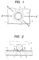
- Fig. 1 is an enlarged plan view of an essential portion showing a terminal structure of the invention
- Fig. 2 is an enlarged sectional view in a 2-2 line of Fig. 1
- Fig. 3 is an enlarged sectional view in a 3-3 line of Fig.1
- Fig. 4 is an enlarged plan view of an essential portion showing a state before a ball is soldered in the terminal structure according to the invention.
- a configuration of a terminal structure of the invention will be explained with reference to Figs. 1 through 4.
- a base material 1 made of a multi-layered substrate in which insulating thin plates are laminated or the like, not shown in the drawing in a surface and inner layers thereof, a wiring pattern made of a conductive pattern is formed and various kinds of electric components are soldered to the wiring pattern, and thereby a desired electronic circuit is formed.
- a land portion 2 made of a conductive pattern is disposed, and the land portion 2 includes a circular terminal portion 3, a circular ring-like support portion 4 disposed so as to surround the neighborhood of the outer periphery portion of the terminal portion 3, and a plurality of link portions 5 that links between the terminal portion 3 and the support portion 4 and is disposed an equi-distance apart.
- the terminal portion 3 of the land portion 2 is configured so as to connect through a connection conductor such as a through hole (not shown in the drawing) to the wiring pattern.
- an insulating layer 6 made of insulating resist is disposed, and with an entire surface 3b including an edge portion 3a located at the outer periphery portion of the terminal portion 3 exposed from the insulating layer 6, the insulating layer 6 covers an entire support portion 4 and part of the link portion 5 including the root portion connected to the support portion 4.
- the metallic ball 7 for use in the terminal has a solder film (not shown in the drawing) on a surface thereof, and the ball 7, in a state disposed on the exposed terminal portion 3, is attached to the terminal portion 3 with the solder 8.
- solder 8 is adhered to the edge portion 3a and the surface 3b of the terminal portion 3.
- the terminal structure having such configuration is configured so that, as shown in Figs. 2 and 3, on the ball 7, a member to be connected 9 made of a mother board or IC components and so on is disposed and soldered to the ball 7, and thereby an electrical connection is established.
- polygonal ones such as a square shape or the like may be used, and also in the support portion of the land portion, other than a circular shape, ring-like one having a polygonal shape may be used.
- link portion of the land portion may be allowed to dispose one, or two or more.
- the terminal structure according to the invention includes a base material having a land portion made of a conductive pattern; and a metallic ball that is used for a terminal and soldered onto the land portion; wherein the land portion includes a terminal portion for soldering the ball; a support portion disposed in the neighborhood of an outer periphery portion of the terminal portion; and a link portion for linking the terminal portion and the support portion; and wherein on the base material, with an entirety of the terminal portion including an edge portion located in the outer periphery of the terminal portion exposed, an insulating layer is disposed so as to cover the support portion; and with a solder straddled over a surface and the edge portion of the terminal portion, the ball is soldered to the terminal portion. Accordingly, the terminal structure that is large in the peel strength of the ball off the terminal portion and of the terminal portion off the base material can be obtained.
- the peel strength when the terminal portion is peeled off the base material can be made further stronger.
- the support portion is disposed so as to surround the outer periphery portion of the terminal portion, the terminal structure strong in the support of the support portion due to the insulating layer can be obtained.
- the terminal structure further stronger in the peel strength of the terminal portion off the base material can be obtained.
Landscapes
- Engineering & Computer Science (AREA)
- Microelectronics & Electronic Packaging (AREA)
- Manufacturing & Machinery (AREA)
- Electric Connection Of Electric Components To Printed Circuits (AREA)
- Coupling Device And Connection With Printed Circuit (AREA)
- Multi-Conductor Connections (AREA)
Applications Claiming Priority (2)
| Application Number | Priority Date | Filing Date | Title |
|---|---|---|---|
| JP2002037082A JP2003243813A (ja) | 2002-02-14 | 2002-02-14 | 端子構造 |
| JP2002037082 | 2002-02-14 |
Publications (2)
| Publication Number | Publication Date |
|---|---|
| EP1337134A2 true EP1337134A2 (fr) | 2003-08-20 |
| EP1337134A3 EP1337134A3 (fr) | 2005-05-04 |
Family
ID=27621434
Family Applications (1)
| Application Number | Title | Priority Date | Filing Date |
|---|---|---|---|
| EP03250776A Withdrawn EP1337134A3 (fr) | 2002-02-14 | 2003-02-07 | Structure de plage de connexion à haute résistance au pelage de plage et bille |
Country Status (5)
| Country | Link |
|---|---|
| US (1) | US20030153204A1 (fr) |
| EP (1) | EP1337134A3 (fr) |
| JP (1) | JP2003243813A (fr) |
| KR (1) | KR20030068459A (fr) |
| TW (1) | TW556455B (fr) |
Cited By (3)
| Publication number | Priority date | Publication date | Assignee | Title |
|---|---|---|---|---|
| WO2010053822A1 (fr) * | 2008-10-29 | 2010-05-14 | Corning Gilbert Inc. | Terminateur rf à circuit électrique amélioré |
| US10429376B2 (en) | 2008-05-16 | 2019-10-01 | Board Of Supervisors Of Louisiana State University And Agricultural And Mechanical College | Microfluidic isolation of tumor cells or other rare cells from whole blood or other liquids |
| US12567707B2 (en) | 2021-11-22 | 2026-03-03 | Corning Optical Communications Rf Llc | Devices, assemblies, and methods for terminating coaxial radiofrequency ports |
Families Citing this family (3)
| Publication number | Priority date | Publication date | Assignee | Title |
|---|---|---|---|---|
| JP5393986B2 (ja) | 2008-01-31 | 2014-01-22 | ピーエスフォー ルクスコ エスエイアールエル | 半導体装置の配線基板、半導体装置、電子装置及びマザーボード |
| JP5415846B2 (ja) | 2009-07-01 | 2014-02-12 | アルプス電気株式会社 | 電子回路ユニット |
| JP7519248B2 (ja) * | 2020-09-18 | 2024-07-19 | 新光電気工業株式会社 | 配線基板及びその製造方法 |
Family Cites Families (5)
| Publication number | Priority date | Publication date | Assignee | Title |
|---|---|---|---|---|
| US5519580A (en) * | 1994-09-09 | 1996-05-21 | Intel Corporation | Method of controlling solder ball size of BGA IC components |
| DE69523010T2 (de) * | 1994-10-04 | 2002-07-04 | Nec Corp., Tokio/Tokyo | Mittels automatischer Bandmontage hergestelltes Halbleitergehäuse |
| KR100216839B1 (ko) * | 1996-04-01 | 1999-09-01 | 김규현 | Bga 반도체 패키지의 솔더 볼 랜드 메탈 구조 |
| US6324754B1 (en) * | 1998-03-25 | 2001-12-04 | Tessera, Inc. | Method for fabricating microelectronic assemblies |
| JP2000138446A (ja) * | 1998-10-30 | 2000-05-16 | Nec Corp | プリント配線板の搭載部品半田付けパッド |
-
2002
- 2002-02-14 JP JP2002037082A patent/JP2003243813A/ja not_active Withdrawn
-
2003
- 2003-01-07 TW TW092100255A patent/TW556455B/zh not_active IP Right Cessation
- 2003-02-07 EP EP03250776A patent/EP1337134A3/fr not_active Withdrawn
- 2003-02-12 US US10/365,336 patent/US20030153204A1/en not_active Abandoned
- 2003-02-13 KR KR10-2003-0009007A patent/KR20030068459A/ko not_active Ceased
Cited By (5)
| Publication number | Priority date | Publication date | Assignee | Title |
|---|---|---|---|---|
| US10429376B2 (en) | 2008-05-16 | 2019-10-01 | Board Of Supervisors Of Louisiana State University And Agricultural And Mechanical College | Microfluidic isolation of tumor cells or other rare cells from whole blood or other liquids |
| WO2010053822A1 (fr) * | 2008-10-29 | 2010-05-14 | Corning Gilbert Inc. | Terminateur rf à circuit électrique amélioré |
| US8231406B2 (en) | 2008-10-29 | 2012-07-31 | Corning Gilbert Inc. | RF terminator with improved electrical circuit |
| CN102265471B (zh) * | 2008-10-29 | 2014-05-28 | 康宁吉伯股份有限公司 | 具有改进的电路的rf终接器 |
| US12567707B2 (en) | 2021-11-22 | 2026-03-03 | Corning Optical Communications Rf Llc | Devices, assemblies, and methods for terminating coaxial radiofrequency ports |
Also Published As
| Publication number | Publication date |
|---|---|
| JP2003243813A (ja) | 2003-08-29 |
| EP1337134A3 (fr) | 2005-05-04 |
| US20030153204A1 (en) | 2003-08-14 |
| TW556455B (en) | 2003-10-01 |
| TW200303157A (en) | 2003-08-16 |
| KR20030068459A (ko) | 2003-08-21 |
Similar Documents
| Publication | Publication Date | Title |
|---|---|---|
| US6404052B1 (en) | Multi-layer flexible printed wiring board | |
| JPH10308419A (ja) | 半導体パッケージ及びその半導体実装構造 | |
| JP2003017649A (ja) | 半導体装置及び半導体モジュール | |
| EP1337134A2 (fr) | Structure de plage de connexion à haute résistance au pelage de plage et bille | |
| KR100413027B1 (ko) | 테이프 캐리어 패키지 및 테이프 캐리어 패키지의 제조방법 | |
| US4925522A (en) | Printed circuit assembly with contact dot | |
| US7135204B2 (en) | Method of manufacturing a wiring board | |
| JP2002093851A (ja) | 基板の実装構造体、電気光学装置及び電子機器 | |
| JP2001015629A (ja) | 半導体装置及びその製造方法 | |
| JP2545079Y2 (ja) | 電子部品付きフレキシブル基板 | |
| JP2003069163A (ja) | フレキシブルプリント基板 | |
| JP2001156416A (ja) | フレキシブル配線基板の接続構造 | |
| JPS6330793B2 (fr) | ||
| JP2715957B2 (ja) | 混成集積回路装置 | |
| JPH04101496A (ja) | 印刷配線板 | |
| JP2650639B2 (ja) | 配線基板 | |
| JPH046212Y2 (fr) | ||
| JPH07169876A (ja) | 半導体装置及び半導体装置用実装キャリア | |
| JP2003347704A (ja) | 回路基板および表面実装型パッケージ実装方法 | |
| JP2005064159A (ja) | 電子回路ユニット | |
| JP2004207303A (ja) | 配線基板及び半導体装置並びにこれらの製造方法、回路基板並びに電子機器 | |
| JP2003209196A (ja) | 電子デバイスを実装した基板及び、電子デバイスの基板実装方法 | |
| JPH09321180A (ja) | 電子部品 | |
| JPH087953A (ja) | コネクタ及びその製造方法 | |
| WO1999050909A1 (fr) | Module convertisseur a embase pour semi-conducteur |
Legal Events
| Date | Code | Title | Description |
|---|---|---|---|
| PUAI | Public reference made under article 153(3) epc to a published international application that has entered the european phase |
Free format text: ORIGINAL CODE: 0009012 |
|
| AK | Designated contracting states |
Designated state(s): AT BE BG CH CY CZ DE DK EE ES FI FR GB GR HU IE IT LI LU MC NL PT SE SI SK TR |
|
| AX | Request for extension of the european patent |
Extension state: AL LT LV MK RO |
|
| PUAL | Search report despatched |
Free format text: ORIGINAL CODE: 0009013 |
|
| AK | Designated contracting states |
Kind code of ref document: A3 Designated state(s): AT BE BG CH CY CZ DE DK EE ES FI FR GB GR HU IE IT LI LU MC NL PT SE SI SK TR |
|
| AX | Request for extension of the european patent |
Extension state: AL LT LV MK RO |
|
| AKX | Designation fees paid |
Designated state(s): FR GB SE |
|
| REG | Reference to a national code |
Ref country code: DE Ref legal event code: 8566 |
|
| STAA | Information on the status of an ep patent application or granted ep patent |
Free format text: STATUS: THE APPLICATION IS DEEMED TO BE WITHDRAWN |
|
| 18D | Application deemed to be withdrawn |
Effective date: 20051105 |