EP1341164A2 - Vorrichtung zur Steuerung des Pegels der optischen Leistung zur Stabilisierung der Oszillation in einer Laserdiode - Google Patents
Vorrichtung zur Steuerung des Pegels der optischen Leistung zur Stabilisierung der Oszillation in einer Laserdiode Download PDFInfo
- Publication number
- EP1341164A2 EP1341164A2 EP03251002A EP03251002A EP1341164A2 EP 1341164 A2 EP1341164 A2 EP 1341164A2 EP 03251002 A EP03251002 A EP 03251002A EP 03251002 A EP03251002 A EP 03251002A EP 1341164 A2 EP1341164 A2 EP 1341164A2
- Authority
- EP
- European Patent Office
- Prior art keywords
- level
- laser diode
- erase
- optical power
- power level
- Prior art date
- Legal status (The legal status is an assumption and is not a legal conclusion. Google has not performed a legal analysis and makes no representation as to the accuracy of the status listed.)
- Withdrawn
Links
Images


Classifications
-
- G—PHYSICS
- G11—INFORMATION STORAGE
- G11B—INFORMATION STORAGE BASED ON RELATIVE MOVEMENT BETWEEN RECORD CARRIER AND TRANSDUCER
- G11B7/00—Recording or reproducing by optical means, e.g. recording using a thermal beam of optical radiation by modifying optical properties or the physical structure, reproducing using an optical beam at lower power by sensing optical properties; Record carriers therefor
- G11B7/12—Heads, e.g. forming of the optical beam spot or modulation of the optical beam
- G11B7/125—Optical beam sources therefor, e.g. laser control circuitry specially adapted for optical storage devices; Modulators, e.g. means for controlling the size or intensity of optical spots or optical traces
- G11B7/126—Circuits, methods or arrangements for laser control or stabilisation
-
- G—PHYSICS
- G11—INFORMATION STORAGE
- G11B—INFORMATION STORAGE BASED ON RELATIVE MOVEMENT BETWEEN RECORD CARRIER AND TRANSDUCER
- G11B7/00—Recording or reproducing by optical means, e.g. recording using a thermal beam of optical radiation by modifying optical properties or the physical structure, reproducing using an optical beam at lower power by sensing optical properties; Record carriers therefor
- G11B7/004—Recording, reproducing or erasing methods; Read, write or erase circuits therefor
- G11B7/006—Overwriting
Definitions
- the present invention relates to an optical power level-controlling device and more particularly to an optical power level-controlling device of an optical disk device capable of recording data on a rewritable optical disk such as CD-RW.
- Recordable optical disk may generally be categorized into write-once read-many optical disks such as CD-R and rewritable optical disks such as CD-RW.
- Fig. 1 illustrates optical power level of a laser beam used for recording data on a CD-RW.
- power level and “level” are understood to mean “optical power level”.
- the power level is varied between two values, i.e., WRITE level and ERASE level, with BIAS level being the reference level.
- the laser beam at WRITE level causes a change of state of the recording layer of the optical disk from crystalline to amorphous, thereby forming a record mark.
- the laser beam at ERASE level causes a change of state of the recording layer of the optical disk from amorphous to crystalline, thereby erasing the recorded mark.
- the laser beam is set at READ level which is at the same level as BIAS level and then a high-frequency signal of about 300 MHz is added thereon, so that the power level of the laser beam will be changed into a burst form (multi-mode).
- multi-mode a burst form
- This is due to a return optical noise caused by a laser beam that is emitted from the laser diode, reflected on the optical disk and then returned to the laser diode.
- oscillation of the diode can prevented from becoming unstable and being stopped. According to the above-mentioned multimode operation, oscillation of the laser diode can be stabilized.
- Adding a high-frequency signal of about 300MHz during a recording operation of a CD-RW as described above does not cause any problem during periods in which the laser beam is at BIAS (READ) level or at ERASE level.
- BIAS REX
- WRITE WRITE level
- an excess current may flow in the laser diode due to the high-frequency signal.
- Such an excess current may shorten life duration of the laser diode.
- the difference between ERASE level and BIAS level (labeled “DW” in Fig. 1) is indicated by a fixed value and the difference between ERASE level and WRITE level (labeled “DP” in Fig. 1) is also indicated by a fixed value. This may cause an unstable oscillation of the laser diode due to the return noise during a recording operation.
- the present invention is an optical power level-controlling device for controlling optical power level of a laser beam emitted from a light-emitting element and irradiated on an optical disk, the optical power level capable of taking an ERASE level defined as a reference level, a BIAS level lower than the ERASE level and a WRITE level higher than the ERASE level, a recording operation on the optical disk being carried out by alternating the optical power level between the BIAS level and the WRITE level, a fixed value control and a feedback control being performed on the ERASE level and on a difference between the ERASE level and the BIAS level, respectively, the device including:
- the controlling part performs a feedback control of the BIAS level while monitoring the ERASE level during a data recording operation.
- the optical power level-controlling device further includes a post-processing part for performing, as a post-process of the recording operation, a reproducing operation in a multimode in which a high-frequency signal is added on the BIAS level.
- Fig. 3 shows a block diagram of an embodiment of an optical power level-controlling device of the present invention.
- An MPU 10 controls the entire optical power level-controlling device by making use of a non-volatile memory 12 and an internal memory.
- BIAS level indication data that is output from the MPU 10 is converted into an analog form at a D/A converter 14 and is supplied to terminal "a" of a laser diode driver 16.
- ERASE level indication data i.e., DW in Fig. 1
- WRITE level indication data i.e., DP in Fig.
- the laser diode driver 16 is further provided with a terminal 22 via which modulation signals used for recording are input and a terminal 23 via which a high-frequency signal of, for example, 300 MHz for a multi-mode operation is supplied.
- the laser diode driver 16 supplies an electric current to a laser diode 24 such that the laser diode 24 emits light at an optical power level of BIAS level, ERASE level or WRITE level.
- the emitted light is irradiated on an optical disk such that data is recorded on the optical disk.
- a front monitor 26 detects power level of the laser beam that is output from the laser diode 24.
- the front monitor 26 may be a photo-diode that supplies a detected electric current corresponding to the detected power level to a collector of an npn transistor Q1.
- the transistor Q1 and npn transistors Q2 and Q3 constitutes a current mirror circuit in which detected electric currents flowing through collectors of the transistors Q2 and Q3, respectively, have the same value as the detected electric current.
- the collector of the transistor Q2 is coupled to a variable current source 32 via mutually interlocked switches 28 and 30.
- the switches 28 and 30 are operated in accordance with an instruction supplied from the MPU 10 such that they are turned on during the BIAS level period only.
- the variable current source 32 supplies a constant electric current having a value determined by the instruction supplied from the MPU 10 to the switches 28 and 30.
- a connecting point between the switches 28 and 30 is coupled to an inverted input terminal of an operational amplifier 34.
- Reference voltage Vref is supplied to a noninverted input terminal of the operational amplifier 34.
- the operational amplifier 34 and a capacitor 35 together constitute a mirror integration circuit.
- An output voltage of the mirror integration circuit is inverted at a pnp transistor 36, superimposed onto an output of the D/A converter 14 and supplied to terminal "a" of the laser diode driver 16.
- the BIAS level indication signal is supplied from the MPU 10 to the laser diode driver 16 via the D/A converter 14 and the laser diode driver 16 supplies an electric current for obtaining BIAS level to the laser diode 24.
- An indication signal corresponding to the above-mentioned BIAS level is supplied from the MPU 10 to the variable current source 32.
- An output electric current value of the variable current source 32 is, for example, i1.
- a feedback control is carried out on the power level of the laser beam emitted by the laser diode 24 in the following manner.
- the detected electric current value of the front monitor 26 is smaller than the above-mentioned electric current value i1. Accordingly, an electric current corresponding to the difference between the electric current value i1 and the detected electric current flows in such a manner that electric charge is accumulated in the capacitor 35. This causes a drop of output voltage of the operational amplifier 34 and a rise in the voltage supplied from the pnp transistor 36 to terminal "a" of the laser diode driver 16.
- the laser diode driver 16 supplies increased amount of electric current to the laser diode 24, such that the power level of the laser beam emitted from the laser diode 24 is increased.
- the laser diode driver 16 operates in a reversed manner.
- the laser diode driver 16 supplies decreased amount of electric current to the laser diode 24. This results in a drop of the power level of the laser beam emitted from the laser diode 24.
- the feed back control is achieved.
- the collector of the transistor Q3 is coupled to a variable current source 42 via mutually interlocked switches 38 and 40.
- the switches 38 and 40 operate in accordance with instructions supplied from the MPU 10 such that they are turned on during the ERASE level periods only.
- the variable current source 42 supplies a constant electric current having a value determined by the instructions supplied from the MPU 10 to the switches 38 and 40.
- a connecting point between the switches 38 and 40 is coupled to an inverted input terminal of an operational amplifier 44.
- Reference voltage Vref is supplied to a noninverted input terminal of the operational amplifier 44.
- the operational amplifier 44 and a capacitor 45 together constitute a mirror integration circuit.
- An output voltage of the mirror integration circuit is inverted at a pnp transistor 46, added onto an output of the D/A converter 14 and supplied to terminal "a" of the laser diode driver 16.
- the ERASE level indication signal is supplied from the MPU 10 to the laser diode driver 16 via the D/A converter 18 and the laser diode driver 16 supplies an electric current for obtaining ERASE level to the laser diode 24.
- an indication signal corresponding to the above-mentioned ERASE level is supplied from the MPU 10 to the variable current source 42 and an output current of the variable current source 42 is, for example, i2.
- a feedback control is carried out on the power level of the laser beam emitted by the laser diode 24 in the following manner.
- the detected electric current value of the front monitor 26 is smaller than the above-mentioned electric current value i2. Accordingly, an electric current corresponding to the difference between the electric current value i2 and the detected electric current flows in such a manner that electric charge is accumulated in the capacitor 45. This causes a drop of output voltage of the operational amplifier 44 and a rise in the voltage supplied from the pnp transistor 46 to terminal "b" of the laser diode driver 16.
- the laser diode driver 16 supplies increased amount of electric current to the laser diode 24, such that the power level of the laser beam emitted from the laser diode 24 is be increased.
- the laser diode driver 16 operates in a reversed manner.
- the laser diode driver 16 supplies decreased amount of electric current to the laser diode 24. This results in a drop of the power level of the laser beam emitted from the laser diode 24.
- the feed back control is achieved.
- Fig. 4 shows an example of a characteristic curve of output current against input voltage at terminal "b" of the laser diode driver 14 and Fig. 5 shows an example of a characteristic curve of output power level against input electric current of the laser diode 24.
- "B" indicates BIAS level
- "E” indicates ERASE level
- "W” indicates WRITE level.
- Fig. 6 is a flowchart of an embodiment of a WRITE level-setting process that is performed by the MPU 10 of the device of the present invention. This process may be performed upon loading of an optical disk into an optical disk device and at predetermined intervals thereafter.
- step S2 the MPU 10 produces a WRITE level indication data.
- the WRITE level indication data an output of the D/A converter 20 is set at 0V, the variable current source 32 is set to a predetermined value and the switches 28 and 30 are switched on to perform feedback control of the BIAS level (it is necessary that it exceeds input current level B in Fig. 5). Then, voltage at terminal "a" of the laser diode driver 16 is obtained by the A/D converter 15 and the obtained value is used as a fixed value in step S4.
- step S4 the MPU 10 generates a BIAS level indication data for setting the output of the D/A converter 14 to the above-mentioned fixed value (it is necessary that it exceeds the input electric current level B in Fig. 5). While outputting the fixed value from the D/A converter 14, the switches 28 and 30 should be switched off.
- step S6 the ERASE level indication data is used for setting the variable current source 42 to a first value (for example, a value corresponding to the output power 10 mW of the laser diode). Then, in step S8, the voltage at terminal "b" of the laser diode driver 16 is read from the A/D converter 21 and stored as voltage W1.
- step S10 the MPU 10 generates a ERASE level indication data for setting the output of the D/A converter 18 to a second value (e.g., a value corresponding to the output light power 20 mW of the laser diode).
- a second value e.g., a value corresponding to the output light power 20 mW of the laser diode.
- step S12 the voltage at terminal "b" of the laser diode driver 16 is read from the A/D converter 21 and stored as voltage W2. Then, a voltage difference (W2-W1) corresponding an increased amount 10 mW of the output optical power level is derived.
- step S14 the WRITE level indication data that is supplied to the A/D converter 20 is sequentially increased from the lowest value towards the highest value.
- the voltage at terminal "b" of the laser diode driver 16 is read from the A/D converter 21 for each value of the WRITE level indication data and is stored.
- a feedback control is performed and thus the voltage at terminal "b” gradually decreases.
- Fig. 7 is a graph showing voltage change at terminal "b" of the laser diode driver for steps S2 through S14.
- step S16 using the relationship between the voltage difference (W2-W1) and the change in power (mW) of the output power corresponding to each value of the WRITE level indication data, the actual ERASE level is for example set in a step-by-step manner from 10 mW to 20 mW.
- the corresponding ERASE level indication data (correspond to DW) is obtained for each actual ERASE level.
- a ratio DW/DP of the difference between ERASE level and BIAS level DW to the difference between WRITE level and ERASE level DP is changed in a step-by-step manner within a range of about 10% to 15%.
- the WRITE level indication data (corresponds to DP) corresponding to each of the ratio DW/DP is derived and is stored in a WRITE level table in an internal memory (volatile memory) of the MPU 10.
- step S18 the MPU 10 reads out product information (e.g., manufacturer ID) of the optical disk from the loaded optical disk.
- product information e.g., manufacturer ID
- a look-up table showing correspondence between optimum ERASE level and optimum ratio DW/DP for each product information of the optical disk is prestored in the non-volatile memory 12.
- step S20 the MPU 10 uses the product information of the optical disk to refer to the look-up table to obtain the optimum ERASE level and the optimum ratio DW/DP.
- the optimum ERASE level and the optimum ratio DW/DP are used to refer to the WRITE level table to obtain the ERASE level indication data and the WRITE level indication data used for actual recording.
- a recording operation of this optical disk can be performed with the optimum ERASE level corresponding to the recording characteristic of the loaded optical disk (CD-R) and the corresponding WRITE level. Therefore, it is possible to reduce jitter during reproduction of the optical disk.
- ERASE level indication data (corresponds to DW) is derived for each of the actual ERASE level and the ratio DW/DP of the difference DP between the ERASE level and the BIAS level to the difference DP between the WRITE level and the ERASE level is varied within a range of approximately 10% to 15% in a step-by-step manner to obtain the WRITE level indication data (corresponds to DP) to create the WRITE level table. Therefore, even if there is a change of environmental temperature or there is an aging of elements such as the laser diode 24 and front monitor 26, the ERASE level indication data and the WRITE level indication data for obtaining the actual ERASE level and the actual WRITE level can be obtained in a high accuracy. Therefore, light level control can be performed with an improved accuracy.
- the present invention can be applied to the optical power level-controlling device of the optical disk device for performing a recording operation of CD-RWs.
- "BIAS level”, "ERASE level” and “WRITE level” should be replaced by "BIAS level”, "ERASE level”, and "ERASE level”, respectively.
- a recording operation of the optical disk can be performed with the optimum erase level corresponding to the recording characteristic of the loaded optical disk (CD-RW) and corresponding optimum ERASE level. Therefore, the reproducing operation can be performed with reduced jitter.
- OPC Optimum Power Control
- PCA Power Calibration Area
- a recording operation is performed in a combined control mode in which a fixed value and a feedback control is used in such a manner that a predetermined ratio, for example about 70%, of the laser beam is determined by a fixed value and the remaining part, for example about 30%, is determined by a feed back control.
- a predetermined ratio for example about 70%
- the remaining part for example about 30%
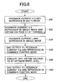
- Fig. 8 shows a flowchart of a level-setting process upon OPC performed by the MPU 10 of the present invention. This process is performed, for example, when an optical disk is loaded into an optical disk device.
- step S30 a feedback control is carried out by generating an instruction for switching on the switches 28 and 30 and for supplying an electric current of 0.7j (j is an electric current that corresponds to READ level of, for example, 1 mW) and a high-frequency signal is supplied from the terminal 23 to the laser diode driver 16 to provide a multimode reproduction state.
- step S32 while carrying out a feedback control, the supply of high-frequency signal is ceased to provide a single-mode reproduction state.
- voltage V1 at terminal "a" of the laser diode driver 16 is obtained from the A/D converter 15 and is stored in a memory in MPU 10.
- step S34 an instruction to generate an electric current of j is supplied to the variable current source 32 to carry out a feedback control and the supply of high-frequency signal is ceased to provide a single-mode reproduction state.
- step S36 the BIAS level indication data is generated.
- voltage V1 corresponds to electric current 0.7j obtained in step S32 is set to an output of the D/A converter (DAC) 14.
- an instruction to generate an electric current of j is supplied to the variable current source 32 (the setting is 1.0 mW and therefore it is required to supply an electric current corresponding to the setting to the laser diode and about 70% of the electric current is supplied from the D/A converter 14) to carry out a feedback control and the supply of high-frequency signal is ceased to provide a single-mode reproduction state. Further, a 30% feedback control is carried out and supply of high-frequency signal is ceased to provide a reproduction state of a combined control mode.
- step S38 OPC is performed to obtain the optimum WRITE level upon recording and, at the same time, voltage V2 at terminal "b" of the laser diode driver 16 at the optimum ERASE level is obtained from the A/D converter 21 and stored in a memory in the MPU 10.
- the switches 38 and 40 are switched on and an instruction to generate an electric current of k (corresponds to DW in Fig. 1) is supplied to the variable current source 42 and a feedback control of ERASE level is carried out. This is shown in Fig. 12A.
- step 40 in response to the BIAS level indication data, voltage V1 (corresponds to electric current 0.7j) obtained in step S32 is set to an output of the D/A converter (DAC) 14, an instruction to generate an electric current of j is supplied to the variable electric current source 32 to carry out a 30% feedback control and supply of high-frequency signal is ceased to provide a reproduction state of a combined control mode. Thereafter, this process is terminated.
- DAC D/A converter
- Fig. 9 shows a flowchart of a level-setting process during data recording that is performed by the MPU 10 of the present invention.
- step S52 the switches 38 and 40 are switched off and a voltage corresponding to voltage V2 derived in step S38 during OPC is set to an output of the D/A converter (DAC) 18 by the ERASE level indication data and a value obtained in the WRITE level-setting process of Fig. 6 is set to an output of the D/A converter (DAC) 20 by the WRITE level indication data.
- an instruction to generate an electric current corresponding to the optimum ERASE level is supplied to the variable electric current source 32 to carry out a data recording operation in a single mode recording state.
- BIAS level The difference between BIAS level and ERASE level is fixed by the D/A converter 18 and a feedback control is performed on BIAS level while monitoring ERASE level. This is shown in Fig. 12B.
- the feedback control of BIAS level is performed instead of a control process using sampling which cannot be performed for a high-speed recording operation since the characteristic curve shown by a solid line in Fig. 5 will be shifted to a dash-dot line if there is a temperature rise.
- step S54 post-processing is carried out in step S54.
- the switches 28 and 30 are switched on and an instruction to generate an electric current of 0.7j is supplied to the variable electric current source 32 to carry out a feedback control and high-frequency signal is supplied to the laser diode driver 16 via a terminal 23 to provide a multimode reproduction state. Thereafter, this process is terminated.
- BIAS level is controlled in a combined control mode of a fixed value control and a feedback control and ERASE and WRITE levels controlled by a fixed value control are added to BIAS level. Therefore, unstable oscillation of the laser diode due to return noise during an OPC recording operation can be prevented since the oscillation of the laser diode is stabilized as a result of a feedback control of BIAS level. Also, during a data-recording operation, oscillation of the laser diode can be stabilized by a feedback control of the BIAS level while monitoring the ERASE level.
- Fig. 10 shows a driving waveform of the laser diode (shown on an upper part of the diagram) and a focus drive waveform (shown in a lower part of the diagram) at a defective part of an optical disk during a recording operation in which BIAS level is controlled by a fixed value control in a single mode without adding a high-frequency signal as in the related art.
- amplitude of the driving waveform of the laser diode is substantially zero during period T1 that corresponding to the defective part.
- period T1 oscillation of the laser diode is ceased.
- Fig. 11 shows a driving waveform of the laser diode (shown on an upper part of the diagram) and a focus drive waveform (shown in a lower part of the diagram) at a defective part of an optical disk during a recording operation in which BIAS level is controlled in a combined control mode of fixed value control and a feedback control in a single mode without adding a high-frequency signal of the present invention.
- amplitude of the driving waveform of the laser diode becomes small during period T1 that corresponds to the defective part but is not zero. During period T2, it is achieved to prevent oscillation of the laser diode from being ceased.
Landscapes
- Physics & Mathematics (AREA)
- Optics & Photonics (AREA)
- Optical Head (AREA)
- Optical Recording Or Reproduction (AREA)
- Semiconductor Lasers (AREA)
Applications Claiming Priority (2)
| Application Number | Priority Date | Filing Date | Title |
|---|---|---|---|
| JP2002044503 | 2002-02-21 | ||
| JP2002044503 | 2002-02-21 |
Publications (2)
| Publication Number | Publication Date |
|---|---|
| EP1341164A2 true EP1341164A2 (de) | 2003-09-03 |
| EP1341164A3 EP1341164A3 (de) | 2004-12-01 |
Family
ID=27678444
Family Applications (1)
| Application Number | Title | Priority Date | Filing Date |
|---|---|---|---|
| EP03251002A Withdrawn EP1341164A3 (de) | 2002-02-21 | 2003-02-19 | Vorrichtung zur Steuerung des Pegels der optischen Leistung zur Stabilisierung der Oszillation in einer Laserdiode |
Country Status (4)
| Country | Link |
|---|---|
| US (1) | US7079460B2 (de) |
| EP (1) | EP1341164A3 (de) |
| CN (1) | CN1440031A (de) |
| TW (1) | TW200303534A (de) |
Cited By (2)
| Publication number | Priority date | Publication date | Assignee | Title |
|---|---|---|---|---|
| DE10360506A1 (de) * | 2003-10-01 | 2005-05-12 | Samsung Electro Mech | Strom/Spannungsumsetzschaltung für integrierte Fotodetektorschaltung unter Verwendung einer Verstärkungsumschaltschaltung |
| GB2397937B (en) * | 2003-01-15 | 2005-11-09 | Via Tech Inc | Apparatus and method for controlling data write operations in optical storage system |
Families Citing this family (5)
| Publication number | Priority date | Publication date | Assignee | Title |
|---|---|---|---|---|
| JP3938075B2 (ja) * | 2003-03-11 | 2007-06-27 | ヤマハ株式会社 | 光ディスク記録方法、及び光ディスク記録装置 |
| US20060239153A1 (en) * | 2005-04-25 | 2006-10-26 | Mediatek Incorporation | Methods and circuits for automatic power control |
| TW200923933A (en) * | 2007-11-23 | 2009-06-01 | Quanta Storage Inc | Method for compensating offset of laser power control circuit |
| JP4912283B2 (ja) * | 2007-11-30 | 2012-04-11 | 株式会社リコー | 半導体装置、その半導体装置を使用した半導体レーザ駆動装置及び画像形成装置 |
| JP6853477B2 (ja) * | 2017-03-31 | 2021-03-31 | ミツミ電機株式会社 | 表示装置 |
Family Cites Families (14)
| Publication number | Priority date | Publication date | Assignee | Title |
|---|---|---|---|---|
| JPS59171037A (ja) * | 1983-03-18 | 1984-09-27 | Hitachi Ltd | 半導体レーザの駆動方法及び駆動装置 |
| JPS62150732U (de) * | 1986-03-17 | 1987-09-24 | ||
| JPH0589465A (ja) * | 1991-06-28 | 1993-04-09 | Hitachi Ltd | 光学式情報記録再生方法およびその装置 |
| JPH06162507A (ja) * | 1992-11-24 | 1994-06-10 | Toshiba Corp | 情報記録方法および情報記録装置 |
| US5648952A (en) * | 1994-09-28 | 1997-07-15 | Ricoh Company, Ltd. | Phase-change optical disc recording method and apparatus, and information recording apparatus and recording pre-compensation method |
| JP3441212B2 (ja) * | 1995-01-19 | 2003-08-25 | 株式会社リコー | パワー制御方式 |
| EP0725397B1 (de) * | 1995-01-31 | 1999-09-15 | Canon Kabushiki Kaisha | Testverfahren für ein auf Pitlängenmodulation basierendes Aufzeichnungsverfahren und optisches Informationsaufzeichnungs-/wiedergabegerät welches dieses Testverfahren benutzt |
| KR100428983B1 (ko) * | 1996-02-16 | 2004-08-12 | 코닌클리케 필립스 일렉트로닉스 엔.브이. | 광정보매체기록방법및장치 |
| JP3457463B2 (ja) * | 1996-04-26 | 2003-10-20 | 富士通株式会社 | 光学的記憶装置 |
| GB2336463B (en) * | 1998-04-16 | 2000-07-05 | Ricoh Kk | Optical recording method for a rewritable phase-change optical recording medium |
| KR100322601B1 (ko) * | 1999-06-18 | 2002-03-18 | 윤종용 | 광디스크 기록 방법, 광디스크 기록 장치의 제어 방법 및 이에 적합한 광디스크 기록 장치 |
| US7212477B2 (en) * | 1999-07-23 | 2007-05-01 | Ricoh Company, Ltd. | Optical recording/reproducing apparatus with APC and SPS processes |
| US6728178B2 (en) * | 2000-10-27 | 2004-04-27 | Matsushita Electric Industrial Co., Ltd. | Semiconductor laser control method and semiconductor laser control device |
| TW508565B (en) * | 2001-03-30 | 2002-11-01 | Via Tech Inc | Power control circuit of optical information recording apparatus |
-
2003
- 2003-02-19 EP EP03251002A patent/EP1341164A3/de not_active Withdrawn
- 2003-02-19 US US10/370,438 patent/US7079460B2/en not_active Expired - Lifetime
- 2003-02-19 CN CN03104668.1A patent/CN1440031A/zh active Pending
- 2003-02-21 TW TW092103628A patent/TW200303534A/zh unknown
Cited By (3)
| Publication number | Priority date | Publication date | Assignee | Title |
|---|---|---|---|---|
| GB2397937B (en) * | 2003-01-15 | 2005-11-09 | Via Tech Inc | Apparatus and method for controlling data write operations in optical storage system |
| US7554895B2 (en) | 2003-01-15 | 2009-06-30 | Ting-Wen Su | Apparatus and method for controlling data write operations in optical storage system |
| DE10360506A1 (de) * | 2003-10-01 | 2005-05-12 | Samsung Electro Mech | Strom/Spannungsumsetzschaltung für integrierte Fotodetektorschaltung unter Verwendung einer Verstärkungsumschaltschaltung |
Also Published As
| Publication number | Publication date |
|---|---|
| US20030156512A1 (en) | 2003-08-21 |
| TW200303534A (en) | 2003-09-01 |
| CN1440031A (zh) | 2003-09-03 |
| EP1341164A3 (de) | 2004-12-01 |
| US7079460B2 (en) | 2006-07-18 |
Similar Documents
| Publication | Publication Date | Title |
|---|---|---|
| USRE42451E1 (en) | Method and device for generating a stable power control signal | |
| US6683836B2 (en) | Laser control device | |
| JP2002150590A (ja) | 光学式記録媒体による記録装置及び方法 | |
| US7079460B2 (en) | Optical power level-controlling device for stable oscillation of laser diode | |
| US7248551B2 (en) | Apparatus and method for controlling laser power for disc drive | |
| US20030099178A1 (en) | Optical disc drive and laser beam drive power supply voltage control method | |
| US6990130B2 (en) | Semiconductor laser optical output control circuit and optical device | |
| EP1339053A1 (de) | Vorrichtung zur Steuerung des Pegels der optischen Leistung zum Verringern des Jitters bei der Wiedergabe | |
| US7239590B2 (en) | Write power control method, write power control apparatus and information recording apparatus having the same | |
| US6792013B2 (en) | Auto power control circuit for laser diode | |
| US20030156521A1 (en) | Optical power level-controlling device for reduced reproduction jitter | |
| CN1534639B (zh) | 激光功率监控设备,包含该设备的光记录和/或再现装置 | |
| US7411885B2 (en) | Method of determining the time of adjusting writing strategy of an optical drive | |
| US7693022B2 (en) | Method for controlling read power and open-loop read control device using the same | |
| KR100556424B1 (ko) | 광디스크의 기록파워 제어장치 및 방법 | |
| KR20020070711A (ko) | 광기록 장치에서 기록 파워 제어장치 및 방법 | |
| KR20040000883A (ko) | 광디스크 장치에서의 기준 파워 설정방법 | |
| CN100437766C (zh) | 光盘的刻录电源控制方法 | |
| US20090180366A1 (en) | Optical disc recording apparatus | |
| US20070058507A1 (en) | Apparatus and method for controlling a recording light signal | |
| KR100682690B1 (ko) | 광디스크장치의 광원 제어장치 및 제어방법 | |
| JPH04356741A (ja) | レーザ駆動回路 | |
| KR970006886Y1 (ko) | 미니디스크플레이어의 레이저출력제어장치 | |
| JP2003317297A (ja) | 光レベル制御装置 | |
| US20070058508A1 (en) | Apparatus and method for controlling a recording light signal |
Legal Events
| Date | Code | Title | Description |
|---|---|---|---|
| PUAI | Public reference made under article 153(3) epc to a published international application that has entered the european phase |
Free format text: ORIGINAL CODE: 0009012 |
|
| AK | Designated contracting states |
Kind code of ref document: A2 Designated state(s): AT BE BG CH CY CZ DE DK EE ES FI FR GB GR HU IE IT LI LU MC NL PT SE SI SK TR |
|
| AX | Request for extension of the european patent |
Extension state: AL LT LV MK RO |
|
| PUAL | Search report despatched |
Free format text: ORIGINAL CODE: 0009013 |
|
| AK | Designated contracting states |
Kind code of ref document: A3 Designated state(s): AT BE BG CH CY CZ DE DK EE ES FI FR GB GR HU IE IT LI LU MC NL PT SE SI SK TR |
|
| AX | Request for extension of the european patent |
Extension state: AL LT LV MK RO |
|
| 17P | Request for examination filed |
Effective date: 20041108 |
|
| AKX | Designation fees paid |
Designated state(s): DE FR |
|
| 17Q | First examination report despatched |
Effective date: 20071102 |
|
| STAA | Information on the status of an ep patent application or granted ep patent |
Free format text: STATUS: THE APPLICATION IS DEEMED TO BE WITHDRAWN |
|
| 18D | Application deemed to be withdrawn |
Effective date: 20080313 |