EP1345486A2 - Boítier, respectivement paroi, d' appareil avec joint de blindage revêtu d' un conducteur - Google Patents
Boítier, respectivement paroi, d' appareil avec joint de blindage revêtu d' un conducteur Download PDFInfo
- Publication number
- EP1345486A2 EP1345486A2 EP03005329A EP03005329A EP1345486A2 EP 1345486 A2 EP1345486 A2 EP 1345486A2 EP 03005329 A EP03005329 A EP 03005329A EP 03005329 A EP03005329 A EP 03005329A EP 1345486 A2 EP1345486 A2 EP 1345486A2
- Authority
- EP
- European Patent Office
- Prior art keywords
- device housing
- wall
- shielding
- housing according
- conductive
- Prior art date
- Legal status (The legal status is an assumption and is not a legal conclusion. Google has not performed a legal analysis and makes no representation as to the accuracy of the status listed.)
- Withdrawn
Links
Images
Classifications
-
- H—ELECTRICITY
- H05—ELECTRIC TECHNIQUES NOT OTHERWISE PROVIDED FOR
- H05K—PRINTED CIRCUITS; CASINGS OR CONSTRUCTIONAL DETAILS OF ELECTRIC APPARATUS; MANUFACTURE OF ASSEMBLAGES OF ELECTRICAL COMPONENTS
- H05K9/00—Screening of apparatus or components against electric or magnetic fields
- H05K9/0007—Casings
- H05K9/0015—Gaskets or seals
-
- H—ELECTRICITY
- H05—ELECTRIC TECHNIQUES NOT OTHERWISE PROVIDED FOR
- H05K—PRINTED CIRCUITS; CASINGS OR CONSTRUCTIONAL DETAILS OF ELECTRIC APPARATUS; MANUFACTURE OF ASSEMBLAGES OF ELECTRICAL COMPONENTS
- H05K9/00—Screening of apparatus or components against electric or magnetic fields
- H05K9/0073—Shielding materials
-
- Y—GENERAL TAGGING OF NEW TECHNOLOGICAL DEVELOPMENTS; GENERAL TAGGING OF CROSS-SECTIONAL TECHNOLOGIES SPANNING OVER SEVERAL SECTIONS OF THE IPC; TECHNICAL SUBJECTS COVERED BY FORMER USPC CROSS-REFERENCE ART COLLECTIONS [XRACs] AND DIGESTS
- Y10—TECHNICAL SUBJECTS COVERED BY FORMER USPC
- Y10T—TECHNICAL SUBJECTS COVERED BY FORMER US CLASSIFICATION
- Y10T428/00—Stock material or miscellaneous articles
- Y10T428/31504—Composite [nonstructural laminate]
Definitions
- the invention relates to a device housing of an electronic Device with at least one conductive shielding gasket or wall, such as it is en masse as a telecommunications terminal (specially designed mobile phone) and is used.
- the invention has for its object a technological easy and inexpensive to manufacture device housing the above Specify the type mentioned that the existing requirements electromagnetic tightness or compatibility (EMC) is sufficient.
- EMC electromagnetic tightness or compatibility
- a Housing provided, its EMI shielding even under high grade stressful environmental conditions, for example in outdoor use, in a chemically aggressive atmosphere or in frequent Opening and resealing, high durability having.
- the production of the shielding seal is inexpensive and technologically easy possible, what to total contributes to the low cost of the housing.
- the tin alloy used is a low-Sn / Pb alloy Pb content, in particular less than 5% by mass of Pb.
- Such a composition is different from usual used solder compositions, both with regard to the conductivity as well as the mechanical and utility properties, particularly suitable for EMI shielding.
- the conductive version has a particularly high quality Coating a two-layer structure with a base layer made of a highly conductive metal, in particular copper or one Copper alloy, and the thin layer of tin or Tin alloy as a top layer.
- a base layer made of a highly conductive metal, in particular copper or one Copper alloy
- the thin layer of tin or Tin alloy as a top layer.
- the conductive coating a total thickness in the range between 0.5 ⁇ m and 10 ⁇ m. Though for special applications also thicker layers can be useful with the thickness range mentioned the required EMI properties for standard applications with relatively little material and accordingly achieve low cost.
- Another useful embodiment of the invention provides that the shielding seal or wall by a dispensed onto a carrier Elastomeres is formed. This enables one advantageous handling especially of shielding seals small cross-sections for miniaturized electronic devices, with very good mechanical resistance of the Sealing structure.
- the carrier will often be a housing part of the device, which to form a closed shielding cage itself Metal is or is coated with metal, and the conductive Surface of the shielding gasket is in contact with one further, usually also shielding, housing part stand. But it is also possible that the carrier - or also the opposite one, with the shielding seal in surface contact standing device part - a component carrier (especially a printed circuit board).
- shielding wall this is advantageous Way of several essentially superimposed Strands of the elastomer or a single high strand of elastomer, the height of which is at least twice the width, educated.
- Such shielding walls have the above for the benefits mentioned on the dispensed shield seals.
- the method of dividing the interior offers one Device housing by shielding walls formed in this way the possibility of simple and quick design changes, because a changed housing structure is without change of tools essentially solely by reprogramming a known dispensing system and the device for application the proposed conductive coating possible.
- the shielding seal or wall essentially from one thermoplastic or thermosetting polymers.
- such Polymers can be influenced by suitable additives the mechanical properties (plasticizers etc.) in their Elasticity or compression properties on the construction Adapt the required mechanical sealing effects and are well suited as carriers for the proposed shielding Coating.
- the shielding seal or wall in particular materially connected to the carrier, injection molded is. This makes separate operations to generate the basic profiles of the shielding seals or walls can be dispensed with, which further reduces the cost of housing manufacture.
- the shielding effects of the shielding seals can be or walls of devices of the above proposed kind further improve if the material of the shielding gasket or wall a filling of conductive material, in particular conductive metal and / or carbon particles - but with increased use of conductive material and with a corresponding increase in costs.
- the proposed conductive coating with tin or one Tin alloy can be made using established vacuum coating processes, in particular as a vacuum vapor deposition layer or sputter layer, in large series in high and consistent quality produce.
- the version is a "classic" spray coating (generated under atmospheric pressure) possible.
- other coating processes can also be used come, which is established for metallic or metal-containing layers are, for example galvanic or immersion processes.
- Devices of the type in question are, in particular, mobile radio terminals or other telecommunications terminals or components of cellular networks (especially base stations) that form or are sensitive to a source of EMI, or also EMI interference sensitive data communication or Data processing equipment and parts therefor. Furthermore can it is devices from the fields of sensor technology, operational measurement technology and process control technology, radio navigation devices or similar act.
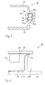
- FIG. 1 shows a section of a device housing 10 made of metal, about from deep-drawn aluminum sheet, which is a lower housing shell 11 and an upper housing shell 12, which by Fasteners not shown in the figure (for example Screws or a snap connection) connected to each other are.
- a shielding housing outer seal between the two 13 inserted.
- the housing outer seal 13 is made of two superimposed on the Bend area 11a of the lower housing shell 11 Elastomer strands 14a, 14b constructed. Of these is liable the lower strand of elastomer 14a firmly on the surface of the lower Housing shell 11, and has the upper elastomer strand 14b themselves as a result of its application immediately after education of the lower elastomer strand 14a with the same material connected.
- On the basic sealing profile formed with this 14a / 14b is initially a copper thin film as high grade conductive base layer and then a cover layer 16 of a Low lead tin alloy, all in one High vacuum coating process.
- the layer thicknesses the base layer 15 and the cover layer 16 are to be achieved the required deformability of the housing outer seal 13 on the one hand and their shielding effect on the other hand, depending on the purpose of the housing 10 also the Resistance to environmental influences (moisture, salt water or similar) must be observed.
- Fig. 2 shows schematically in a cross-sectional representation Housing section of one by means of plastic injection molding thermoplastic polymer housing 20, of which only a lower housing part 21 with a standing upright Partition 22 is shown.
- the partition 22 separates one against EMI shieldable first housing area 20A mechanically and electromagnetically sealed from a second housing area 20B from.
- the first housing area 20A is electromagnetic at the top through a conductive surface coating 26 of the circuit board 24 essentially sealed. Down and to the side the electromagnetic shielding is opened by a the left portion of the lower case 21 and the itself adjoining (left) surface of the partition 22 over the entire surface applied tin alloy layer 27 ensures.
- Shielding walls can be combined with expanded shielding seals.
- Shielding gaskets and walls are also made with one component Tin-based thin film in the same housing can be combined with those that have a two-component conductive Coating from a base layer (Cu, Ag or similar) and have a tin cover layer.
Landscapes
- Engineering & Computer Science (AREA)
- Microelectronics & Electronic Packaging (AREA)
- Shielding Devices Or Components To Electric Or Magnetic Fields (AREA)
- Casings For Electric Apparatus (AREA)
Applications Claiming Priority (2)
| Application Number | Priority Date | Filing Date | Title |
|---|---|---|---|
| DE10210577 | 2002-03-11 | ||
| DE10210577 | 2002-03-11 |
Publications (2)
| Publication Number | Publication Date |
|---|---|
| EP1345486A2 true EP1345486A2 (fr) | 2003-09-17 |
| EP1345486A3 EP1345486A3 (fr) | 2006-04-19 |
Family
ID=27762853
Family Applications (1)
| Application Number | Title | Priority Date | Filing Date |
|---|---|---|---|
| EP20030005329 Withdrawn EP1345486A3 (fr) | 2002-03-11 | 2003-03-11 | Boîtier, respectivement paroi, d' appareil avec joint de blindage revêtu d' un conducteur |
Country Status (4)
| Country | Link |
|---|---|
| US (1) | US20040071970A1 (fr) |
| EP (1) | EP1345486A3 (fr) |
| CN (1) | CN1444439A (fr) |
| DE (1) | DE10310598A1 (fr) |
Cited By (2)
| Publication number | Priority date | Publication date | Assignee | Title |
|---|---|---|---|---|
| WO2009005584A3 (fr) * | 2007-07-03 | 2009-02-19 | Gore Enterprise Holdings Inc | Joint emi et borne de mise à la terre soudables |
| US20250131945A1 (en) * | 2021-08-27 | 2025-04-24 | Nhk Spring Co., Ltd. | Cover and recording device |
Families Citing this family (7)
| Publication number | Priority date | Publication date | Assignee | Title |
|---|---|---|---|---|
| WO2010065035A1 (fr) * | 2008-12-04 | 2010-06-10 | Hewlett-Packard Development Company, L.P. | Enveloppe stratifiée en carbone |
| US8842039B2 (en) * | 2012-05-23 | 2014-09-23 | Rosemount Tank Radar Ab | Guided wave radar level gauge with improved sealing arrangement |
| FR3003428B1 (fr) * | 2013-03-12 | 2016-11-04 | Plastic Omnium Cie | Caisson d'hebergement d'equipement de puissance de vehicule automobile formant blindage electromagnetique |
| CN106572292A (zh) * | 2016-11-10 | 2017-04-19 | 协创数据技术股份有限公司 | 一种具有防抖动功能的全景相机 |
| DE102018208925A1 (de) | 2018-06-06 | 2019-12-12 | Bayerische Motoren Werke Aktiengesellschaft | Verfahren zum Abschirmen von Bauteilen |
| US11017820B1 (en) * | 2020-02-21 | 2021-05-25 | Seagate Technology Llc | Electromagnetic shielding for electronic devices |
| DE102022207527A1 (de) | 2022-07-22 | 2024-01-25 | Volkswagen Aktiengesellschaft | Dichtungsanordnung in einem Elektronikgehäuse |
Family Cites Families (19)
| Publication number | Priority date | Publication date | Assignee | Title |
|---|---|---|---|---|
| US4467002A (en) * | 1981-12-15 | 1984-08-21 | Raychem Limited | Dimensionally-recoverable article |
| US4678863A (en) * | 1985-06-27 | 1987-07-07 | Rca Corporation | Corrosion resistant conductive elastomers |
| JPH0787275B2 (ja) * | 1988-10-28 | 1995-09-20 | 北川工業株式会社 | 導電性シール材 |
| US5045635A (en) * | 1989-06-16 | 1991-09-03 | Schlegel Corporation | Conductive gasket with flame and abrasion resistant conductive coating |
| US5222294A (en) * | 1990-12-03 | 1993-06-29 | Motorola, Inc. | High isolation packaging method |
| GB9111633D0 (en) * | 1991-05-30 | 1991-07-24 | Raychem Ltd | Dimensionally-recoverable article |
| DE4319965C3 (de) * | 1993-06-14 | 2000-09-14 | Emi Tec Elektronische Material | Verfahren zur Herstellung eines Gehäuses mit elektromagnetischer Abschirmung |
| CA2129073C (fr) * | 1993-09-10 | 2007-06-05 | John P. Kalinoski | Joints moulants iem |
| US5573857A (en) * | 1995-09-29 | 1996-11-12 | Neptco Incorporated | Laminated shielding tape |
| EP0875130B1 (fr) * | 1996-01-19 | 2006-06-07 | Bernd Tiburtius | Boitier a effet de blindage electrique |
| US5804762A (en) * | 1996-03-22 | 1998-09-08 | Parker-Hannifin Corporation | EMI shielding gasket having shear surface attachments |
| DE29706914U1 (de) * | 1997-04-17 | 1997-06-19 | REHAU AG + Co., 95111 Rehau | Gehäuseteil aus Kunststoff |
| US5847317A (en) * | 1997-04-30 | 1998-12-08 | Ericsson Inc. | Plated rubber gasket for RF shielding |
| US5881945A (en) * | 1997-04-30 | 1999-03-16 | International Business Machines Corporation | Multi-layer solder seal band for semiconductor substrates and process |
| US6255581B1 (en) * | 1998-03-31 | 2001-07-03 | Gore Enterprise Holdings, Inc. | Surface mount technology compatible EMI gasket and a method of installing an EMI gasket on a ground trace |
| JP2003523621A (ja) * | 2000-02-18 | 2003-08-05 | パーカー−ハニフイン・コーポレーシヨン | 低閉じ力、現場形成型、イーエムアイ遮蔽ガスケットの製法 |
| WO2001065903A2 (fr) * | 2000-02-28 | 2001-09-07 | Amesbury Group, Inc. | Procede et dispositif d'antiparasitage |
| US6541698B2 (en) * | 2001-03-13 | 2003-04-01 | Schlegel Systems, Inc. | Abrasion resistant conductive film and gasket |
| US6809254B2 (en) * | 2001-07-20 | 2004-10-26 | Parker-Hannifin Corporation | Electronics enclosure having an interior EMI shielding and cosmetic coating |
-
2003
- 2003-03-11 CN CN03122697A patent/CN1444439A/zh active Pending
- 2003-03-11 EP EP20030005329 patent/EP1345486A3/fr not_active Withdrawn
- 2003-03-11 US US10/386,368 patent/US20040071970A1/en not_active Abandoned
- 2003-03-11 DE DE2003110598 patent/DE10310598A1/de not_active Ceased
Cited By (2)
| Publication number | Priority date | Publication date | Assignee | Title |
|---|---|---|---|---|
| WO2009005584A3 (fr) * | 2007-07-03 | 2009-02-19 | Gore Enterprise Holdings Inc | Joint emi et borne de mise à la terre soudables |
| US20250131945A1 (en) * | 2021-08-27 | 2025-04-24 | Nhk Spring Co., Ltd. | Cover and recording device |
Also Published As
| Publication number | Publication date |
|---|---|
| DE10310598A1 (de) | 2003-10-09 |
| CN1444439A (zh) | 2003-09-24 |
| US20040071970A1 (en) | 2004-04-15 |
| EP1345486A3 (fr) | 2006-04-19 |
Similar Documents
| Publication | Publication Date | Title |
|---|---|---|
| DE69508911T2 (de) | Gehäuse mit elektromagnetischer Abschirmung | |
| DE69301407T2 (de) | Festelektrolytkondensator in Chip-Bauweise | |
| DE19880257B4 (de) | Verfahren zur Herstellung eines Abschirmgehäuses | |
| DE2608921A1 (de) | Abschirmstreifen fuer elektromagnetische stoerungen | |
| DE2655659B2 (de) | Elektrisches Bauelement, insbesondere Trockenelektrolytkondensator | |
| DE102014117410B4 (de) | Elektrisches Kontaktelement, Einpressstift, Buchse und Leadframe | |
| DE19733627C1 (de) | Elektrisch leitfähige Dichtung und Verfahren zu deren Herstellung | |
| EP1055356B1 (fr) | Boitier | |
| EP1345486A2 (fr) | Boítier, respectivement paroi, d' appareil avec joint de blindage revêtu d' un conducteur | |
| DE112008001092T5 (de) | Schutzabdeckung für einen Schaltungsträger | |
| DE19851037B4 (de) | Magnetfelddetektor | |
| DE10310604A1 (de) | Gerätegehäuse mit einem elektromagnetisch abgeschirmten Raumbereich | |
| DE3815517A1 (de) | Dichtung fuer ein elektromagnetische strahlung abschirmendes gehaeuse | |
| DE102007046913A1 (de) | Abdichtbares Leiterplattengehäuse sowie Leiterplatte zur Verwendung in dem Leiterplattengehäuse | |
| EP0192818B1 (fr) | Condensateur bobiné à feuille plastique réalisé sous forme de pastille | |
| DE102008058287B4 (de) | Elektronisches Modul mit einem Dichtelement und Verfahren zum Herstellen des Moduls | |
| DE2433613A1 (de) | Durchfuehrungsanschluss fuer ein elektrisches bauelement sowie verfahren zu dessen herstellung | |
| EP1481408A2 (fr) | Condensateur dote d'une couche d'adherence au niveau de son contact de cathode | |
| DE1591581A1 (de) | Mikrowellen-Schaltkreis in Triplate-Technik | |
| DE10060917A1 (de) | Abschirmung gegen elektromagnetische Strahlung | |
| EP2463900A2 (fr) | Procédé de fabrication d'un agencement de commutation | |
| DE4345594B4 (de) | Verfahren zur Herstellung eines eine Abschirmung gegen elektromagnetische Abstrahlung aufweisenden Gehäuses | |
| DE202008015475U1 (de) | Sammeldichtung für Steckverbindergehäuse | |
| DE9420980U1 (de) | Zum Aufnehmen von elektronischen und/oder mikromechanischen Bauteilen bestimmtes Gehäuse aus einem Hartkunststoff, ins welches Leiterbahnen hineinführen | |
| DE102024207783A1 (de) | Abschirmgehäuse und Verfahren zum Ausbilden eines Abschirmgehäuses |
Legal Events
| Date | Code | Title | Description |
|---|---|---|---|
| PUAI | Public reference made under article 153(3) epc to a published international application that has entered the european phase |
Free format text: ORIGINAL CODE: 0009012 |
|
| AK | Designated contracting states |
Kind code of ref document: A2 Designated state(s): AT BE BG CH CY CZ DE DK EE ES FI FR GB GR HU IE IT LI LU MC NL PT SE SI SK TR |
|
| AX | Request for extension of the european patent |
Extension state: AL LT LV MK RO |
|
| PUAL | Search report despatched |
Free format text: ORIGINAL CODE: 0009013 |
|
| AK | Designated contracting states |
Kind code of ref document: A3 Designated state(s): AT BE BG CH CY CZ DE DK EE ES FI FR GB GR HU IE IT LI LU MC NL PT SE SI SK TR |
|
| AX | Request for extension of the european patent |
Extension state: AL LT LV MK RO |
|
| 17P | Request for examination filed |
Effective date: 20060823 |
|
| AKX | Designation fees paid |
Designated state(s): DE FR GB |
|
| 17Q | First examination report despatched |
Effective date: 20071019 |
|
| STAA | Information on the status of an ep patent application or granted ep patent |
Free format text: STATUS: THE APPLICATION IS DEEMED TO BE WITHDRAWN |
|
| 18D | Application deemed to be withdrawn |
Effective date: 20090630 |