EP1346371B1 - Circuit d'echantillonnage-blocage basse tension a compression et expansion de plage de tension - Google Patents
Circuit d'echantillonnage-blocage basse tension a compression et expansion de plage de tension Download PDFInfo
- Publication number
- EP1346371B1 EP1346371B1 EP01272181A EP01272181A EP1346371B1 EP 1346371 B1 EP1346371 B1 EP 1346371B1 EP 01272181 A EP01272181 A EP 01272181A EP 01272181 A EP01272181 A EP 01272181A EP 1346371 B1 EP1346371 B1 EP 1346371B1
- Authority
- EP
- European Patent Office
- Prior art keywords
- voltage
- data signal
- sampled
- field effect
- transistor
- Prior art date
- Legal status (The legal status is an assumption and is not a legal conclusion. Google has not performed a legal analysis and makes no representation as to the accuracy of the status listed.)
- Expired - Lifetime
Links
Images

Classifications
-
- H—ELECTRICITY
- H03—ELECTRONIC CIRCUITRY
- H03M—CODING; DECODING; CODE CONVERSION IN GENERAL
- H03M1/00—Analogue/digital conversion; Digital/analogue conversion
- H03M1/12—Analogue/digital converters
- H03M1/50—Analogue/digital converters with intermediate conversion to time interval
- H03M1/54—Input signal sampled and held with linear return to datum
-
- H—ELECTRICITY
- H03—ELECTRONIC CIRCUITRY
- H03M—CODING; DECODING; CODE CONVERSION IN GENERAL
- H03M1/00—Analogue/digital conversion; Digital/analogue conversion
- H03M1/12—Analogue/digital converters
- H03M1/124—Sampling or signal conditioning arrangements specially adapted for A/D converters
- H03M1/129—Means for adapting the input signal to the range the converter can handle, e.g. limiting, pre-scaling ; Out-of-range indication
-
- G—PHYSICS
- G11—INFORMATION STORAGE
- G11C—STATIC STORES
- G11C27/00—Electric analogue stores, e.g. for storing instantaneous values
- G11C27/02—Sample-and-hold arrangements
-
- G—PHYSICS
- G11—INFORMATION STORAGE
- G11C—STATIC STORES
- G11C27/00—Electric analogue stores, e.g. for storing instantaneous values
- G11C27/02—Sample-and-hold arrangements
- G11C27/024—Sample-and-hold arrangements using a capacitive memory element
Definitions
- the invention relates to an electronic circuit comprising a sample and hold circuit for sampling and holding an input data signal, comprising compression means arranged and configured to compress a voltage range of the input data signal and convert the input data signal into a compressed data voltage to be sampled, and further comprises expansion means for converting a sampled voltage into a sampled output data signal.
- Such electronic circuits are known from the prior art and are used inter alia in various types of analog-to-digital converters. There is a general trend in the design of electronic circuits toward operation at low supply voltages.
- the minimum required supply voltage in known sample and hold circuits is equal to or higher than the maximum value of the sampled voltage which corresponds to a maximum voltage of the input data signal.
- DE-C-4409063 describes an electronic circuit on which an analogue input signal is compressed before application, via a sample and hold circuit, to an ADC. The resultant digital signal is applied to a digital correction circuit, which outputs a digital output signal which is proportional to the analogue input signal.
- the invention is defined by the independent claim.
- the dependent claim describes an advantageous embodiment.
- the electronic circuit mentioned in the opening paragraph comprises switching means for sampling the compressed data voltage which corresponds to the input data signal, a capacitive element for temporarily holding the sampled voltage
- the compression means comprises a first transistor with a main current path which is designed to pass a current which is linearly dependent on the input data signal, a control voltage of the first transistor constituting the data voltage to be sampled in the operational state
- the expansion means is operable to convert the sampled voltage into a sampled output data signal which corresponds linearly to the input data signal and comprises a second transistor such that the sampled voltage constitutes a control voltage for the second transistor in the operational state, while the second transistor comprises a main current path for supplying the sampled output data signal.
- the presence of the compression means in the electronic circuit of the invention reduces the maximum value of the sampled voltage across the capacitive element. As a result, the electronic circuit can operate at a lower supply voltage. Furthermore, because the expansion means supplies a current, which is dependent linearly on the input data signal, the output data signal is undistorted, while nevertheless the electronic circuit can operate at a lower supply voltage.
- the first and second transistors are mutually matched, so that they in fact form a current mirror, i.e. the output current of the current mirror is sampled version of the input current of the current mirror.
- the first and second transistor may be constructed as bipolar transistors or as field effect transistors.
- Fig. 1 is a diagram showing the principle of the sample and hold circuit according to the invention.
- the circuit comprises compression means CPR, switching means S under the control of a clock signal CLK, a capacitive element constructed with a capacitor T 1 , and expansion means EXP.
- the compression means CPR receive an input data signal in the form of an input voltage U;, or an input current I i and convert this input data signal into a compressed data voltage U 1 .
- the data voltage U 1 is sampled by the switching means S such that a sampled voltage U C1 arises which is held by the capacitor C 1 .
- the sampled U C1 is converted by the expansion means into an output data signal formed by the output current I 0 .
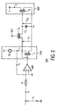
- Fig. 2 is a circuit diagram of an embodiment of a sample and hold circuit S/H according to the invention.
- the compression means CPR are constructed with a first field effect transistor T 1 and a current source CS for providing a DC current through the first field effect transistor T 1 .
- the expansion means CPR are constructed with a second field effect transistor T 2 .
- the sample and hold circuit S/H further comprises an amplifier AMP with a non-inverting input, an inverting input, and an output, a resistor R, a field effect transistor T s which forms the switching means of Fig. 2, and the capacitor C 1 .
- the resistor R is connected between an input terminal 1 and the non-inverting input of the amplifier AMP.
- the first field effect transistor T 1 is connected by a gate to the output of the amplifier AMP.
- the source of the transistor T 1 is connected to a reference voltage.
- the drain of the transistor T 1 is connected to the current source CS and to the non-inverting input of the amplifier AMP.
- a switching transistor, constructed with a field effect transistor T s in this example, is connected by a source to the gate of the first field effect transistor T 1 and by a drain to the gate of the second field effect transistor T 2 .
- the gate of the transistor T s receives a clock signal so as to be able to sample the data voltage U 1 which is present between the gate and the source of the first field effect transistor T 1 and to supply the sampled voltage U c1 to the capacitor C 1 .
- the circuit operates as follows.
- the amplifier AMP and the field effect transistor T 1 form a negative feedback system, so that the non-inverting input of the amplifier AMP forms a so-called virtual ground.
- the input voltage U i is converted via the resistor R into an input current I i which flows through the drain-source path of the first transistor T 1 .
- This generates a gate-source voltage between the gate and the source of the first transistor T 1 which constitutes the data voltage U 1 .
- the data voltage U 1 is a compressed version of the input voltage U i . It is also possible, more directly , to have a data input current I i flow through the drain-source path of the first field effect transistor T 1 .
- the data voltage U 1 is sampled by means of the field effect transistor T s , which acts as a switch, so that the sampled voltage is temporarily stored in the capacitor C 1 .
- the second field effect transistor T 2 converts this sampled voltage U c1 into an output current I 0 . Since the first and the second field effect transistors T 1 and T 2 are mutually matched, the output current I 0 is linear with respect to the input current I i , and accordingly also with respect to the input voltage U i .
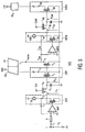
- Fig. 3 is a circuit diagram of an analog-to-digital converter ADC which comprises two sample and hold circuits in accordance with the principle of Fig. 2.
- the elements of the second sample and hold circuit have been given the same reference symbols, but with the addition of the letter B.
- the actual analog-to-digital converter is built up from a first part of the ADC for generating the most significant bits and a second part of the ADC for generating the less significant (remaining) bits.
- the first and the second part are usually denoted the coarse and the fine part, respectively.
- the ADC further comprises a field effect transistor T 3 which is connected by a gate to the gate of the second field effect transistor T 2 and by a source to the source of the second field effect transistor T 2 .
- a same current I 0 flows in the drain-source path of the third transistor T 3 as in the drain-source path of the second transistor T 2 .
- the current I 0 supplied by the second transistor T 2 is converted by the coarse analog-to-digital converter AD 1 into the most significant bits, which are denoted MSB. These bits MSB are supplied to a digital-to-analog converter DA for supplying a so-called coarse current I coarse .
- the difference between the current I coarse and I 0 supplied by the transistor T 3 is denoted I res .
- I res is the so-called residue and contains information on the LSB bits of the analog-to-digital converter ADC yet to be generated.
- the residue I res is supplied to the input of the second sample and hold circuit and is treated in the same manner as the input current I i in the first sample and hold circuit.
- the transistor T 2B finally, supplies the current denoted I 0B , which is converted by the fine analog-to-digital converter AD 2 so as to deliver the least significant bits, which are denoted LSB.
- the bits MSB and LSB together form the complete digital word.
- the electronic circuit may be implemented with discrete components or may be used as part of an integrated circuit.
- Field effect transistors may be replaced by bipolar transistors. It is also possible to replace all N-conductivity type transistors by P-conductivity type transistors.
Landscapes
- Engineering & Computer Science (AREA)
- Theoretical Computer Science (AREA)
- Analogue/Digital Conversion (AREA)
- Oscillators With Electromechanical Resonators (AREA)
- Superconductors And Manufacturing Methods Therefor (AREA)
- Liquid Crystal Display Device Control (AREA)
Claims (2)
- Circuit électronique comprenant un circuit échantillon et maintien (S/H) pour échantillonner et maintenir un signal de données d'entrée (Ui, Ii) comprenant des moyens de compression (CPR) disposés et configurés pour comprimer une plage de tensions du signal de données d'entrée (Ui) et convertir ledit signal de données d'entrée en une tension de données comprimée (U1) à échantillonner, et des moyens d'expansion (EXP) pour convertir une tension échantillonnée (UC1) en un signal de données de sortie échantillonné (I0), le circuit électronique étant caractérisé par le fait de comprendre des moyens de commutation (S, TS) pour échantillonner la tension de données comprimée (U1) qui correspond au signal de données d'entrée (Ui, Ii) et un élément capacitif (C1) pour maintenir provisoirement la tension échantillonnée (UC1) ; et en ce que les moyens de compression (CPR) comprennent un premier transistor (T1) avec une voie de courant principal qui est conçue pour faire passer le courant qui est linéairement fonction du signal de données d'entrée (Ui, Ii), une tension de commande du premier transistor (T1) constituant la tension de données (U1) à échantillonner à l'état opérationnel, et en ce que les moyens d'expansion (EXP) peuvent être actionnés pour convertir la tension échantillonnée (UC1) en un signal de données de sortie échantillonné (I0) qui correspond linéairement au signal de données d'entrée (Ui, Ii) et comprend un second transistor (T2), de telle sorte que la tension échantillonnée (UC1) constitue une tension de commande pour le second transistor (T2) à l'état de fonctionnement, tandis que le second transistor (T2) comprend une voie de courant principal pour alimenter le signal de données de sortie échantillonné (I0).
- Convertisseur analogique en numérique comprenant le circuit électronique de la revendication 1, ledit convertisseur présentant une entrée pour recevoir ledit signal de données de sortie échantillonné (I0) provenant dudit circuit d'échantillon et de maintien (S/H).
Priority Applications (1)
| Application Number | Priority Date | Filing Date | Title |
|---|---|---|---|
| EP01272181A EP1346371B1 (fr) | 2000-12-22 | 2001-12-11 | Circuit d'echantillonnage-blocage basse tension a compression et expansion de plage de tension |
Applications Claiming Priority (4)
| Application Number | Priority Date | Filing Date | Title |
|---|---|---|---|
| EP00204796 | 2000-12-22 | ||
| EP00204796 | 2000-12-22 | ||
| EP01272181A EP1346371B1 (fr) | 2000-12-22 | 2001-12-11 | Circuit d'echantillonnage-blocage basse tension a compression et expansion de plage de tension |
| PCT/IB2001/002517 WO2002052574A1 (fr) | 2000-12-22 | 2001-12-11 | Circuit d'echantillonnage-blocage basse tension a compression et expansion de plage de tension |
Publications (2)
| Publication Number | Publication Date |
|---|---|
| EP1346371A1 EP1346371A1 (fr) | 2003-09-24 |
| EP1346371B1 true EP1346371B1 (fr) | 2007-12-12 |
Family
ID=8172555
Family Applications (1)
| Application Number | Title | Priority Date | Filing Date |
|---|---|---|---|
| EP01272181A Expired - Lifetime EP1346371B1 (fr) | 2000-12-22 | 2001-12-11 | Circuit d'echantillonnage-blocage basse tension a compression et expansion de plage de tension |
Country Status (7)
| Country | Link |
|---|---|
| US (1) | US6549043B2 (fr) |
| EP (1) | EP1346371B1 (fr) |
| JP (1) | JP3986963B2 (fr) |
| KR (1) | KR100919372B1 (fr) |
| AT (1) | ATE381102T1 (fr) |
| DE (1) | DE60131892T2 (fr) |
| WO (1) | WO2002052574A1 (fr) |
Families Citing this family (7)
| Publication number | Priority date | Publication date | Assignee | Title |
|---|---|---|---|---|
| EP1328945B9 (fr) * | 2000-08-04 | 2010-06-23 | Infineon Technologies AG | Circuit echantillonneur bloqueur de courant, convertisseur analogique/numerique et procede pour exploiter un circuit echantillonneur bloqueur de courant |
| US6798253B1 (en) * | 2003-04-18 | 2004-09-28 | Windbound Electronics Corporation | Signal sorting device and method |
| JP2006101479A (ja) * | 2004-09-02 | 2006-04-13 | Canon Inc | 固体撮像装置及びそれを用いたカメラ |
| US7891570B2 (en) * | 2007-02-28 | 2011-02-22 | Microvision, Inc. | Photodiode with improved performance in ambient light |
| CN102291146B (zh) * | 2011-04-22 | 2013-11-27 | 四川和芯微电子股份有限公司 | 采样保持电路及方法 |
| CN103762985B (zh) * | 2014-01-16 | 2017-04-12 | 四川和芯微电子股份有限公司 | 采样保持电路 |
| US11521693B2 (en) * | 2021-02-05 | 2022-12-06 | Nxp B.V. | Sample and hold circuit for current |
Family Cites Families (8)
| Publication number | Priority date | Publication date | Assignee | Title |
|---|---|---|---|---|
| US3708624A (en) * | 1969-04-24 | 1973-01-02 | Vicom Corp | Pulse code modulation communication system |
| US4528549A (en) * | 1983-01-27 | 1985-07-09 | The United States Of America As Represented By The Secretary Of The Air Force | Bipolar digitizer having compression capability |
| DE8717485U1 (de) * | 1987-10-06 | 1989-04-06 | ANT Nachrichtentechnik GmbH, 7150 Backnang | Dynamikkompressor |
| US5162670A (en) * | 1990-01-26 | 1992-11-10 | Kabushiki Kaisha Toshiba | Sample-and-hold circuit device |
| DE69420631T2 (de) * | 1993-06-02 | 2000-04-06 | Canon K.K. | Signalverarbeitungsvorrichtung |
| DE4409063C1 (de) * | 1994-03-11 | 1995-08-10 | Imc Messysteme Gmbh | Schaltungsanordnung zur Analog-Digital-Wandlung |
| US5736879A (en) * | 1996-02-02 | 1998-04-07 | Siliconix Incorporated | Closed-loop frequency-to-current converter with integrable capacitances |
| WO1999040682A2 (fr) * | 1998-02-03 | 1999-08-12 | Koninklijke Philips Electronics N.V. | Circuit d'entree combine |
-
2001
- 2001-12-11 DE DE60131892T patent/DE60131892T2/de not_active Expired - Lifetime
- 2001-12-11 KR KR1020027010902A patent/KR100919372B1/ko not_active Expired - Fee Related
- 2001-12-11 AT AT01272181T patent/ATE381102T1/de not_active IP Right Cessation
- 2001-12-11 JP JP2002553783A patent/JP3986963B2/ja not_active Expired - Fee Related
- 2001-12-11 EP EP01272181A patent/EP1346371B1/fr not_active Expired - Lifetime
- 2001-12-11 WO PCT/IB2001/002517 patent/WO2002052574A1/fr not_active Ceased
- 2001-12-20 US US10/024,755 patent/US6549043B2/en not_active Expired - Lifetime
Non-Patent Citations (1)
| Title |
|---|
| None * |
Also Published As
| Publication number | Publication date |
|---|---|
| EP1346371A1 (fr) | 2003-09-24 |
| KR100919372B1 (ko) | 2009-09-25 |
| DE60131892D1 (de) | 2008-01-24 |
| WO2002052574A1 (fr) | 2002-07-04 |
| ATE381102T1 (de) | 2007-12-15 |
| JP3986963B2 (ja) | 2007-10-03 |
| DE60131892T2 (de) | 2008-04-30 |
| US6549043B2 (en) | 2003-04-15 |
| US20020079934A1 (en) | 2002-06-27 |
| JP2004517522A (ja) | 2004-06-10 |
| KR20030001364A (ko) | 2003-01-06 |
Similar Documents
| Publication | Publication Date | Title |
|---|---|---|
| CN101133556B (zh) | 乘法数字到模拟转换器及包含其的管线模拟到数字转换器 | |
| US5691720A (en) | Delta sigma analog-to-digital converter having programmable resolution/bias current circuitry and method | |
| KR100824793B1 (ko) | 기준 전압을 스스로 공급하는 파이프라인 구조의 아날로그디지털 컨버터 | |
| JP2916505B2 (ja) | 比較回路 | |
| US20100156688A1 (en) | Multiplying digital-to-analog converter | |
| JPH0656957B2 (ja) | 広範囲の基準電圧に対して正確なd/a変換器 | |
| EP1346371B1 (fr) | Circuit d'echantillonnage-blocage basse tension a compression et expansion de plage de tension | |
| EP0466145B1 (fr) | Convertisseur numérique-analogique | |
| GB2401497A (en) | A wideband switched-capacitor CMOS voltage comparator for a sub-ranging ADC | |
| US5313206A (en) | Sub-ranging analogue to digital converter using differential signals and direct current subtraction | |
| US7501972B2 (en) | Reference voltage generation circuit and pipe line analog-to-digital converter using the same | |
| US20090073016A1 (en) | Pipelined analog-to-digital converter | |
| EP0761037B1 (fr) | Amplificateur differentiel a compensation dependant du signal et convertisseur a/n plurietage a double residu comportant ce meme amplificateur differentiel | |
| US5689260A (en) | Analog-to-digital converter using scaled signal to initialize coarse conversion circuit | |
| CN110890891A (zh) | 数字至模拟转换器 | |
| US6639430B2 (en) | High speed latch comparators | |
| TWI407701B (zh) | 具受控緩衝輸入之數位至類比轉換器 | |
| EP0558243A2 (fr) | Convertisseur numérique-analogique produisant une sortie linéaire précise aussi bien pour des entrées de signal numérique positives que négatives | |
| JP2005268901A (ja) | 半導体集積回路 | |
| US20050038846A1 (en) | Substraction circuit with a dummy digital to analog converter | |
| KR101939147B1 (ko) | 가변 기준전압 발생회로 및 이를 포함한 아날로그 디지털 변환기 | |
| US10483993B1 (en) | Residue amplifier | |
| CN101741356A (zh) | 比较器与流水线模数转换器 | |
| KR19990007013A (ko) | 아날로그 디지털 변환기 | |
| US20240204686A1 (en) | Integrated circuit comprising a digital-to-analog converter |
Legal Events
| Date | Code | Title | Description |
|---|---|---|---|
| PUAI | Public reference made under article 153(3) epc to a published international application that has entered the european phase |
Free format text: ORIGINAL CODE: 0009012 |
|
| 17P | Request for examination filed |
Effective date: 20030722 |
|
| AK | Designated contracting states |
Kind code of ref document: A1 Designated state(s): AT BE CH CY DE DK ES FI FR GB GR IE IT LI LU MC NL PT SE TR |
|
| 17Q | First examination report despatched |
Effective date: 20050725 |
|
| GRAP | Despatch of communication of intention to grant a patent |
Free format text: ORIGINAL CODE: EPIDOSNIGR1 |
|
| RAP1 | Party data changed (applicant data changed or rights of an application transferred) |
Owner name: NXP B.V. |
|
| GRAS | Grant fee paid |
Free format text: ORIGINAL CODE: EPIDOSNIGR3 |
|
| GRAA | (expected) grant |
Free format text: ORIGINAL CODE: 0009210 |
|
| AK | Designated contracting states |
Kind code of ref document: B1 Designated state(s): AT BE CH CY DE DK ES FI FR GB GR IE IT LI LU MC NL PT SE TR |
|
| REG | Reference to a national code |
Ref country code: GB Ref legal event code: FG4D |
|
| REG | Reference to a national code |
Ref country code: CH Ref legal event code: EP |
|
| REG | Reference to a national code |
Ref country code: IE Ref legal event code: FG4D |
|
| REF | Corresponds to: |
Ref document number: 60131892 Country of ref document: DE Date of ref document: 20080124 Kind code of ref document: P |
|
| PG25 | Lapsed in a contracting state [announced via postgrant information from national office to epo] |
Ref country code: LI Free format text: LAPSE BECAUSE OF FAILURE TO SUBMIT A TRANSLATION OF THE DESCRIPTION OR TO PAY THE FEE WITHIN THE PRESCRIBED TIME-LIMIT Effective date: 20071212 Ref country code: SE Free format text: LAPSE BECAUSE OF FAILURE TO SUBMIT A TRANSLATION OF THE DESCRIPTION OR TO PAY THE FEE WITHIN THE PRESCRIBED TIME-LIMIT Effective date: 20080312 Ref country code: CH Free format text: LAPSE BECAUSE OF FAILURE TO SUBMIT A TRANSLATION OF THE DESCRIPTION OR TO PAY THE FEE WITHIN THE PRESCRIBED TIME-LIMIT Effective date: 20071212 |
|
| PG25 | Lapsed in a contracting state [announced via postgrant information from national office to epo] |
Ref country code: FI Free format text: LAPSE BECAUSE OF FAILURE TO SUBMIT A TRANSLATION OF THE DESCRIPTION OR TO PAY THE FEE WITHIN THE PRESCRIBED TIME-LIMIT Effective date: 20071212 Ref country code: NL Free format text: LAPSE BECAUSE OF FAILURE TO SUBMIT A TRANSLATION OF THE DESCRIPTION OR TO PAY THE FEE WITHIN THE PRESCRIBED TIME-LIMIT Effective date: 20071212 |
|
| NLV1 | Nl: lapsed or annulled due to failure to fulfill the requirements of art. 29p and 29m of the patents act | ||
| REG | Reference to a national code |
Ref country code: CH Ref legal event code: PL |
|
| PG25 | Lapsed in a contracting state [announced via postgrant information from national office to epo] |
Ref country code: AT Free format text: LAPSE BECAUSE OF FAILURE TO SUBMIT A TRANSLATION OF THE DESCRIPTION OR TO PAY THE FEE WITHIN THE PRESCRIBED TIME-LIMIT Effective date: 20071212 |
|
| PG25 | Lapsed in a contracting state [announced via postgrant information from national office to epo] |
Ref country code: ES Free format text: LAPSE BECAUSE OF FAILURE TO SUBMIT A TRANSLATION OF THE DESCRIPTION OR TO PAY THE FEE WITHIN THE PRESCRIBED TIME-LIMIT Effective date: 20080323 |
|
| ET | Fr: translation filed | ||
| PG25 | Lapsed in a contracting state [announced via postgrant information from national office to epo] |
Ref country code: BE Free format text: LAPSE BECAUSE OF FAILURE TO SUBMIT A TRANSLATION OF THE DESCRIPTION OR TO PAY THE FEE WITHIN THE PRESCRIBED TIME-LIMIT Effective date: 20071212 |
|
| PG25 | Lapsed in a contracting state [announced via postgrant information from national office to epo] |
Ref country code: PT Free format text: LAPSE BECAUSE OF FAILURE TO SUBMIT A TRANSLATION OF THE DESCRIPTION OR TO PAY THE FEE WITHIN THE PRESCRIBED TIME-LIMIT Effective date: 20080512 |
|
| PLBE | No opposition filed within time limit |
Free format text: ORIGINAL CODE: 0009261 |
|
| STAA | Information on the status of an ep patent application or granted ep patent |
Free format text: STATUS: NO OPPOSITION FILED WITHIN TIME LIMIT |
|
| PG25 | Lapsed in a contracting state [announced via postgrant information from national office to epo] |
Ref country code: DK Free format text: LAPSE BECAUSE OF FAILURE TO SUBMIT A TRANSLATION OF THE DESCRIPTION OR TO PAY THE FEE WITHIN THE PRESCRIBED TIME-LIMIT Effective date: 20071212 |
|
| 26N | No opposition filed |
Effective date: 20080915 |
|
| PG25 | Lapsed in a contracting state [announced via postgrant information from national office to epo] |
Ref country code: GR Free format text: LAPSE BECAUSE OF FAILURE TO SUBMIT A TRANSLATION OF THE DESCRIPTION OR TO PAY THE FEE WITHIN THE PRESCRIBED TIME-LIMIT Effective date: 20080313 |
|
| PG25 | Lapsed in a contracting state [announced via postgrant information from national office to epo] |
Ref country code: MC Free format text: LAPSE BECAUSE OF NON-PAYMENT OF DUE FEES Effective date: 20081231 Ref country code: CY Free format text: LAPSE BECAUSE OF FAILURE TO SUBMIT A TRANSLATION OF THE DESCRIPTION OR TO PAY THE FEE WITHIN THE PRESCRIBED TIME-LIMIT Effective date: 20071212 |
|
| PG25 | Lapsed in a contracting state [announced via postgrant information from national office to epo] |
Ref country code: IE Free format text: LAPSE BECAUSE OF NON-PAYMENT OF DUE FEES Effective date: 20081211 |
|
| PG25 | Lapsed in a contracting state [announced via postgrant information from national office to epo] |
Ref country code: LU Free format text: LAPSE BECAUSE OF NON-PAYMENT OF DUE FEES Effective date: 20081211 |
|
| PG25 | Lapsed in a contracting state [announced via postgrant information from national office to epo] |
Ref country code: TR Free format text: LAPSE BECAUSE OF FAILURE TO SUBMIT A TRANSLATION OF THE DESCRIPTION OR TO PAY THE FEE WITHIN THE PRESCRIBED TIME-LIMIT Effective date: 20071212 |
|
| PG25 | Lapsed in a contracting state [announced via postgrant information from national office to epo] |
Ref country code: IT Free format text: LAPSE BECAUSE OF NON-PAYMENT OF DUE FEES Effective date: 20081231 |
|
| REG | Reference to a national code |
Ref country code: FR Ref legal event code: PLFP Year of fee payment: 15 |
|
| REG | Reference to a national code |
Ref country code: FR Ref legal event code: PLFP Year of fee payment: 16 |
|
| REG | Reference to a national code |
Ref country code: DE Ref legal event code: R082 Ref document number: 60131892 Country of ref document: DE Representative=s name: GRUENECKER PATENT- UND RECHTSANWAELTE PARTG MB, DE Ref country code: DE Ref legal event code: R081 Ref document number: 60131892 Country of ref document: DE Owner name: OCT CIRCUIT TECHNOLOGIES INTERNATIONAL LTD., IE Free format text: FORMER OWNER: NXP B.V., EINDHOVEN, NL |
|
| REG | Reference to a national code |
Ref country code: FR Ref legal event code: PLFP Year of fee payment: 17 |
|
| PGFP | Annual fee paid to national office [announced via postgrant information from national office to epo] |
Ref country code: FR Payment date: 20171121 Year of fee payment: 17 Ref country code: DE Payment date: 20171120 Year of fee payment: 17 |
|
| PGFP | Annual fee paid to national office [announced via postgrant information from national office to epo] |
Ref country code: GB Payment date: 20171121 Year of fee payment: 17 |
|
| REG | Reference to a national code |
Ref country code: DE Ref legal event code: R119 Ref document number: 60131892 Country of ref document: DE |
|
| GBPC | Gb: european patent ceased through non-payment of renewal fee |
Effective date: 20181211 |
|
| PG25 | Lapsed in a contracting state [announced via postgrant information from national office to epo] |
Ref country code: DE Free format text: LAPSE BECAUSE OF NON-PAYMENT OF DUE FEES Effective date: 20190702 Ref country code: FR Free format text: LAPSE BECAUSE OF NON-PAYMENT OF DUE FEES Effective date: 20181231 |
|
| PG25 | Lapsed in a contracting state [announced via postgrant information from national office to epo] |
Ref country code: GB Free format text: LAPSE BECAUSE OF NON-PAYMENT OF DUE FEES Effective date: 20181211 |