EP1349189A2 - Film frontal pour panneau d'affichage plat et dispositif d'affichage plat l'utilisant - Google Patents
Film frontal pour panneau d'affichage plat et dispositif d'affichage plat l'utilisant Download PDFInfo
- Publication number
- EP1349189A2 EP1349189A2 EP03251607A EP03251607A EP1349189A2 EP 1349189 A2 EP1349189 A2 EP 1349189A2 EP 03251607 A EP03251607 A EP 03251607A EP 03251607 A EP03251607 A EP 03251607A EP 1349189 A2 EP1349189 A2 EP 1349189A2
- Authority
- EP
- European Patent Office
- Prior art keywords
- display panel
- film
- flat display
- pdp
- repair
- Prior art date
- Legal status (The legal status is an assumption and is not a legal conclusion. Google has not performed a legal analysis and makes no representation as to the accuracy of the status listed.)
- Withdrawn
Links
- 239000010410 layer Substances 0.000 claims description 44
- 239000012790 adhesive layer Substances 0.000 claims description 12
- 238000000034 method Methods 0.000 claims description 11
- 230000003287 optical effect Effects 0.000 claims description 6
- 230000001681 protective effect Effects 0.000 claims description 5
- 239000011241 protective layer Substances 0.000 claims description 5
- 239000010408 film Substances 0.000 description 58
- 102100039169 [Pyruvate dehydrogenase [acetyl-transferring]]-phosphatase 1, mitochondrial Human genes 0.000 description 35
- 101710126534 [Pyruvate dehydrogenase [acetyl-transferring]]-phosphatase 1, mitochondrial Proteins 0.000 description 35
- 239000000758 substrate Substances 0.000 description 20
- 239000010409 thin film Substances 0.000 description 6
- 230000000694 effects Effects 0.000 description 4
- 239000011521 glass Substances 0.000 description 4
- 238000004519 manufacturing process Methods 0.000 description 4
- 229910052709 silver Inorganic materials 0.000 description 3
- 239000004332 silver Substances 0.000 description 3
- 238000004544 sputter deposition Methods 0.000 description 3
- XUMBMVFBXHLACL-UHFFFAOYSA-N Melanin Chemical compound O=C1C(=O)C(C2=CNC3=C(C(C(=O)C4=C32)=O)C)=C2C4=CNC2=C1C XUMBMVFBXHLACL-UHFFFAOYSA-N 0.000 description 2
- 230000004888 barrier function Effects 0.000 description 2
- 239000004020 conductor Substances 0.000 description 2
- 229920000139 polyethylene terephthalate Polymers 0.000 description 2
- 239000005020 polyethylene terephthalate Substances 0.000 description 2
- 239000011347 resin Substances 0.000 description 2
- 229920005989 resin Polymers 0.000 description 2
- 239000004925 Acrylic resin Substances 0.000 description 1
- 229920000178 Acrylic resin Polymers 0.000 description 1
- 208000016169 Fish-eye disease Diseases 0.000 description 1
- 239000003522 acrylic cement Substances 0.000 description 1
- 230000015572 biosynthetic process Effects 0.000 description 1
- 239000003086 colorant Substances 0.000 description 1
- 238000010276 construction Methods 0.000 description 1
- KPUWHANPEXNPJT-UHFFFAOYSA-N disiloxane Chemical class [SiH3]O[SiH3] KPUWHANPEXNPJT-UHFFFAOYSA-N 0.000 description 1
- 238000001914 filtration Methods 0.000 description 1
- AMGQUBHHOARCQH-UHFFFAOYSA-N indium;oxotin Chemical compound [In].[Sn]=O AMGQUBHHOARCQH-UHFFFAOYSA-N 0.000 description 1
- 230000031700 light absorption Effects 0.000 description 1
- 229910044991 metal oxide Inorganic materials 0.000 description 1
- 150000004706 metal oxides Chemical class 0.000 description 1
- 238000012986 modification Methods 0.000 description 1
- 230000004048 modification Effects 0.000 description 1
- 229910052754 neon Inorganic materials 0.000 description 1
- GKAOGPIIYCISHV-UHFFFAOYSA-N neon atom Chemical compound [Ne] GKAOGPIIYCISHV-UHFFFAOYSA-N 0.000 description 1
- -1 polyethylene terephthalate Polymers 0.000 description 1
- 230000000379 polymerizing effect Effects 0.000 description 1
- 230000005855 radiation Effects 0.000 description 1
- 238000000638 solvent extraction Methods 0.000 description 1
- 238000001228 spectrum Methods 0.000 description 1
- 238000007740 vapor deposition Methods 0.000 description 1
- 229910052724 xenon Inorganic materials 0.000 description 1
- FHNFHKCVQCLJFQ-UHFFFAOYSA-N xenon atom Chemical compound [Xe] FHNFHKCVQCLJFQ-UHFFFAOYSA-N 0.000 description 1
Images





Classifications
-
- H—ELECTRICITY
- H01—ELECTRIC ELEMENTS
- H01J—ELECTRIC DISCHARGE TUBES OR DISCHARGE LAMPS
- H01J11/00—Gas-filled discharge tubes with alternating current induction of the discharge, e.g. alternating current plasma display panels [AC-PDP]; Gas-filled discharge tubes without any main electrode inside the vessel; Gas-filled discharge tubes with at least one main electrode outside the vessel
- H01J11/10—AC-PDPs with at least one main electrode being out of contact with the plasma
-
- H—ELECTRICITY
- H01—ELECTRIC ELEMENTS
- H01J—ELECTRIC DISCHARGE TUBES OR DISCHARGE LAMPS
- H01J11/00—Gas-filled discharge tubes with alternating current induction of the discharge, e.g. alternating current plasma display panels [AC-PDP]; Gas-filled discharge tubes without any main electrode inside the vessel; Gas-filled discharge tubes with at least one main electrode outside the vessel
- H01J11/20—Constructional details
- H01J11/34—Vessels, containers or parts thereof, e.g. substrates
- H01J11/44—Optical arrangements or shielding arrangements, e.g. filters, black matrices, light reflecting means or electromagnetic shielding means
-
- H—ELECTRICITY
- H01—ELECTRIC ELEMENTS
- H01J—ELECTRIC DISCHARGE TUBES OR DISCHARGE LAMPS
- H01J11/00—Gas-filled discharge tubes with alternating current induction of the discharge, e.g. alternating current plasma display panels [AC-PDP]; Gas-filled discharge tubes without any main electrode inside the vessel; Gas-filled discharge tubes with at least one main electrode outside the vessel
- H01J11/20—Constructional details
- H01J11/46—Connecting or feeding means, e.g. leading-in conductors
-
- H—ELECTRICITY
- H01—ELECTRIC ELEMENTS
- H01J—ELECTRIC DISCHARGE TUBES OR DISCHARGE LAMPS
- H01J9/00—Apparatus or processes specially adapted for the manufacture, installation, removal, maintenance of electric discharge tubes, discharge lamps, or parts thereof; Recovery of material from discharge tubes or lamps
- H01J9/50—Repairing or regenerating used or defective discharge tubes or lamps
-
- H—ELECTRICITY
- H01—ELECTRIC ELEMENTS
- H01J—ELECTRIC DISCHARGE TUBES OR DISCHARGE LAMPS
- H01J2329/00—Electron emission display panels, e.g. field emission display panels
- H01J2329/96—Circuit elements structurally associated with the display panels
-
- Y—GENERAL TAGGING OF NEW TECHNOLOGICAL DEVELOPMENTS; GENERAL TAGGING OF CROSS-SECTIONAL TECHNOLOGIES SPANNING OVER SEVERAL SECTIONS OF THE IPC; TECHNICAL SUBJECTS COVERED BY FORMER USPC CROSS-REFERENCE ART COLLECTIONS [XRACs] AND DIGESTS
- Y02—TECHNOLOGIES OR APPLICATIONS FOR MITIGATION OR ADAPTATION AGAINST CLIMATE CHANGE
- Y02W—CLIMATE CHANGE MITIGATION TECHNOLOGIES RELATED TO WASTEWATER TREATMENT OR WASTE MANAGEMENT
- Y02W30/00—Technologies for solid waste management
- Y02W30/50—Reuse, recycling or recovery technologies
- Y02W30/82—Recycling of waste of electrical or electronic equipment [WEEE]
Definitions
- the present invention relates to a flat display panel on which a front film is attached and particularly to a film structure provided with a repair wire for repairing electrodes and a flat display panel using a film of the structure.
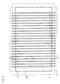
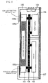
- FIG. 8 illustrates a sectional view of a plasma display device having a conventional PDP
- Fig. 9 illustrates a relationship between a light-emitting/non-light-emitting region and a bus bar region of a film-form front filter of a conventional PDP
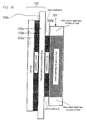
- Fig. 10 illustrates a detailed sectional view of a conventional film-form front filter.
- the PDP 101 is accommodated in a rectangular housing 106.
- a film-form front filter 102 is attached on the front face of the PDP 101.
- the PDP 101 is fixed on one face of a support substrate 104 disposed on the rear face of the PDP 101.
- a power supply circuit 105 and a circuit-mounted substrate 103 including various kinds of circuits are provided on the other face of the support substrate 104.
- the support substrate 104 is fixed to a rear panel 107, which is mounted to the housing 106.
- a fan 108 is provided on the upper part of the housing 106.
- An opening 106a corresponding to a light-emitting region of the PDP 101 is defined by a front frame 106b of the housing 106.
- the film-form front filter 102 has a rectangular shape which is somewhat larger than the PDP 101.
- the periphery of the film-form front filter 102 constitutes a bus bar region 102e.
- the bus bar region 102e is positioned at the outside of the periphery of the PDP 101 and electrically contact with a conductor (not shown) provided on the rear face of the front flame 106b of the housing 106.
- An electromagnetic wave radiated from the PDP 101 is converted into a current in the film-form front filter 102.
- noise generated by the radiation of the electromagnetic wave is reduced.
- the film-form front filter 102 is constituted by attaching an anti-reflection film (AR film) 102a as an optical property adjusting film on the front face of a transparent conductive film 102c via a transparent adhesive layer 102b.
- the anti-reflection film 102a and the transparent adhesive layer 102b do not extend to the periphery of the transparent conductive film 102c so that the periphery of the transparent conductive film 102c constitutes the bus bar region 102e as an exposed part of the conductive film.
- the transparent conductive film 102c is constructed, for example, by forming a film of ITO (indium-tin-oxide) on a substrate sheet made of PET (polyethylene terephthalate).
- An acrylic adhesive may be used for the transparent adhesive layer 102b.
- the film-form front filter 102 is attached on the front face of the PDP 101 by use of a transparent adhesive layer 102d applied on the rear face of the transparent conductive film 102c.
- the transparent adhesive layer 102d does not extend over the non-light-emitting region of the PDP 101. Therefore, the film-form front filter 102 can be detached from the non-light-emitting region and this detachable region is referred to as a repair region.
- the repair region is formed by detaching the filter 102 from the non-light-emitting region.
- discharge electrodes for example, address electrodes are found broken by a lighting test of the PDP 101 after its production, a new repair wire must be provided, which will cause complicated repair. Therefore, the conventional flat display device has a problem that its repair cannot be carried out smoothly.
- the present invention provides a front film for a flat display panel comprising a sheet body having the form of a sheet to cover a display surface of a flat display panel, the sheet body having a repair wire attached to a part thereof for repairing an electrode of the flat display panel.
- the repair wire is previously formed in the film.
- the repair wire can be carried out by recovering easily and smoothly electrical connection of the address electrode by use of the repair wire without further providing a new repair wire.
- the repair wire may be formed at a location corresponding to a non-display region of the flat display panel.
- the repair wire since the repair wire is formed at a location in the film which location corresponds to a non-display region of the flat display panel, the repair wire does not prevent display when the flat display panel is driven.
- the film of the present invention may include an electromagnetic shield layer, if necessary, and the repair wire may be formed by the same process as the electromagnetic shield layer is formed.
- the repair wire which is similar in conductivity to the electromagnetic shield layer may be formed by the same process. For this reason, production time and costs in forming the repair wire can be reduced by simplifying a process for producing the repair wire as compared with the case where the electromagnetic shield layer and the repair wire are separately formed.
- the repair wire may be formed apart from the periphery of the electromagnetic shield layer, as required.
- the electromagnetic shield layer and repair wire, which both have conductivity may be formed so as not to contact with each other. Thereby they are electrically separated, which prevents a problem caused by interference.
- the film of the present invention may be composed of at least one of an optical filter, an electromagnetic shield layer and a protective layer, if necessary.
- a flat display device includes the above-described film attached on the front face of a flat display panel with intervention of a transparent adhesive layer.
- a transparent protective board to which the above-described film is attached may be provided on the front of the flat display panel.
- the present invention may provide a sheet-form front film for a plasma display panel to be mounted on a front face of the PDP having at least one of an optical filter and an electromagnetic shield layer, wherein a repair wire is provided at a location outside a display region of the front film for repairing an electrode of the plasma display panel.
- the film may be attached on a display surface of the PDP with intervention of the transparent adhesive layer.
- Fig. 1 illustrates a front view of a PDP on which a film according to the present embodiment is formed
- Fig. 2 shows a sectional view taken along line I-I of the PDP shown in Fig. 1
- Fig. 3 illustrates a view illustrating a break in an address electrode of the PDP according to the present embodiment
- Fig. 4 shows a front view of the PDP after repair according to the present embodiment
- Fig. 5 illustrates a sectional view of a plasma display device including the PDP after repair according to the present embodiment.
- the plasma display device including a PDP 1 comprises the PDP 1, a film 2 attached on the front face thereof, a driving circuit 3 for driving the PDP 1, a rectangular housing 6 for accomodating the PDP 1, the driving circuit 3 and the like and a fixing member 4 for fixing the PDP 1, the driving circuit 3 and the like to the housing 6.
- the above PDP 1 is assumed to be a usual three-electrode discharge PDP comprising a front substrate 11 on which main electrodes (sustain electrodes) (not shown) are arranged and a rear substrate 12 on which address electrodes are arranged and including a mixed gas of neon and xenon between the front substrate 11 and the address substrate 14.
- a front substrates 11 is provided with a glass substrate as a base of the front substrate 11, a plurality of first main electrodes exclusively for a sustain discharge and a plurality of second main electrodes both for an address discharge and the sustain discharge which are arranged in pairs parallel to each other on an inside face of the glass substrate, a dielectric layer (not shown) for covering the first and the second main electrodes and a protective film (not shown) for protecting the electrodes etc. on the surface of the dielectric layers.
- the first and second main electrodes are each composed of a transparent electrode (not shown) and a bus electrode (not shown).
- the rear substrate 12 is provided with a glass substrate (not shown) as a base of the rear substrate 12, address electrodes 14 arranged on the surface of the glass substrate so as to cross with the main electrodes on the front substrate 11 when the front substrate 11 is combined with the rear substrate 12 together, a dielectric layer (not shown) for covering the address electrodes 14, barrier ribs (not shown) on the dielectric layer for partitioning a discharge space and a fluorescent layer (not shown) of RGB colors formed between the barrier ribs.
- the above film 2 includes a color adjusting layer 21 for filtering the color of light emitted by discharge gas, an infrared shield layer 22 for shielding a line spectrum in a near infrared light region radiated from the PDP 1, an electromagnetic shield layer 23 for shielding an electromagnetic wave radiated from the PDP 1 and a driving circuit 3, a repair wire 24 as a reserve wire to be used when the address electrode 14 is broken, the repair wire being provided according to the features of the present invention, an anti-reflection layer 25 for adjusting optical properties and a protective layer 26 for preventing a flow in this order from a PDP 1 side.
- the color adjusting layer 21 preferably has a property of selectively absorbing/attenuating visible light in a predetermined wavelength region and a dye filter utilizing light absorption of the dye is used therefor.
- the electromagnetic shield layer 23 is formed of a thin-film silver or a thin-film ITO by sputtering.
- the anti-reflection layer 25 is composed of a layer multicoated by vapor deposition with various kinds of thin-film metal oxides each designated optically to have a different refractive index.
- the protective layer 26 is formed by polymerizing and curing a film of acrylic resin, siloxane resin, melanin resin or the like.
- the repair wire 24 is formed of a thin-film silver by sputtering in the same manner and at the same time as the electromagnetic shield layer 23 is formed.
- the repair wire is provided in the film 2 to be attached on the display screen of the PDP 1, corresponding to a non-display region, and at the periphery of the electromagnetic shield layer 23.
- the repair wire 24 includes a connecting portion which is an exposed conductive portion for connecting to the driving circuit 3.
- the completed PDP 1 is tested on conductivity of each electrode thereof, lighting of address cells and display cells thereof and the like. If a test result shows that an address electrode 14 is broken in the PDP 1, the film 2 having the repair wire 24 is attached on the PDP 1 via an adhesive layer (not shown). If the address electrodes 14 are not broken in the PDP 1 as a result of the above lighting test of the cells, a usual film not having the repair wire 24 is attached on the PDP 1 via an adhesive layer (not shown). Only the PDP 1 on which the film 2 having the repair wire 24 is attached will be explained hereinafter.
- the broken address electrode 14 is specified by the above test.
- the address electrode 14 By connecting to the driving circuit 3 at a connection point ⁇ , the address electrode 14 allows address cells between the point ⁇ and a broken point ⁇ to be lit up, but does not allow address cells between the point ⁇ and a connection point ⁇ ' to be lit up. Therefore, the address electrode 14a is connected at the point ⁇ to the repair wire 24 via a lead line ⁇ and the address electrode 14b is connected at the point ⁇ ' to the repair wire 24 via a lead line ⁇ ' (see Figs. 4 and 5).
- the upper side of the address electrode 14 is indicated by 14a and the lower side thereof is indicated by 14b at the boundary of the broken point ⁇ .
- a voltage is applied from the driving circuit 3 to the address electrode 14 including the broken point ⁇ , from the connection point ⁇ which is one end of the address electrode 14 to the repair wire 24 via the lead line ⁇ , from the repair wire 24 to the connection point ⁇ ' which is the other end of the address electrode 14, and from the point ⁇ ' to the address electrode 14b via the lead line ⁇ '. That is, it is possible to light up the address cells between the broken point ⁇ and the connection point ⁇ ' by recovering electrical connection of the address electrode via the repair wire 24.
- the film 2 previously provided with the repair wire 24 is attached on the PDP 1, a lot of time and labor for forming a special repair wire can be omitted after attaching the film.
- the electromagnetic shield layer 23 comprising the thin film and the repair wire 24 is not conductive to each other. Thereby, the PDP 1 can be easily and, smoothly completed.
- FIG. 6 shows a view illustrating breaks in address electrodes of a PDP according to the present embodiment
- Fig. 7 shows a front view of the PDP after repair according to the present embodiment.
- the PDP 1 of the present embodiment is constructed in substantially the same manner as in the first embodiment, except that two inside and outside repair wires 241 and 242 instead of the repair wire 24 are provided at a location in the film 2 corresponding to a non-display region of the PDP 1 and at the periphery of the electromagnetic shield layer 23 as shown in Fig. 6.
- a repair work for electrodes of the PDP 1 according to the present embodiment will be explained in the case where, as shown in Fig. 6, three address electrodes 141, 142 and 143 are broken at broken points ⁇ 1, ⁇ 2 and ⁇ 3, respectively.
- the lightning test is carried out on the PDP 1 with a film 2 attached thereto via an adhesive layer (not shown) and the first broken address electrode 141 is specified by the above test.
- the address electrode 141 By connecting to a driving circuit 3 at a connection point ⁇ 1, the address electrode 141 allows address cells between the point ⁇ 1 and the broken point ⁇ 1 to be lit up, but dose not allow address cells between the point ⁇ 1 and a connection point ⁇ 1' to be lit up. Therefore, as shown in Fig.
- the first address electrode 141a is connected at the point ⁇ 1 to the inside repair wire 241 via a lead line ⁇ 1 and the first address electrode 141b is connected at the point ⁇ 1' to the inside repair wire 241 via a lead line ⁇ 1'.
- the upper side of the first address electrode 141 is indicated by 141a and the lower side thereof is indicated by 141b at the boundary of the broken point ⁇ 1.
- the second broken address electrode 142 is specified by the above test.
- the address electrode 142 allows address cells between the point ⁇ 2 and the broken point ⁇ 2 to be lit up, but does not allows address cells between the point ⁇ 2 and a connection point ⁇ 2' to be lit up. Therefore, as shown in Fig. 7, the second address electrode 142a is connected at the point ⁇ 2 to an outside repair wire 242 via a lead line ⁇ 2 and the second address electrode 142b is connected at the point ⁇ 2' to the outside repair wire 242 via a lead line ⁇ 2'.
- the upper side of the second address electrode 142 is indicated by 142a and the lower side thereof is indicated by 142b at the boundary of the broken point ⁇ 2.
- the third broken address electrode 143 is specified by the above test.
- the address electrode 143 allows address cells between the point ⁇ 3 and the broken point ⁇ 3 to be lit up, but does not allow address cells between the point ⁇ 3 and a connection point ⁇ 3' to be lit up. Therefore, as shown in Fig. 7, the third address electrode 143a is connected at the point ⁇ 3 to the outside repair wire 242 via a lead line ⁇ 3 and the third address electrode 143b is connected at the point ⁇ 3' to the outside repair wire 242 via a lead line ⁇ 3'.
- the upper side of the third address electrode 143 is indicated by 143a and the lower side thereof is indicated by 143b at the boundary of the broken point ⁇ 3.
- the inside and outside repair wires 241 and 242 are provided at the periphery of a display part of the PDP 1.
- the circular repair wire 242 is partially cut out at points ⁇ and ⁇ ', respectively.
- a voltage is applied from the driving circuit 3 to the first address electrode 141 including the broken point ⁇ 1, from the connection point ⁇ 1 which is one end of the first address electrode 141 to the inside repair wire 241 via the lead line ⁇ 1, from the inside repair wire 241 to the connection point ⁇ 1' which is the other end of the first address electrode 141 via the lead line ⁇ 1' and from the point ⁇ 1' to the first address electrode 141b.
- a voltage is applied from the driving circuit 3 to the second address electrode 142 including the broken point ⁇ 2, from the connection point ⁇ 2 which is one end of the second address electrode 142 to the outside repair wire 242 via the lead line ⁇ 2, from the outside repair wire 242 to the connection point ⁇ 2' which is the other end of the second address electrode 142 via the lead line ⁇ 2' and from. the point ⁇ 2' to the second address electrode 142b.
- a voltage is applied from the driving circuit 3 to the third address electrode 143 including the broken point ⁇ 3, from the connection point ⁇ 3 which is the one end of the third address electrode 143 to the outside repair wire 242 via the lead line ⁇ 3, from the outside repair wire 242 to the connection point ⁇ 3' which is the other end of the third address electrode 143 and from the point ⁇ 3' to the third address electrode 143b.
- the film 2 including the double repair wires since the film 2 including the double repair wires is attached, it is possible to recover electric connection and light up address cells which was not able to be lit up due to breaks even if a plurality of the address electrodes 141, 142 and 143 are broken.
- the repair wire 24 is formed outside the display region of the PDP 1.
- the repair wire 24 may be formed within the display region by forming a transparent repair wire or by changing the form of the electromagnetic shield layer 23 to use a portion thereof as the repair wire 24 or use the portion both as the electromagnetic shield layer 23 and the repair wire 24.
- the film 2 including the repair wire 24 is attached on the PDP 1 which is found to have the broken address electrodes 14.
- the films 2 with the repair wire 24 may be attached on all PDPs 1 regardless of whether or not the PDPs include broken address electrodes 14. Thus, manufacturing lines can be easily designed and operated.
- the film 2 including the number of repair wires 24 in accordance with the number of broken address electrodes is attached on the PDP 1.
- the film 2 is attached on the PDP 1 after the lighting test in the above embodiments, the film 2 including the repair wire 24 may be used for all PDPs 1 before the lighting test.
- the film 2 to be attached on the PDP 1 is composed of the color adjusting layer 21, the infrared shield layer 22, the electromagnetic shield layer 23, the repair wire 24, the anti-reflection layer 25 and the protective layer 26.
- these components are not indispensable except for the repair wire 24, and the film 2 may be composed without some of them but the repair wire 24 is essential.
- the film 2 can be constituted by adding other elements such as an impact easing layer for further protecting the panel from mechanical impact.
- the film 2 and the PDP 1 can be separated.
- the film 2 may be attached to the inside face of a transparent protective board (a transparent front cover board) which is provided at the frontmost of a plasma display.
- the repair wire 24 is formed of a thin-film silver by sputtering in the same manner and at the same time as the electromagnetic shield layer 23.
- the formation of the repair wire 24 is not particularly limited to the same manner and time as described above.
- the repair wire 24 is used for repairing the broken address electrodes, but it can also be used for repairing the main electrodes (sustain electrodes). Further, it can also be applied to panels such as LCDs, ELs, FEDs and the like in addition to PDPs.
- the present invention since the film is previously provided with the repair wire, the present invention has an effect in carrying out repair by recovering easily and smoothly electrical connection with use of the repair wire formed on the film without providing a new repair wire, for example, when the address electrodes are broken in a plasma display.
- the repair wire formed at a location in the film corresponding to a non-display region of the flat display panel does not prevent display when the flat display panel is driven. This is an effect of the present invention.
- the present invention Since the repair wire which is similar in conductivity to the electromagnetic shield layer is formed by the same process, the present invention has an effect in capable of reducing production time and costs in forming the repair wire by simplifying a process for producing the repair wire compared with the case where the electromagnetic shield layer and the repair wire are separately formed.
- the conductive electromagnetic shield layer and the conductive repair layer are formed so as not to contact with each other, they are not electrically connected and problems caused by interference can be prevented. This is another effect of the present invention.
Landscapes
- Engineering & Computer Science (AREA)
- Physics & Mathematics (AREA)
- Plasma & Fusion (AREA)
- Manufacturing & Machinery (AREA)
- Electromagnetism (AREA)
- Devices For Indicating Variable Information By Combining Individual Elements (AREA)
- Gas-Filled Discharge Tubes (AREA)
- Liquid Crystal (AREA)
Applications Claiming Priority (2)
| Application Number | Priority Date | Filing Date | Title |
|---|---|---|---|
| JP2002094830A JP4010846B2 (ja) | 2002-03-29 | 2002-03-29 | フラットディスプレイパネル用前面フィルム及びこれを用いたフラットディスプレイ装置、並びに、プラズマディスプレイパネル用前面フィルム及びこれを用いたプラズマディスプレイ装置 |
| JP2002094830 | 2002-03-29 |
Publications (2)
| Publication Number | Publication Date |
|---|---|
| EP1349189A2 true EP1349189A2 (fr) | 2003-10-01 |
| EP1349189A3 EP1349189A3 (fr) | 2008-06-25 |
Family
ID=27800542
Family Applications (1)
| Application Number | Title | Priority Date | Filing Date |
|---|---|---|---|
| EP20030251607 Withdrawn EP1349189A3 (fr) | 2002-03-29 | 2003-03-17 | Film frontal pour panneau d'affichage plat et dispositif d'affichage plat l'utilisant |
Country Status (6)
| Country | Link |
|---|---|
| US (1) | US6844684B2 (fr) |
| EP (1) | EP1349189A3 (fr) |
| JP (1) | JP4010846B2 (fr) |
| KR (1) | KR100721473B1 (fr) |
| CN (1) | CN1237497C (fr) |
| TW (1) | TW594618B (fr) |
Cited By (1)
| Publication number | Priority date | Publication date | Assignee | Title |
|---|---|---|---|---|
| US7492081B2 (en) | 2004-12-22 | 2009-02-17 | Fujitsu Hitachi Plasma Display Limited | Display panel module and method for manufacturing the same |
Families Citing this family (15)
| Publication number | Priority date | Publication date | Assignee | Title |
|---|---|---|---|---|
| US7248235B2 (en) * | 2001-09-14 | 2007-07-24 | Sharp Kabushiki Kaisha | Display, method of manufacturing the same, and method of driving the same |
| JP4010846B2 (ja) * | 2002-03-29 | 2007-11-21 | 富士通日立プラズマディスプレイ株式会社 | フラットディスプレイパネル用前面フィルム及びこれを用いたフラットディスプレイ装置、並びに、プラズマディスプレイパネル用前面フィルム及びこれを用いたプラズマディスプレイ装置 |
| KR100589370B1 (ko) * | 2003-11-26 | 2006-06-14 | 삼성에스디아이 주식회사 | 플라즈마 디스플레이 장치 |
| JP2005215554A (ja) | 2004-01-30 | 2005-08-11 | Fujitsu Hitachi Plasma Display Ltd | ディスプレイパネル装置 |
| JP2005221897A (ja) | 2004-02-06 | 2005-08-18 | Fujitsu Hitachi Plasma Display Ltd | ディスプレイパネル装置 |
| JP4625642B2 (ja) | 2004-02-19 | 2011-02-02 | 日立プラズマディスプレイ株式会社 | ディスプレイ装置 |
| JP4736373B2 (ja) * | 2004-08-03 | 2011-07-27 | 日油株式会社 | 近赤外線吸収材及びそれを用いた表示装置 |
| US7504331B2 (en) * | 2005-07-27 | 2009-03-17 | Palo Alto Research Center Incorporated | Method of fabricating self-assembled electrical interconnections |
| US7525194B2 (en) * | 2005-07-27 | 2009-04-28 | Palo Alto Research Center Incorporated | System including self-assembled interconnections |
| US7662708B2 (en) * | 2005-07-27 | 2010-02-16 | Palo Alto Research Center Incorporated | Self-assembled interconnection particles |
| KR101175728B1 (ko) * | 2006-01-20 | 2012-08-22 | 삼성전자주식회사 | 디스플레이 모듈의 전자파 차폐장치 및 그 제조방법 |
| TW200729269A (en) * | 2006-01-27 | 2007-08-01 | Marketech Int Corp | Plasma display panel and method for manufacturing the same |
| KR100820969B1 (ko) * | 2006-08-07 | 2008-04-10 | 엘지전자 주식회사 | 플라즈마 디스플레이 장치 |
| TW201216233A (en) * | 2010-10-15 | 2012-04-16 | Chunghwa Picture Tubes Ltd | Display device and repair method thereof |
| JP2013152837A (ja) * | 2012-01-25 | 2013-08-08 | Panasonic Corp | プラズマディスプレイパネル |
Family Cites Families (15)
| Publication number | Priority date | Publication date | Assignee | Title |
|---|---|---|---|---|
| US4304450A (en) * | 1979-12-17 | 1981-12-08 | International Business Machines Corporation | Repair of open circuited gas discharge display panel conductors |
| JPS599634A (ja) * | 1982-07-07 | 1984-01-19 | Seiko Epson Corp | 液晶表示装置 |
| FR2572833B1 (fr) * | 1984-11-06 | 1987-01-02 | Thomson Csf | Procede de reparation des electrodes d'un panneau d'affichage |
| JPH0766253B2 (ja) * | 1986-06-20 | 1995-07-19 | 松下電器産業株式会社 | マトリクス型画像表示装置 |
| JPH0823643B2 (ja) * | 1989-03-28 | 1996-03-06 | シャープ株式会社 | アクティブマトリクス表示装置 |
| JPH05297397A (ja) * | 1992-02-20 | 1993-11-12 | Fujitsu Ltd | 液晶表示パネルのバス配線修復方法 |
| KR0149309B1 (ko) * | 1995-09-06 | 1998-10-15 | 김광호 | 수리선을 가지고 있는 액정 표시 장치 |
| KR0169366B1 (ko) * | 1995-12-05 | 1999-03-20 | 김광호 | 액정 표시 장치용 박막 트랜지스터 기판 |
| KR100260611B1 (ko) * | 1997-04-03 | 2000-07-01 | 윤종용 | 배선을 수리하기 위한 평판 표시 장치용 기판 |
| JPH10282896A (ja) * | 1997-04-07 | 1998-10-23 | Mitsubishi Electric Corp | 表示装置 |
| KR100242943B1 (ko) * | 1997-05-30 | 2000-02-01 | 윤종용 | 수리선이 형성된 액정표시장치 |
| FR2770022B1 (fr) * | 1997-10-20 | 1999-12-03 | Itt Mfg Enterprises Inc | Commutateur electrique multiple a levier unique d'actionnement |
| US20020050783A1 (en) * | 2000-06-01 | 2002-05-02 | Tadahiko Kubota | Electromagnetic-wave-shielding film, production method thereof and image display device using the same |
| JP3557154B2 (ja) | 2000-06-02 | 2004-08-25 | 三洋電機株式会社 | プラズマディスプレイ装置 |
| JP4010846B2 (ja) * | 2002-03-29 | 2007-11-21 | 富士通日立プラズマディスプレイ株式会社 | フラットディスプレイパネル用前面フィルム及びこれを用いたフラットディスプレイ装置、並びに、プラズマディスプレイパネル用前面フィルム及びこれを用いたプラズマディスプレイ装置 |
-
2002
- 2002-03-29 JP JP2002094830A patent/JP4010846B2/ja not_active Expired - Fee Related
-
2003
- 2003-03-17 EP EP20030251607 patent/EP1349189A3/fr not_active Withdrawn
- 2003-03-17 US US10/388,554 patent/US6844684B2/en not_active Expired - Fee Related
- 2003-03-18 TW TW92105955A patent/TW594618B/zh not_active IP Right Cessation
- 2003-03-28 CN CNB031083552A patent/CN1237497C/zh not_active Expired - Fee Related
- 2003-03-28 KR KR20030019572A patent/KR100721473B1/ko not_active Expired - Fee Related
Cited By (2)
| Publication number | Priority date | Publication date | Assignee | Title |
|---|---|---|---|---|
| US7492081B2 (en) | 2004-12-22 | 2009-02-17 | Fujitsu Hitachi Plasma Display Limited | Display panel module and method for manufacturing the same |
| EP1677334A3 (fr) * | 2004-12-22 | 2009-02-25 | Hitachi Plasma Display Limited | Module de panneau d'affichage et son procédé de fabrication |
Also Published As
| Publication number | Publication date |
|---|---|
| TW594618B (en) | 2004-06-21 |
| CN1237497C (zh) | 2006-01-18 |
| US20030184225A1 (en) | 2003-10-02 |
| TW200305121A (en) | 2003-10-16 |
| EP1349189A3 (fr) | 2008-06-25 |
| CN1448899A (zh) | 2003-10-15 |
| KR20030078775A (ko) | 2003-10-08 |
| US6844684B2 (en) | 2005-01-18 |
| JP4010846B2 (ja) | 2007-11-21 |
| JP2003295779A (ja) | 2003-10-15 |
| KR100721473B1 (ko) | 2007-05-23 |
Similar Documents
| Publication | Publication Date | Title |
|---|---|---|
| EP1349189A2 (fr) | Film frontal pour panneau d'affichage plat et dispositif d'affichage plat l'utilisant | |
| US7242136B2 (en) | Front filter, and plasma display apparatus having the same | |
| JP2917279B2 (ja) | ガス放電パネル | |
| KR100623845B1 (ko) | 백라이트 어셈블리 및 이를 구비한 액정표시장치 | |
| US20060158116A1 (en) | Plasma display panel having electromagnetic wave shielding layer | |
| US7687995B2 (en) | Display apparatus | |
| JP2001343898A (ja) | プラズマディスプレイ装置 | |
| US20040155584A1 (en) | Plasma display panel | |
| US20020033669A1 (en) | Plasma display panel and method of manufacturing the same | |
| JP2007148275A (ja) | プラズマディスプレイパネルにおける光学フィルタの接地構造 | |
| KR100701943B1 (ko) | 플라즈마 디스플레이 패널 및 그 제조 방법 | |
| JP2005017534A (ja) | プラズマ表示装置 | |
| CN113268165B (zh) | 触控模组、显示模组及显示装置 | |
| US7605538B2 (en) | Plasma display panel | |
| CN214896564U (zh) | 电容式触摸屏结构、显示器、终端和轨道交通工具 | |
| US7411346B2 (en) | Plasma display panel having multiple substrate parts | |
| KR19990070801A (ko) | 플라즈마 표시장치용 전면필터 | |
| KR20070054850A (ko) | 플라즈마 디스플레이 패널용 필름형 전면 필터 및 그의제조방법 | |
| KR100824837B1 (ko) | 플라즈마 디스플레이 패널 | |
| CN101655573A (zh) | 用于等离子体显示面板的滤光器及等离子体显示装置 | |
| JP2005121703A (ja) | プラズマディスプレイ装置 | |
| KR100573157B1 (ko) | 플라즈마 디스플레이 패널 | |
| TW425535B (en) | Plasma display panel using light shading layer to control the color temperature | |
| KR100776506B1 (ko) | 방열효율이 향상된 플라즈마 디스플레이 장치 | |
| JP2004093860A (ja) | プラズマディスプレイ装置 |
Legal Events
| Date | Code | Title | Description |
|---|---|---|---|
| PUAI | Public reference made under article 153(3) epc to a published international application that has entered the european phase |
Free format text: ORIGINAL CODE: 0009012 |
|
| AK | Designated contracting states |
Kind code of ref document: A2 Designated state(s): AT BE BG CH CY CZ DE DK EE ES FI FR GB GR HU IE IT LI LU MC NL PT RO SE SI SK TR |
|
| AX | Request for extension of the european patent |
Extension state: AL LT LV MK |
|
| PUAL | Search report despatched |
Free format text: ORIGINAL CODE: 0009013 |
|
| AK | Designated contracting states |
Kind code of ref document: A3 Designated state(s): AT BE BG CH CY CZ DE DK EE ES FI FR GB GR HU IE IT LI LU MC NL PT RO SE SI SK TR |
|
| AX | Request for extension of the european patent |
Extension state: AL LT LV MK |
|
| AKX | Designation fees paid | ||
| REG | Reference to a national code |
Ref country code: DE Ref legal event code: 8566 |
|
| STAA | Information on the status of an ep patent application or granted ep patent |
Free format text: STATUS: THE APPLICATION IS DEEMED TO BE WITHDRAWN |
|
| 18D | Application deemed to be withdrawn |
Effective date: 20080626 |