EP1351302B2 - Leistungshalbleitermodul - Google Patents
Leistungshalbleitermodul Download PDFInfo
- Publication number
- EP1351302B2 EP1351302B2 EP03005024.9A EP03005024A EP1351302B2 EP 1351302 B2 EP1351302 B2 EP 1351302B2 EP 03005024 A EP03005024 A EP 03005024A EP 1351302 B2 EP1351302 B2 EP 1351302B2
- Authority
- EP
- European Patent Office
- Prior art keywords
- power semiconductor
- pressure
- substrate
- contact
- semiconductor module
- Prior art date
- Legal status (The legal status is an assumption and is not a legal conclusion. Google has not performed a legal analysis and makes no representation as to the accuracy of the status listed.)
- Expired - Lifetime
Links
Images


Classifications
-
- H—ELECTRICITY
- H05—ELECTRIC TECHNIQUES NOT OTHERWISE PROVIDED FOR
- H05K—PRINTED CIRCUITS; CASINGS OR CONSTRUCTIONAL DETAILS OF ELECTRIC APPARATUS; MANUFACTURE OF ASSEMBLAGES OF ELECTRICAL COMPONENTS
- H05K1/00—Printed circuits
- H05K1/18—Printed circuits structurally associated with non-printed electric components
- H05K1/181—Printed circuits structurally associated with non-printed electric components associated with surface mounted components
-
- H—ELECTRICITY
- H10—SEMICONDUCTOR DEVICES; ELECTRIC SOLID-STATE DEVICES NOT OTHERWISE PROVIDED FOR
- H10W—GENERIC PACKAGES, INTERCONNECTIONS, CONNECTORS OR OTHER CONSTRUCTIONAL DETAILS OF DEVICES COVERED BY CLASS H10
- H10W72/00—Interconnections or connectors in packages
-
- H—ELECTRICITY
- H10—SEMICONDUCTOR DEVICES; ELECTRIC SOLID-STATE DEVICES NOT OTHERWISE PROVIDED FOR
- H10W—GENERIC PACKAGES, INTERCONNECTIONS, CONNECTORS OR OTHER CONSTRUCTIONAL DETAILS OF DEVICES COVERED BY CLASS H10
- H10W90/00—Package configurations
-
- H—ELECTRICITY
- H05—ELECTRIC TECHNIQUES NOT OTHERWISE PROVIDED FOR
- H05K—PRINTED CIRCUITS; CASINGS OR CONSTRUCTIONAL DETAILS OF ELECTRIC APPARATUS; MANUFACTURE OF ASSEMBLAGES OF ELECTRICAL COMPONENTS
- H05K1/00—Printed circuits
- H05K1/02—Details
- H05K1/03—Use of materials for the substrate
- H05K1/0306—Inorganic insulating substrates, e.g. ceramic, glass
-
- H—ELECTRICITY
- H05—ELECTRIC TECHNIQUES NOT OTHERWISE PROVIDED FOR
- H05K—PRINTED CIRCUITS; CASINGS OR CONSTRUCTIONAL DETAILS OF ELECTRIC APPARATUS; MANUFACTURE OF ASSEMBLAGES OF ELECTRICAL COMPONENTS
- H05K2201/00—Indexing scheme relating to printed circuits covered by H05K1/00
- H05K2201/10—Details of components or other objects attached to or integrated in a printed circuit board
- H05K2201/10007—Types of components
- H05K2201/10166—Transistor
-
- H—ELECTRICITY
- H05—ELECTRIC TECHNIQUES NOT OTHERWISE PROVIDED FOR
- H05K—PRINTED CIRCUITS; CASINGS OR CONSTRUCTIONAL DETAILS OF ELECTRIC APPARATUS; MANUFACTURE OF ASSEMBLAGES OF ELECTRICAL COMPONENTS
- H05K2201/00—Indexing scheme relating to printed circuits covered by H05K1/00
- H05K2201/10—Details of components or other objects attached to or integrated in a printed circuit board
- H05K2201/10227—Other objects, e.g. metallic pieces
- H05K2201/1031—Surface mounted metallic connector elements
- H05K2201/10318—Surface mounted metallic pins
-
- H—ELECTRICITY
- H05—ELECTRIC TECHNIQUES NOT OTHERWISE PROVIDED FOR
- H05K—PRINTED CIRCUITS; CASINGS OR CONSTRUCTIONAL DETAILS OF ELECTRIC APPARATUS; MANUFACTURE OF ASSEMBLAGES OF ELECTRICAL COMPONENTS
- H05K3/00—Apparatus or processes for manufacturing printed circuits
- H05K3/0058—Laminating printed circuit boards onto other substrates, e.g. metallic substrates
- H05K3/0061—Laminating printed circuit boards onto other substrates, e.g. metallic substrates onto a metallic substrate, e.g. a heat sink
-
- H—ELECTRICITY
- H05—ELECTRIC TECHNIQUES NOT OTHERWISE PROVIDED FOR
- H05K—PRINTED CIRCUITS; CASINGS OR CONSTRUCTIONAL DETAILS OF ELECTRIC APPARATUS; MANUFACTURE OF ASSEMBLAGES OF ELECTRICAL COMPONENTS
- H05K3/00—Apparatus or processes for manufacturing printed circuits
- H05K3/30—Assembling printed circuits with electric components, e.g. with resistors
- H05K3/32—Assembling printed circuits with electric components, e.g. with resistors electrically connecting electric components or wires to printed circuits
- H05K3/325—Assembling printed circuits with electric components, e.g. with resistors electrically connecting electric components or wires to printed circuits by abutting or pinching; Mechanical auxiliary parts therefor
-
- H—ELECTRICITY
- H10—SEMICONDUCTOR DEVICES; ELECTRIC SOLID-STATE DEVICES NOT OTHERWISE PROVIDED FOR
- H10W—GENERIC PACKAGES, INTERCONNECTIONS, CONNECTORS OR OTHER CONSTRUCTIONAL DETAILS OF DEVICES COVERED BY CLASS H10
- H10W72/00—Interconnections or connectors in packages
- H10W72/50—Bond wires
- H10W72/531—Shapes of wire connectors
- H10W72/5363—Shapes of wire connectors the connected ends being wedge-shaped
-
- H—ELECTRICITY
- H10—SEMICONDUCTOR DEVICES; ELECTRIC SOLID-STATE DEVICES NOT OTHERWISE PROVIDED FOR
- H10W—GENERIC PACKAGES, INTERCONNECTIONS, CONNECTORS OR OTHER CONSTRUCTIONAL DETAILS OF DEVICES COVERED BY CLASS H10
- H10W72/00—Interconnections or connectors in packages
- H10W72/50—Bond wires
- H10W72/541—Dispositions of bond wires
- H10W72/5438—Dispositions of bond wires the bond wires having multiple connections on the same bond pad
-
- H—ELECTRICITY
- H10—SEMICONDUCTOR DEVICES; ELECTRIC SOLID-STATE DEVICES NOT OTHERWISE PROVIDED FOR
- H10W—GENERIC PACKAGES, INTERCONNECTIONS, CONNECTORS OR OTHER CONSTRUCTIONAL DETAILS OF DEVICES COVERED BY CLASS H10
- H10W90/00—Package configurations
- H10W90/701—Package configurations characterised by the relative positions of pads or connectors relative to package parts
- H10W90/751—Package configurations characterised by the relative positions of pads or connectors relative to package parts of bond wires
- H10W90/754—Package configurations characterised by the relative positions of pads or connectors relative to package parts of bond wires between a chip and a stacked insulating package substrate, interposer or RDL
-
- Y—GENERAL TAGGING OF NEW TECHNOLOGICAL DEVELOPMENTS; GENERAL TAGGING OF CROSS-SECTIONAL TECHNOLOGIES SPANNING OVER SEVERAL SECTIONS OF THE IPC; TECHNICAL SUBJECTS COVERED BY FORMER USPC CROSS-REFERENCE ART COLLECTIONS [XRACs] AND DIGESTS
- Y02—TECHNOLOGIES OR APPLICATIONS FOR MITIGATION OR ADAPTATION AGAINST CLIMATE CHANGE
- Y02P—CLIMATE CHANGE MITIGATION TECHNOLOGIES IN THE PRODUCTION OR PROCESSING OF GOODS
- Y02P70/00—Climate change mitigation technologies in the production process for final industrial or consumer products
- Y02P70/50—Manufacturing or production processes characterised by the final manufactured product
Definitions
- the invention describes a power semiconductor module with active and / or passive components, in particular a power converter module.
- Such power semiconductor modules are known several times from the literature. When increasing the performance, the reliability as well as the service life with simultaneously reduced production costs, changed methods of the construction technologies for the individual components are a mandatory requirement.
- pressure build-up in such pressure-contacted power semiconductor modules is achieved by means of a mechanically stable pressure plate.
- the power semiconductor modules after DE 42 37 632 A1 or DE 199 03 875 A1 adheres to the disadvantage that, as is common in modern modules, a plurality of power semiconductor devices must be contacted with each other and / or with the substrate. Technically, this is realized by means of a plurality of individual wire bonds. Usually, up to 10 bond connections per component are usual here. Since these bonds are made in series, their manufacture requires a considerable amount of time and thus also causes a significant cost share in module production.
- a housing for hopped power semiconductor components wherein a plurality of these power semiconductor components are arranged in the housing.
- the housing of the power semiconductor components are pressed elastically by means of a common cover on a base.
- a semiconductor device having a thinned power semiconductor device arranged on a substrate is known.
- contact elements for external contacting are further arranged by way of example with a circuit board.
- the object of the present invention is to present a power semiconductor module in which at least partially bond connections for the electrical connection of the semiconductor components to the contact surfaces of the substrate can be dispensed with.
- the basic inventive idea is to replace at least one unhoused, chip-shaped power semiconductor component with a housed power semiconductor component.
- Blocked power semiconductor components according to the prior art have the same electrical parameters as the power semiconductor components used in power semiconductor modules.
- Chimney variants however, have the advantage compared to the unhoused that you have led out of the housing contact elements with which can produce the same electrical contacts, as they are made in the prior art by means of Drahtbonditatien.
- the gehausten power semiconductor devices can be as well as the uncaused connect by means of diverse bonding techniques with the substrate.
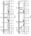
- Fig. 1 shows a power semiconductor module on a heat sink (10) according to the prior art, wherein the power semiconductor module consists of a substrate (20) with a first heat sink facing flat metallic lamination (210), a second circuitally structured structured metallic lamination (220). Unheaten chip-shaped power semiconductor components (30) are arranged on this second metallic lamination and electrically conductively connected thereto. This is done by various joining techniques, the most commonly used is the solder joint, but also adhesive bonds are known by means of conductive adhesive. Further electrical connections of the side of the power semiconductor components (30) facing away from the substrate are usually produced according to the prior art by means of wire bond connections (310). For electrical insulation of the individual components, a potting compound (90) is introduced into the housing (60). Furthermore, electrical contacts serve as main (70) and auxiliary terminals (80) connecting the substrate to external terminals. On the substrate further components such as exemplary sensors (50) may be arranged.
- Fig. 2 shows a power semiconductor module, wherein individual chip-shaped ungehauste power semiconductor devices (30) are replaced by hopped power semiconductor devices (40). These components are connected to the second metallic lamination (220) of the substrate by means of soldered connection or by means of a bonding technique with thermally conductive adhesive. It is important in this connection that the heat transfer from the power semiconductor component (40) to the heat sink, the cooling component (10), has a dimension comparable to the construction technique according to the prior art. This is exemplified by the use of known gehauster semiconductor devices (40) guaranteed in the "TO" housing with integrated heat spread.
- the contact elements (410) of the thinned power semiconductor device (40) are connected by solder joints to the corresponding contact surfaces, parts of the metallic lamination (220) of the substrate. All other components of the power semiconductor module according to the prior art (see. Fig. 1 ), such as sensors (50) and connection elements (70 and 80) can also be found here.
- Fig. 3 shows a power semiconductor module with pressure contact.
- a pressure contact according to the prior art is shown, by means of individual pressure pieces (620) of a separate cover (610) as part of the housing (60) press the substrate (20) on the cooling member and thus a very effective heat transfer between the components of the Ensure power semiconductor module and the cooling component.
- This printing device is extended by pressure pieces (630) for pressure contacting of the thinned power semiconductor components (40a).
- a cohesive connection such as soldering
- a heat-conducting medium may additionally be arranged.
- Fig. 4 shows an embodiment of a semiconductor module with pressure contact without potting compound.
- the pressure contact is off Fig. 3 extended by pressure on the contact elements (410a) of the power semiconductor device (40b) by means of a pressure piece (640) is introduced.
- This makes it possible to dispense with a soldering or adhesive contacting of this contact element (410a).
- An electrically conductive contact is thus produced between the contact elements of the power semiconductor component and the corresponding contact surface (220) of the substrate.
- both the power semiconductor component (40c) and its contact elements are pressed onto the substrate by means of suitable pressure pieces.
- both the thermally conductive transition to the heat dissipation and the electrically conductive transition to the electrical contact can be made waiving solder joints.
- the printing device can be further supplemented by an elastic cushion element (660) according to the prior art.
- the pressure of the pressure piece (650) is then not directly introduced to the power semiconductor component (40d), but instead to a permanently elastic pressure pad (660), which in turn transfers the pressure to the power semiconductor component (40d).
- the pressure pad may be configured to cover one or more power semiconductor devices and transmit pressure thereon.
- Fig. 5 shows an inventive embodiment of a power semiconductor module after Fig. 3 ,
- other types of power semiconductor device (40e) are arranged on the substrate, in that the contact elements (420a and 420b) are connected to the respectively contact surfaces (220) of the substrate (20) that are suitable for the circuit.
- the abovementioned possibilities for thermal and electrical contacting offer themselves.
- the power semiconductor component (40e) is contacted by material connection, for example a solder connection, while the power semiconductor component (40f) is contacted thermally and electrically by means of pressure contact with pressure pieces (630).
Landscapes
- Engineering & Computer Science (AREA)
- Microelectronics & Electronic Packaging (AREA)
- Cooling Or The Like Of Semiconductors Or Solid State Devices (AREA)
- Inverter Devices (AREA)
Description
- Die Erfindung beschreibt ein Leistungshalbleitermodul mit aktiven und / oder passiven Bauelementen, insbesondere ein Stromrichtermodul. Derartige Leistungshalbleitermodule sind mehrfach aus der Literatur bekannt. Bei der Erhöhung der Leistungsfähigkeit, der Zuverlässigkeit sowie der Lebensdauer bei gleichzeitig verringerten Herstellungskosten sind veränderte Methoden der Aufbautechnologien für die einzelnen Bestandteile eine zwingende Voraussetzung.
- Moderne Leistungshalbleitermodule, die Ausgangspunkt dieser Erfindung sind, sind grundplattenlose Module, wie beispielhaft in der
DE 199 03 875 A1 beschrieben, bestehend aus - einem Gehäuse;
- einem keramischen Substrat mit darauf angeordneten schaltungsgerecht ausgeführten metallischen Kaschierungen, wie sie z.B. nach dem DCB- (direct copper bonding) Verfahren hergestellt werden;
- auf diesem Substrat mittels Löttechnik stoffschlüssig aufgebrachten Bauelementen, wie beispielhaft Dioden, Transistoren, Widerständen oder Sensoren;
- Bondverbindungen zur Verbindung der strukturierten Seite der chipförmigen, ungehausten Leistungshalbleiterbauelemente mit weiteren Bauelementen und/oder dem Substrat und / oder nach außen führenden Anschlusselementen.
- Einer vorzugsweise aus Silikonkautschuk bestehenden Vergussmasse zur Isolation der einzelnen Bauelemente zueinander.
- Es hat sich gezeigt, dass sich insbesondere großflächige Lötverbindungen zu einem Kühlbauteil nur sehr schwer qualitätsgerecht beherrschen lassen, worunter die Zuverlässigkeit sowie die Lebensdauer der Leistungshalbleitermodule leiden. Sehr vorteilhaft hat daher sich für derartige Leistungshalbleitermodule die Aufbautechnologie mit Druckkontakt zur thermisch leitenden Verbindung des Moduls mit einem Kühlbauteil erwiesen.
- Der Druckaufbau in derartigen druckkontaktierten Leistungshalbleitermodulen wird mittels einer mechanisch stabilen Druckplatte erzielt. Je nach weiterer Ausgestaltung kann der erzeugte Druck direkt mittels speziell ausgestalteter Druckstücke der Druckplatte, wie beispielhaft in der
DE 42 37 632 A1 gezeigt, oder mittels eines elastischen Druckspeichers nach derDE 199 03 875 A1 , auf das Substrat übertragen werden. - Den Leistungshalbleitermodulen nach
DE 42 37 632 A1 oderDE 199 03 875 A1 haftet der Nachteil an, dass, wie bei modernen Modulen üblich, eine Vielzahl von Leistungshalbleiterbauelementen miteinander und / oder mit dem Substrat kontaktiert werden müssen. Technisch wird dies mittels einer Vielzahl einzelner Drahtbondverbindungen realisiert. Üblich sind hier durchaus bis zu 10 Bondverbindungen pro Bauelement. Da diese Bondverbindungen seriell hergestellt werden, erfordert ihre Herstellung einen erheblichen Zeitaufwand und verursacht damit auch einen wesentlichen Kostenanteil an der Modulherstellung. - Aus der
EP 0 625 871 A1 ist weiterhin ein Gehäuse für gehauste Leistungshalbleiterbauelemente bekannt, wobei eine Mehrzahl dieser Leistungshalbleiterbauelemente in dem Gehäuse angeordnet sind. Die Gehäuse der Leistungshalbleiterbauelemente werden hierbei elastisch mittels eines gemeinsamen Deckels auf eine Grundfläche gedrückt. - Aus der
DE 36 28 556 C1 ist eine Halbleiteranordnung mit einem gehausten Leistungshalbleiterbauelement bekannt, das auf einem Substrat angeordnet ist. Auf diesem Substrat sind weiterhin Kontaktelemente zur externen Kontaktierung beispielhaft mit einer Leiterplatte angeordnet. - Aus der
DE 195 29 237 C1 ist eine Schaltungsanordnung der Halbleiterelektronik mit großer Leistungsdichte bekannt. Auf der Grundlage eines Druckkontaktaufbaus wird durch zusätzliche Maßnahmen die Lebensdauer der Bondverbindungen erhöht, wodurch die Zuverlässigkeit der gesamten Anordnung vergrößert wird. Die erhöhte Qualität der Bondverbindungen wird durch einen Aufbau mit Druckkissen erreicht. Die Druckkissen sind erfindungsgemäß so gestaltet, dass die gebondeten Verbindungsdrähte der internen Schaltungsverdrahtung gegen die Bondkontaktflächen gedrückt werden. - Die vorliegende Erfindung hat die Aufgabe ein Leistungshalbleitermodul vorzustellen, bei dem zumindest teilweise auf Bondverbindungen zur elektrischen Verbindung der Halbleiterbauelemente mit den Kontaktflächen des Substrats verzichtet werden kann.
- Die Aufgabe wird gelöst durch die Maßnahmen des Anspruchs 1. Weitere vorteilhafte Ausgestaltungen sind in den Unteransprüchen genannt.
- Der grundlegende erfinderische Gedanke liegt darin zumindest ein ungehaustes, chipförmiges Leistungshalbleiterbauelement durch ein gehaustes Leistungshalbleiterbauelement zu ersetzen. Gehauste Leistungshalbleiterbauelemente nach dem Stand der Technik weisen die gleichen elektrischen Parameter auf wie die in Leistungshalbleitermodulen eingesetzten Leistungshalbleiterbauelemente. Gehauste Varianten weisen allerdings gegenüber den ungehausten den Vorteil auf, dass Sie über aus dem Gehäuse herausgeführte Kontaktelemente verfügen, mit denen sich die gleichen elektrischen Kontakte herstellen lassen, wie sie nach dem Stand der Technik mittels der Drahtbondverbindungen hergestellt werden. Die gehausten Leistungshalbleiterbauelemente lassen sich ebenso wie die ungehausten mittels vielfältiger Verbindungstechniken mit dem Substrat verbinden.
- Spezielle Ausgestaltungen erfinderischer Leistungshalbleitermodule werden anhand der
Fig. 1 bis 5 näher erläutert. -
Fig. 1 zeigt ein Leistungshalbleitermodul nach dem Stand der Technik -
Fig. 2 zeigt eine Abwandlung eines Leistungshalbleitermoduls gemäßFig. 1 . -
Fig. 3 zeigt eine weitere Abwandlung eines Leistungshalbleitermoduls gemäßFig. 1 mit Druckkontaktierung. -
Fig. 4 zeigt eine Ausgestaltung eines Halbleitermoduls mit Druckkontaktierung ohne Vergussmasse. -
Fig. 5 zeigt eine erfinderische Ausgestaltung eines Halbleitermoduls nachFig. 3 -
Fig. 1 zeigt ein Leistungshalbleitermodul auf einem Kühlkörper (10) nach dem Stand der Technik, wobei das Leistungshalbleitermodul besteht aus einem Substrat (20) mit einer ersten dem Kühlkörper zugewandten flächigen metallischen Kaschierung (210), einer zweiten schaltungsgerecht strukturierten metallischen Kaschierung (220). Auf dieser zweiten metallischen Kaschierung sind ungehauste chipförmige Leistungshalbleiterbauelemente (30) angeordnet und elektrisch leitend mit dieser verbunden. Hierzu dienen verschiedenen Verbindungstechniken, die am häufigsten eingesetzte ist die Lötverbindung, allerdings sind auch Klebeverbindungen mittels leitfähiger Kleber bekannt. Weitere elektrische Verbindungen der dem Substrat abgewandten Seite der Leistungshalbleiterbauelemente (30) werden nach dem Stand der Technik meist mittels Drahtbondverbindungen (310) hergestellt. Zur elektrischen Isolierung der einzelnen Bauelemente ist in das Gehäuse (60) noch eine Vergussmasse (90) eingebracht. Weiterhin dienen elektrische Kontaktierungen als Haupt-(70) und Hilfsanschlüsse (80), die das Substrat mit externen Anschlüssen verbinden. Auf dem Substrat können weitere Bauelemente wie beispielhaft Sensoren (50) angeordnet sein. -
Fig. 2 zeigt ein Leistungshalbleitermodul, wobei einzelne chipförmige ungehauste Leistungshalbleiterbauelemente (30) durch gehauste Leistungshalbleiterbauelemente (40) ersetzt sind. Diese Bauelemente sind mit der zweiten metallischen Kaschierung (220) des Substrates mittels Lötverbindung oder mittels einer Klebetechnik mit thermisch leitfähigem Kleber verbunden. Wichtig ist hierbei, dass der Wärmeübergang vom Leistungshalbleiterbauelement (40) zur Wärmesenke, dem Kühlbauteil (10), ein der Aufbautechnik nach dem Stand der Technik vergleichbares Maß aufweist. Dies ist beispielhaft durch den Einsatz bekannter gehauster Halbleiterbauelemente (40) im "TO-" Gehäuse mit integrierter Wärmespreizung gewährleistet. Die Kontaktelemente (410) des gehausten Leistungshalbleiterbauelements (40) werden durch Lötverbindungen mit den entsprechenden Kontaktflächen, Teilen der metallischen Kaschierung (220) des Substrates, verbundenen. Alle weiteren Komponenten des Leistungshalbleitermoduls nach dem Stand der Technik (vgl.Fig. 1 ), wie Sensoren (50) und Anschlusselemente (70 und 80) finden sich hier ebenfalls. -
Fig. 3 zeigt ein Leistungshalbleitermodul mit Druckkontaktierung. Hierbei wird eine Druckkontaktierung nach dem Stand der Technik gezeigt, die mittels einzelner Druckstücke (620) eines separaten Deckels (610) als Teil des Gehäuses (60) das Substrat (20) auf das Kühlbauteil drücken und somit einen sehr wirkungsvollen Wärmeübergang zwischen den Bauelementen des Leistungshalbleitermoduls und dem Kühlbauteil gewährleisten. Diese Druckeinrichtung ist erweitert um Druckstücke (630) zur Druckkontaktierung der gehausten Leistungshalbleiterbauelemente (40a). Somit kann auf eine stoffschlüssige Verbindung, wie eine Lötung, verzichtet werden, um einen thermischen leitenden Kontakt zur Wärmeabführung des Leistungshalbleiterbauelements auf das Substrat bzw. das Kühlbauteil zu ermöglichen. Zwischen Leistungshalbleiterbauelement (40) und Substrat (20), bzw. Kontaktfläche (220), kann zusätzlich ein wärmeleitendes Medium angeordnet sein. -
Fig. 4 zeigt eine Ausgestaltung eines Halbleitermoduls mit Druckkontaktierung ohne Vergussmasse. Hierbei wird die Druckkontaktierung ausFig. 3 erweitert, indem auch auf die Kontaktelemente (410a) des Leistungshalbleiterbauelements (40b) mittels eines Druckstücks (640) Druck eingeleitet wird. Hierdurch kann auf eine Löt- oder Klebekontaktierung dieses Kontaktelements (410a) verzichtet werden. Es wird so ein elektrisch leitender Kontakt zwischen den Kontaktelementen des Leistungshalbleiterbauelements und der entsprechenden Kontaktfläche (220) des Substrats hergestellt. Vorteilhafterweise werden sowohl das Leistungshalbleiterbauelement (40c) als auch dessen Kontaktelemente mittels geeigneter Druckstücke auf das Substrat gedrückt. Somit kann sowohl der thermisch leitende Übergang zur Wärmeabführung als auch der elektrisch leitende Übergang zur elektrischen Kontaktierung unter Verzicht auf Lötverbindungen hergestellt werden. Die Druckeinrichtung kann weiterhin durch ein elastisches Kissenelement (660) nach dem Stand der Technik ergänzt werden. Hierbei wird dann der Druck des Druckstücks (650) nicht direkt auf das Leistungshalbleiterbauelement (40d) eingeleitet, sondern auf ein dauerelastisches Druckkissen (660), welches seinerseits den Druck auf das Leistungshalbleiterbauelement (40d) überträgt. Das Druckkissen kann derart ausgestaltet sein, dass es eines oder mehrere Leistungshalbleiterbauelemente überdeckt und darauf Druck überträgt. -
Fig. 5 zeigt eine erfinderische Ausgestaltung eines Leistungshalbleitermoduls nachFig. 3 . Hier werden andere Bauformen des Leistungshalbleiterbauelements (40e) derart auf dem Substrat angeordnet, dass die Kontaktelemente (420a und 420b) mit den jeweils schaltungsgerechten Kontaktflächen (220) des Substrates (20) verbunden werden. Auch für derartige Leistungshalbleiterbauelemente (40e, 40f) bieten sich die bereits oben genannten Möglichkeiten zur thermischen und elektrischen Kontaktierung an. Das Leistungshalbleiterbauelement (40e) wird per stoffschlüssiger Verbindung, beispielhaft einer Lötverbindung kontaktiert, während das Leistungshalbleiterbauelement (40f) mittels einer Druckkontaktierung mit Druckstücken (630) thermisch und elektrisch kontaktiert wird. - Der Einsatz gehauster Leistungshalbleiterbauelemente in erfinderischen Leistungshalbleitermodulen weist folgenden Vorteile gegenüber dem Stand der Technik auf:
- Die Herstellung eines Leistungshalbleitermoduls wird vereinfacht, da keine oder weniger mechanisch empfindliche ungehauste Leistungshalbleiterbauelemente verwendet werden.
- Die Herstellung eines erfinderischen Leistungshalbleitermoduls kann mit den gleichen Werkzeuge erfolgen wie sie beim Stand der Technik üblich sind.
- Die Herstellung eines Leistungshalbleitermoduls wird beschleunigt, da auf aufwändige Drahtbondverbindungen zumindest zum Teil verzichtet werden kann.
- Das Leistungshalbleitermodul wird bereits in einem früheren Stadium seiner Herstellung testfähig, da die Isolierung der Bauelemente durch ihr Gehäuse sichergestellt ist und nicht erst durch das Einbringen einer Vergussmasse erreicht wird.
- Die gehausten Leistungshalbleiterbauelemente sind direkt einer Druckkontaktierung zugänglich, da ihre Gehäuse selbst mit Druck beaufschlagt werden können.
- Auf den Einsatz von Vergussmassen kann verzichtet werden, oder es kann deren Einsatz zumindest verringert werden.
- Die Leistungshalbleitermodule werden einer Reparatur zugänglich, da einzelne nicht mit auf das Substrat gelötete defekte Leistungshalbleiterbauelemente ersetzt werden können.
-
- 10
- Kühlbauteil
- 20
- Substrat
- 210
- erste metallische Kaschierung des Substrats 20
- 220
- zweite metallische Kaschierung des Substrats 20
- 30
- ungehaustes Leistungshalbleiterbauelement
- 310
- Drahtbondverbindungen
- 40
- gehaustes Leistungshalbleiterbauelement
- 410
- Kontaktelement eines Leistungshalbleiterbauelements 40
- 420
- Kontaktelement eines Leistungshalbleiterbauelements 40
- 50
- Sensor
- 60
- Gehäuse
- 610
- Deckel des Gehäuses 60
- 620
- Druckstück zum Druck auf das Substrat 20
- 630
- Druckstück zum Druck auf das Leistungshalbleiterbauelement 40
- 640
- Druckstück zum Druck auf Kontaktelemente 410
- 650
- Druckstück zum Druck auf ein Kissenelement 660
- 660
- Kissenelement
- 70
- Anschlusselement
- 80
- Anschlusselement
- 90
- Vergussmasse
Claims (3)
- Leistungshalbleitermodul, zur Druckkontaktierung mit einem Kühlbauteil (10), bestehend aus einem Gehäuse (60), mindestens einem Substrat (20), darauf schaltungsgerecht angeordneten strukturierten und elektrisch leitenden Kontaktflächen (220), mindestens einem darauf angeordneten gehausten Leistungshalbleiterbauelement (40 b/c, 40 e/f), mit Kontaktelementen (410a, 420 a/b), wobei diese Kontaktelemente (410a, 420 a/b) mit mindestens einer der Kontaktflächen (220) verbunden sind, sowie Anschlusselementen (70, 80) zur elektrischen Kontaktierung des Leitungshalbleitermoduls wobei
das Gehäuse (60) einen Deckel (610) zur Druckkontaktierung, mit oder ohne Druck speicherndes elastisches Kissenelement, aufweist und wobei der Druck über Druckstücke (640) auf die Kontaktelemente (410a, 420 a/b) des Leistungshalbleiterbauelements (40 b/c, 40 e/f) eingeleitet wird wodurch ein elektrisch leitender Kontakt zwischen den Kontaktelementen (10, 410a, 420 a/b) des Leistungshalbleiterbauelements (40 b/c, 40 e/f) und der entsprechenden Kontaktfläche (220) auf dem Substrat (20) hergestellt wird und wobei zusätzlich zu gehausten (40 b/c, 40 e/f) auch ungehauste (30) Leistungshalbleiterbauelemente auf Kontaktflächen (220) des Substrats (20) angeordnet sind. - Leistungshalbleitermodul nach Anspruch 1, wobei
der Druck über weitere Druckstücke (620, 630, 650) eingeleitet wird auf das Substrat (20) und/oder auf das Leistungshalbleiterbauelement (40c, 40f) und/oder über ein Kissenelement (660) auf das Leistungshalbleiterbauelement (40d). - Leistungshalbleitermodul nach Anspruch 1, wobei
das Leistungshalbleiterbauelement (40) durch eine stoffschlüssige Verbindung oder eine Druckkontaktierung auf dem Substrat (20, 220) fixiert ist.
Applications Claiming Priority (2)
| Application Number | Priority Date | Filing Date | Title |
|---|---|---|---|
| DE10213648A DE10213648B4 (de) | 2002-03-27 | 2002-03-27 | Leistungshalbleitermodul |
| DE10213648 | 2002-03-27 |
Publications (4)
| Publication Number | Publication Date |
|---|---|
| EP1351302A2 EP1351302A2 (de) | 2003-10-08 |
| EP1351302A3 EP1351302A3 (de) | 2006-06-21 |
| EP1351302B1 EP1351302B1 (de) | 2016-02-24 |
| EP1351302B2 true EP1351302B2 (de) | 2018-10-17 |
Family
ID=27815975
Family Applications (1)
| Application Number | Title | Priority Date | Filing Date |
|---|---|---|---|
| EP03005024.9A Expired - Lifetime EP1351302B2 (de) | 2002-03-27 | 2003-03-06 | Leistungshalbleitermodul |
Country Status (3)
| Country | Link |
|---|---|
| US (1) | US6870738B2 (de) |
| EP (1) | EP1351302B2 (de) |
| DE (1) | DE10213648B4 (de) |
Families Citing this family (34)
| Publication number | Priority date | Publication date | Assignee | Title |
|---|---|---|---|---|
| EP1453366A1 (de) * | 2003-02-28 | 2004-09-01 | Siemens Aktiengesellschaft | Elektronisches Gerät mit sicherer Wärmeableitung |
| DE10331574A1 (de) * | 2003-07-11 | 2005-02-17 | eupec Europäische Gesellschaft für Leistungshalbleiter mbH | Leistungshalbleitermodul |
| DE10337640A1 (de) * | 2003-08-16 | 2005-03-17 | Semikron Elektronik Gmbh | Leistungshalbleitermodul mit verbessertem thermischen Kontakt |
| TWI268526B (en) * | 2003-12-05 | 2006-12-11 | Au Optronics Corp | Plasma display |
| DE102004019428A1 (de) * | 2004-04-19 | 2005-08-04 | Infineon Technologies Ag | Halbleiterbauteil mit einem Hohlraumgehäuse und Verfahren zur Herstellung desselben |
| JP2005341630A (ja) * | 2004-05-24 | 2005-12-08 | Mitsubishi Electric Corp | 電力変換装置 |
| DE102004051039B4 (de) | 2004-10-20 | 2008-06-26 | Semikron Elektronik Gmbh & Co. Kg | Leistungshalbleitermodul mit Druckkontakteinrichtung |
| US20070075417A1 (en) * | 2005-10-05 | 2007-04-05 | Samsung Electro-Mechanics Co., Ltd. | MEMS module package using sealing cap having heat releasing capability and manufacturing method thereof |
| DE102006040686B4 (de) * | 2006-08-30 | 2013-01-31 | Insta Elektro Gmbh | Elektrisches/elektronisches Installationsgerät |
| US8654528B2 (en) * | 2006-11-16 | 2014-02-18 | Autonetworks Technologies, Ltd. | Electric connection box |
| CN101681905B (zh) * | 2007-05-18 | 2012-06-13 | 株式会社三社电机制作所 | 电弧放电装置 |
| DE102007031562B4 (de) | 2007-07-06 | 2024-01-18 | Robert Bosch Gmbh | Gehäuse mit einem elektrischen Modul |
| JP4400662B2 (ja) * | 2007-09-12 | 2010-01-20 | 株式会社デンソー | 電子回路部品実装構造 |
| US7773379B2 (en) * | 2007-10-23 | 2010-08-10 | Tyco Electronics Corporation | Module assembly having heat transfer plate |
| DE102007054709B4 (de) * | 2007-11-16 | 2014-11-13 | Semikron Elektronik Gmbh & Co. Kg | Leistungshalbleitermodul mit einem Substrat und mit einer Druckeinrichtung |
| CN102065667B (zh) * | 2009-11-12 | 2015-03-25 | 赛恩倍吉科技顾问(深圳)有限公司 | 电子装置及其散热装置 |
| US8358506B2 (en) * | 2010-08-27 | 2013-01-22 | Direct Grid Technologies, LLC | Mechanical arrangement for use within galvanically-isolated, low-profile micro-inverters for solar power installations |
| EP2447990B1 (de) * | 2010-11-02 | 2020-12-23 | ABB Power Grids Switzerland AG | Grundplatte |
| CN102892277B (zh) * | 2011-07-20 | 2016-08-03 | 光宝电子(广州)有限公司 | 电路板装置及其制造方法及具有该电路板装置的电源供应器 |
| JP5384580B2 (ja) * | 2011-08-05 | 2014-01-08 | 日立オートモティブシステムズ株式会社 | 電子制御装置 |
| FR2995138B1 (fr) * | 2012-08-29 | 2018-02-23 | Valeo Systemes De Controle Moteur | Organe de plaquage d'une piece sur une surface |
| DE102012215656B4 (de) | 2012-09-04 | 2015-05-21 | Semikron Elektronik Gmbh & Co. Kg | Verfahren zur Herstellung eines Leistungshalbleitermoduls |
| US8847384B2 (en) | 2012-10-15 | 2014-09-30 | Toyota Motor Engineering & Manufacturing North America, Inc. | Power modules and power module arrays having a modular design |
| DE102013209431B4 (de) | 2013-05-22 | 2018-04-05 | Siemens Aktiengesellschaft | Leistungshalbleitermodul |
| US9305874B2 (en) | 2014-04-13 | 2016-04-05 | Infineon Technologies Ag | Baseplate for an electronic module and method of manufacturing the same |
| JP6370257B2 (ja) | 2015-04-27 | 2018-08-08 | 三菱電機株式会社 | 半導体装置 |
| US10120423B1 (en) * | 2015-09-09 | 2018-11-06 | Amazon Technologies, Inc. | Unibody thermal enclosure |
| EP3461241A1 (de) * | 2017-09-25 | 2019-03-27 | Delphi Technologies, Inc. | Elektrische schaltvorrichtung |
| JP7016054B2 (ja) * | 2018-01-12 | 2022-02-04 | パナソニックIpマネジメント株式会社 | 電源装置、前照灯、及び移動体 |
| US11489453B2 (en) * | 2018-05-25 | 2022-11-01 | Miba Energy Holding Gmbh | Power module with defined charge-reversal path and production method |
| EP3627978B1 (de) * | 2018-09-19 | 2026-01-14 | Infineon Technologies AG | Leistungshalbleitermodulanordnung und gehäuse für eine leistungshalbleiteranordnung |
| CN111064344B (zh) * | 2018-10-17 | 2021-07-06 | 台达电子工业股份有限公司 | 具有底部金属散热基板的功率模块 |
| JP7024704B2 (ja) * | 2018-12-28 | 2022-02-24 | 住友電装株式会社 | 電子モジュール |
| US11647611B2 (en) * | 2019-04-05 | 2023-05-09 | Dana Tm4 Inc. | Thermal interface for plurality of discrete electronic devices |
Family Cites Families (35)
| Publication number | Priority date | Publication date | Assignee | Title |
|---|---|---|---|---|
| DE3505086A1 (de) | 1985-02-14 | 1986-08-28 | Brown, Boveri & Cie Ag, 6800 Mannheim | Leistungshalbleitermodul mit einem kunststoffgehaeuse |
| DE3508456C2 (de) * | 1985-03-09 | 1987-01-08 | Brown, Boveri & Cie Ag, 6800 Mannheim | Leistungshalbleitermodul und Verfahren zur Herstellung eines solchen Moduls |
| US4707726A (en) * | 1985-04-29 | 1987-11-17 | United Technologies Automotive, Inc. | Heat sink mounting arrangement for a semiconductor |
| DE3521572A1 (de) | 1985-06-15 | 1986-12-18 | Brown, Boveri & Cie Ag, 6800 Mannheim | Leistungshalbleitermodul mit keramiksubstrat |
| US4853762A (en) * | 1986-03-27 | 1989-08-01 | International Rectifier Corporation | Semi-conductor modules |
| DE3628556C1 (en) | 1986-08-22 | 1988-04-14 | Semikron Elektronik Gmbh | Semiconductor device |
| US5184211A (en) * | 1988-03-01 | 1993-02-02 | Digital Equipment Corporation | Apparatus for packaging and cooling integrated circuit chips |
| GB2236213A (en) * | 1989-09-09 | 1991-03-27 | Ibm | Integral protective enclosure for an assembly mounted on a flexible printed circuit board |
| DE4031814A1 (de) * | 1990-10-08 | 1992-04-09 | Bosch Gmbh Robert | Leistungshalbleiter-verpackung mit einem integrierten leistungshalbleiter |
| FR2679729B1 (fr) * | 1991-07-23 | 1994-04-29 | Alcatel Telspace | Dissipateur thermique. |
| US5218516A (en) * | 1991-10-31 | 1993-06-08 | Northern Telecom Limited | Electronic module |
| JP2656416B2 (ja) * | 1991-12-16 | 1997-09-24 | 三菱電機株式会社 | 半導体装置および半導体装置の製造方法、並びに半導体装置に用いられる複合基板および複合基板の製造方法 |
| KR100307465B1 (ko) * | 1992-10-20 | 2001-12-15 | 야기 추구오 | 파워모듈 |
| DE4300516C2 (de) * | 1993-01-12 | 2001-05-17 | Ixys Semiconductor Gmbh | Leistungshalbleitermodul |
| US5402313A (en) * | 1993-05-21 | 1995-03-28 | Cummins Engine Company, Inc. | Electronic component heat sink attachment using a canted coil spring |
| US5467251A (en) * | 1993-10-08 | 1995-11-14 | Northern Telecom Limited | Printed circuit boards and heat sink structures |
| US5604978A (en) * | 1994-12-05 | 1997-02-25 | International Business Machines Corporation | Method for cooling of chips using a plurality of materials |
| JP3004578B2 (ja) * | 1995-05-12 | 2000-01-31 | 財団法人工業技術研究院 | 熱放散増強のための多熱導伝路とパッケージ統合性及び信頼性向上のための縁の周りを囲むキャップからなる集積回路パッケージ |
| DE19529237C1 (de) | 1995-08-09 | 1996-08-29 | Semikron Elektronik Gmbh | Schaltungsanordnung |
| US5745344A (en) * | 1995-11-06 | 1998-04-28 | International Business Machines Corporation | Heat dissipation apparatus and method for attaching a heat dissipation apparatus to an electronic device |
| JP3540471B2 (ja) * | 1995-11-30 | 2004-07-07 | 三菱電機株式会社 | 半導体モジュール |
| DE19630173C2 (de) * | 1996-07-26 | 2001-02-08 | Semikron Elektronik Gmbh | Leistungsmodul mit Halbleiterbauelementen |
| EP1028520A4 (de) * | 1996-09-06 | 2000-08-16 | Hitachi Ltd | Halbleiteranordnung |
| DE19648562C2 (de) * | 1996-11-23 | 2001-02-15 | Semikron Elektronik Gmbh | Verfahren und Vorrichtung zur Stromüberwachung für Halbleiterschaltungen |
| DE19700963C2 (de) * | 1997-01-14 | 2000-12-21 | Telefunken Microelectron | Verfahren zur Herstellung eines Leistungsmoduls mit einer aktive Halbleiterbauelemente und passive Halbleiterbauelemente aufweisenden Schaltungsanordnung |
| DE19726534A1 (de) | 1997-06-23 | 1998-12-24 | Asea Brown Boveri | Leistungshalbleitermodul mit geschlossenen Submodulen |
| JPH1126914A (ja) * | 1997-06-30 | 1999-01-29 | Pfu Ltd | 半導体モジュール装置 |
| US6043981A (en) * | 1997-11-13 | 2000-03-28 | Chrysler Corporation | Heat sink assembly for electrical components |
| US6201701B1 (en) * | 1998-03-11 | 2001-03-13 | Kimball International, Inc. | Integrated substrate with enhanced thermal characteristics |
| US6147866A (en) * | 1998-07-02 | 2000-11-14 | Alps Electric Co., Ltd. | Electronic device |
| DE19903875C2 (de) * | 1999-02-01 | 2001-11-29 | Semikron Elektronik Gmbh | Leistungshalbleiterschaltungsanordnung, insbesondere Stromumrichter, in Druckkontaktierung |
| DE19903876B4 (de) | 1999-02-01 | 2006-09-28 | Orthogen Gentechnologie Gmbh | Verfahren zur in-vitro-Bildung und Anreicherung von Interleukin-1 Rezeptor-Antagonisten |
| DE19942915A1 (de) * | 1999-09-08 | 2001-03-15 | Still Gmbh | Leistungshalbleitermodul |
| US6091603A (en) * | 1999-09-30 | 2000-07-18 | International Business Machines Corporation | Customizable lid for improved thermal performance of modules using flip chips |
| US6249434B1 (en) * | 2000-06-20 | 2001-06-19 | Adc Telecommunications, Inc. | Surface mounted conduction heat sink |
-
2002
- 2002-03-27 DE DE10213648A patent/DE10213648B4/de not_active Revoked
-
2003
- 2003-03-06 EP EP03005024.9A patent/EP1351302B2/de not_active Expired - Lifetime
- 2003-03-27 US US10/401,387 patent/US6870738B2/en not_active Expired - Lifetime
Also Published As
| Publication number | Publication date |
|---|---|
| DE10213648A1 (de) | 2003-10-23 |
| US6870738B2 (en) | 2005-03-22 |
| EP1351302A2 (de) | 2003-10-08 |
| US20030235038A1 (en) | 2003-12-25 |
| EP1351302A3 (de) | 2006-06-21 |
| EP1351302B1 (de) | 2016-02-24 |
| DE10213648B4 (de) | 2011-12-15 |
Similar Documents
| Publication | Publication Date | Title |
|---|---|---|
| EP1351302B2 (de) | Leistungshalbleitermodul | |
| EP1255299B1 (de) | Leistungshalbleitermodul in Druckkontaktierung | |
| DE102007014789B3 (de) | Anordnung mindestens eines Leistungshalbleitermoduls und einer Leiterplatte und Leistungshalbleitermodul | |
| DE10248644B4 (de) | Leistungshalbleitermodul | |
| EP0649565B1 (de) | Montageeinheit für mehrlagenhybrid mit leistungsbauelementen | |
| EP0931346B1 (de) | Mikroelektronisches bauteil in sandwich-bauweise | |
| DE102008052029A1 (de) | Halbleitermodul mit Schaltbauteilen und Treiberelektronik | |
| DE102007034491A1 (de) | Modul mit elektronischem Bauelement zwischen zwei Substraten, insbesondere DCB-Keramiksubstraten, dessen Herstellung und Kontaktierung | |
| DE19700963C2 (de) | Verfahren zur Herstellung eines Leistungsmoduls mit einer aktive Halbleiterbauelemente und passive Halbleiterbauelemente aufweisenden Schaltungsanordnung | |
| DE102006034679A1 (de) | Halbleitermodul mit Leistungshalbleiterchip und passiven Bauelement sowie Verfahren zur Herstellung desselben | |
| DE102004018476A1 (de) | Leistungshalbleiteranordnung | |
| WO1998015005A9 (de) | Mikroelektronisches bauteil in sandwich-bauweise | |
| DE102005024900A1 (de) | Halbleiterbauelement | |
| DE112016007562B4 (de) | Halbleitervorrichtung | |
| WO2009030562A1 (de) | Verfahren zur herstellung und kontaktierung von elektronischen bauelementen mittels einer substratplatte, insbesondere dcb-keramik-substratplatte | |
| EP1470743A2 (de) | Leistungsmodul | |
| DE102004057795B4 (de) | Kontaktierung von Vielschicht-Piezoaktoren bzw. -sensoren | |
| DE19702186C2 (de) | Verfahren zur Gehäusung von integrierten Schaltkreisen | |
| DE102005061016B4 (de) | Leistungshalbleitermodul, Verfahren zu seiner Herstellung und Verwendung in einem Schaltnetzteil | |
| DE102004018471B4 (de) | Leistungshalbleiterschaltung und Verfahren zum Herstellen einer Leistungshalbleiterschaltung | |
| DE102017211336A1 (de) | Leistungsmodul mit oberflächenmontierten elektrischen Kontaktierungselementen | |
| DE10134187A1 (de) | Kühleinrichtung für Halbleitermodule | |
| DE10121969C1 (de) | Schaltungsanordnung in Druckkontaktierung und Verfahren zu seiner Herstellung | |
| DE102004051039A1 (de) | Leistungshalbleitermodul mit Druckkontakteinrichtung | |
| EP2193544B1 (de) | Vorrichtung zum kühlen von elektronischen bauteilen |
Legal Events
| Date | Code | Title | Description |
|---|---|---|---|
| PUAI | Public reference made under article 153(3) epc to a published international application that has entered the european phase |
Free format text: ORIGINAL CODE: 0009012 |
|
| AK | Designated contracting states |
Kind code of ref document: A2 Designated state(s): AT BE BG CH CY CZ DE DK EE ES FI FR GB GR HU IE IT LI LU MC NL PT RO SE SI SK TR |
|
| AX | Request for extension of the european patent |
Extension state: AL LT LV MK |
|
| RAP1 | Party data changed (applicant data changed or rights of an application transferred) |
Owner name: SEMIKRON ELEKTRONIK GMBH & CO. KG |
|
| PUAL | Search report despatched |
Free format text: ORIGINAL CODE: 0009013 |
|
| AK | Designated contracting states |
Kind code of ref document: A3 Designated state(s): AT BE BG CH CY CZ DE DK EE ES FI FR GB GR HU IE IT LI LU MC NL PT RO SE SI SK TR |
|
| AX | Request for extension of the european patent |
Extension state: AL LT LV MK |
|
| 17P | Request for examination filed |
Effective date: 20060526 |
|
| 17Q | First examination report despatched |
Effective date: 20060915 |
|
| AKX | Designation fees paid |
Designated state(s): AT BE BG CH CY CZ DE DK EE ES FI FR GB GR HU IE IT LI LU MC NL PT RO SE SI SK TR |
|
| GRAP | Despatch of communication of intention to grant a patent |
Free format text: ORIGINAL CODE: EPIDOSNIGR1 |
|
| RIC1 | Information provided on ipc code assigned before grant |
Ipc: H05K 1/18 20060101ALI20151109BHEP Ipc: H01L 23/40 20060101ALI20151109BHEP Ipc: H01L 25/07 20060101AFI20151109BHEP Ipc: H01L 25/11 20060101ALI20151109BHEP Ipc: H05K 1/03 20060101ALN20151109BHEP Ipc: H01L 23/48 20060101ALI20151109BHEP Ipc: H05K 3/00 20060101ALN20151109BHEP Ipc: H05K 3/32 20060101ALN20151109BHEP |
|
| GRAS | Grant fee paid |
Free format text: ORIGINAL CODE: EPIDOSNIGR3 |
|
| INTG | Intention to grant announced |
Effective date: 20151130 |
|
| GRAA | (expected) grant |
Free format text: ORIGINAL CODE: 0009210 |
|
| AK | Designated contracting states |
Kind code of ref document: B1 Designated state(s): AT BE BG CH CY CZ DE DK EE ES FI FR GB GR HU IE IT LI LU MC NL PT RO SE SI SK TR |
|
| REG | Reference to a national code |
Ref country code: GB Ref legal event code: FG4D Free format text: NOT ENGLISH |
|
| REG | Reference to a national code |
Ref country code: CH Ref legal event code: EP |
|
| REG | Reference to a national code |
Ref country code: AT Ref legal event code: REF Ref document number: 777126 Country of ref document: AT Kind code of ref document: T Effective date: 20160315 |
|
| REG | Reference to a national code |
Ref country code: IE Ref legal event code: FG4D Free format text: LANGUAGE OF EP DOCUMENT: GERMAN |
|
| REG | Reference to a national code |
Ref country code: DE Ref legal event code: R096 Ref document number: 50315409 Country of ref document: DE |
|
| REG | Reference to a national code |
Ref country code: NL Ref legal event code: MP Effective date: 20160224 |
|
| PG25 | Lapsed in a contracting state [announced via postgrant information from national office to epo] |
Ref country code: FI Free format text: LAPSE BECAUSE OF FAILURE TO SUBMIT A TRANSLATION OF THE DESCRIPTION OR TO PAY THE FEE WITHIN THE PRESCRIBED TIME-LIMIT Effective date: 20160224 Ref country code: IT Free format text: LAPSE BECAUSE OF FAILURE TO SUBMIT A TRANSLATION OF THE DESCRIPTION OR TO PAY THE FEE WITHIN THE PRESCRIBED TIME-LIMIT Effective date: 20160224 Ref country code: GR Free format text: LAPSE BECAUSE OF FAILURE TO SUBMIT A TRANSLATION OF THE DESCRIPTION OR TO PAY THE FEE WITHIN THE PRESCRIBED TIME-LIMIT Effective date: 20160525 Ref country code: ES Free format text: LAPSE BECAUSE OF FAILURE TO SUBMIT A TRANSLATION OF THE DESCRIPTION OR TO PAY THE FEE WITHIN THE PRESCRIBED TIME-LIMIT Effective date: 20160224 |
|
| PG25 | Lapsed in a contracting state [announced via postgrant information from national office to epo] |
Ref country code: SE Free format text: LAPSE BECAUSE OF FAILURE TO SUBMIT A TRANSLATION OF THE DESCRIPTION OR TO PAY THE FEE WITHIN THE PRESCRIBED TIME-LIMIT Effective date: 20160224 Ref country code: BE Free format text: LAPSE BECAUSE OF NON-PAYMENT OF DUE FEES Effective date: 20160331 Ref country code: NL Free format text: LAPSE BECAUSE OF FAILURE TO SUBMIT A TRANSLATION OF THE DESCRIPTION OR TO PAY THE FEE WITHIN THE PRESCRIBED TIME-LIMIT Effective date: 20160224 Ref country code: PT Free format text: LAPSE BECAUSE OF FAILURE TO SUBMIT A TRANSLATION OF THE DESCRIPTION OR TO PAY THE FEE WITHIN THE PRESCRIBED TIME-LIMIT Effective date: 20160624 |
|
| PG25 | Lapsed in a contracting state [announced via postgrant information from national office to epo] |
Ref country code: EE Free format text: LAPSE BECAUSE OF FAILURE TO SUBMIT A TRANSLATION OF THE DESCRIPTION OR TO PAY THE FEE WITHIN THE PRESCRIBED TIME-LIMIT Effective date: 20160224 Ref country code: DK Free format text: LAPSE BECAUSE OF FAILURE TO SUBMIT A TRANSLATION OF THE DESCRIPTION OR TO PAY THE FEE WITHIN THE PRESCRIBED TIME-LIMIT Effective date: 20160224 |
|
| REG | Reference to a national code |
Ref country code: CH Ref legal event code: PL |
|
| REG | Reference to a national code |
Ref country code: DE Ref legal event code: R026 Ref document number: 50315409 Country of ref document: DE |
|
| PLBI | Opposition filed |
Free format text: ORIGINAL CODE: 0009260 |
|
| PG25 | Lapsed in a contracting state [announced via postgrant information from national office to epo] |
Ref country code: RO Free format text: LAPSE BECAUSE OF FAILURE TO SUBMIT A TRANSLATION OF THE DESCRIPTION OR TO PAY THE FEE WITHIN THE PRESCRIBED TIME-LIMIT Effective date: 20160224 Ref country code: CZ Free format text: LAPSE BECAUSE OF FAILURE TO SUBMIT A TRANSLATION OF THE DESCRIPTION OR TO PAY THE FEE WITHIN THE PRESCRIBED TIME-LIMIT Effective date: 20160224 Ref country code: SK Free format text: LAPSE BECAUSE OF FAILURE TO SUBMIT A TRANSLATION OF THE DESCRIPTION OR TO PAY THE FEE WITHIN THE PRESCRIBED TIME-LIMIT Effective date: 20160224 |
|
| 26 | Opposition filed |
Opponent name: IXYS SEMICONDUCTOR GMBH Effective date: 20161122 |
|
| REG | Reference to a national code |
Ref country code: IE Ref legal event code: MM4A |
|
| PLAX | Notice of opposition and request to file observation + time limit sent |
Free format text: ORIGINAL CODE: EPIDOSNOBS2 |
|
| GBPC | Gb: european patent ceased through non-payment of renewal fee |
Effective date: 20160524 |
|
| PG25 | Lapsed in a contracting state [announced via postgrant information from national office to epo] |
Ref country code: IE Free format text: LAPSE BECAUSE OF NON-PAYMENT OF DUE FEES Effective date: 20160306 Ref country code: CH Free format text: LAPSE BECAUSE OF NON-PAYMENT OF DUE FEES Effective date: 20160331 Ref country code: LI Free format text: LAPSE BECAUSE OF NON-PAYMENT OF DUE FEES Effective date: 20160331 |
|
| REG | Reference to a national code |
Ref country code: FR Ref legal event code: ST Effective date: 20170104 |
|
| PG25 | Lapsed in a contracting state [announced via postgrant information from national office to epo] |
Ref country code: BG Free format text: LAPSE BECAUSE OF FAILURE TO SUBMIT A TRANSLATION OF THE DESCRIPTION OR TO PAY THE FEE WITHIN THE PRESCRIBED TIME-LIMIT Effective date: 20160524 Ref country code: SI Free format text: LAPSE BECAUSE OF FAILURE TO SUBMIT A TRANSLATION OF THE DESCRIPTION OR TO PAY THE FEE WITHIN THE PRESCRIBED TIME-LIMIT Effective date: 20160224 |
|
| PLBB | Reply of patent proprietor to notice(s) of opposition received |
Free format text: ORIGINAL CODE: EPIDOSNOBS3 |
|
| PG25 | Lapsed in a contracting state [announced via postgrant information from national office to epo] |
Ref country code: FR Free format text: LAPSE BECAUSE OF NON-PAYMENT OF DUE FEES Effective date: 20160425 |
|
| REG | Reference to a national code |
Ref country code: AT Ref legal event code: MM01 Ref document number: 777126 Country of ref document: AT Kind code of ref document: T Effective date: 20160306 |
|
| PG25 | Lapsed in a contracting state [announced via postgrant information from national office to epo] |
Ref country code: GB Free format text: LAPSE BECAUSE OF NON-PAYMENT OF DUE FEES Effective date: 20160524 |
|
| PG25 | Lapsed in a contracting state [announced via postgrant information from national office to epo] |
Ref country code: AT Free format text: LAPSE BECAUSE OF NON-PAYMENT OF DUE FEES Effective date: 20160306 |
|
| PG25 | Lapsed in a contracting state [announced via postgrant information from national office to epo] |
Ref country code: HU Free format text: LAPSE BECAUSE OF FAILURE TO SUBMIT A TRANSLATION OF THE DESCRIPTION OR TO PAY THE FEE WITHIN THE PRESCRIBED TIME-LIMIT; INVALID AB INITIO Effective date: 20030306 Ref country code: CY Free format text: LAPSE BECAUSE OF FAILURE TO SUBMIT A TRANSLATION OF THE DESCRIPTION OR TO PAY THE FEE WITHIN THE PRESCRIBED TIME-LIMIT Effective date: 20160224 |
|
| PG25 | Lapsed in a contracting state [announced via postgrant information from national office to epo] |
Ref country code: LU Free format text: LAPSE BECAUSE OF NON-PAYMENT OF DUE FEES Effective date: 20160306 Ref country code: TR Free format text: LAPSE BECAUSE OF FAILURE TO SUBMIT A TRANSLATION OF THE DESCRIPTION OR TO PAY THE FEE WITHIN THE PRESCRIBED TIME-LIMIT Effective date: 20160224 Ref country code: MC Free format text: LAPSE BECAUSE OF FAILURE TO SUBMIT A TRANSLATION OF THE DESCRIPTION OR TO PAY THE FEE WITHIN THE PRESCRIBED TIME-LIMIT Effective date: 20160224 |
|
| PUAH | Patent maintained in amended form |
Free format text: ORIGINAL CODE: 0009272 |
|
| STAA | Information on the status of an ep patent application or granted ep patent |
Free format text: STATUS: PATENT MAINTAINED AS AMENDED |
|
| 27A | Patent maintained in amended form |
Effective date: 20181017 |
|
| AK | Designated contracting states |
Kind code of ref document: B2 Designated state(s): AT BE BG CH CY CZ DE DK EE ES FI FR GB GR HU IE IT LI LU MC NL PT RO SE SI SK TR |
|
| REG | Reference to a national code |
Ref country code: DE Ref legal event code: R102 Ref document number: 50315409 Country of ref document: DE |
|
| PGFP | Annual fee paid to national office [announced via postgrant information from national office to epo] |
Ref country code: DE Payment date: 20190331 Year of fee payment: 17 |
|
| REG | Reference to a national code |
Ref country code: DE Ref legal event code: R119 Ref document number: 50315409 Country of ref document: DE |
|
| PG25 | Lapsed in a contracting state [announced via postgrant information from national office to epo] |
Ref country code: DE Free format text: LAPSE BECAUSE OF NON-PAYMENT OF DUE FEES Effective date: 20201001 |