EP0649565B1 - Montageeinheit für mehrlagenhybrid mit leistungsbauelementen - Google Patents
Montageeinheit für mehrlagenhybrid mit leistungsbauelementen Download PDFInfo
- Publication number
- EP0649565B1 EP0649565B1 EP93912615A EP93912615A EP0649565B1 EP 0649565 B1 EP0649565 B1 EP 0649565B1 EP 93912615 A EP93912615 A EP 93912615A EP 93912615 A EP93912615 A EP 93912615A EP 0649565 B1 EP0649565 B1 EP 0649565B1
- Authority
- EP
- European Patent Office
- Prior art keywords
- copper foil
- carrier plate
- hybrid circuit
- multilayer hybrid
- power components
- Prior art date
- Legal status (The legal status is an assumption and is not a legal conclusion. Google has not performed a legal analysis and makes no representation as to the accuracy of the status listed.)
- Expired - Lifetime
Links
Images
Classifications
-
- H—ELECTRICITY
- H05—ELECTRIC TECHNIQUES NOT OTHERWISE PROVIDED FOR
- H05K—PRINTED CIRCUITS; CASINGS OR CONSTRUCTIONAL DETAILS OF ELECTRIC APPARATUS; MANUFACTURE OF ASSEMBLAGES OF ELECTRICAL COMPONENTS
- H05K1/00—Printed circuits
- H05K1/02—Details
- H05K1/0201—Thermal arrangements, e.g. for cooling, heating or preventing overheating
- H05K1/0203—Cooling of mounted components
- H05K1/021—Components thermally connected to metal substrates or heat-sinks by insert mounting
-
- H—ELECTRICITY
- H10—SEMICONDUCTOR DEVICES; ELECTRIC SOLID-STATE DEVICES NOT OTHERWISE PROVIDED FOR
- H10W—GENERIC PACKAGES, INTERCONNECTIONS, CONNECTORS OR OTHER CONSTRUCTIONAL DETAILS OF DEVICES COVERED BY CLASS H10
- H10W40/00—Arrangements for thermal protection or thermal control
- H10W40/20—Arrangements for cooling
- H10W40/22—Arrangements for cooling characterised by their shape, e.g. having conical or cylindrical projections
- H10W40/226—Arrangements for cooling characterised by their shape, e.g. having conical or cylindrical projections characterised by projecting parts, e.g. fins to increase surface area
- H10W40/228—Arrangements for cooling characterised by their shape, e.g. having conical or cylindrical projections characterised by projecting parts, e.g. fins to increase surface area the projecting parts being wire-shaped or pin-shaped
-
- H—ELECTRICITY
- H10—SEMICONDUCTOR DEVICES; ELECTRIC SOLID-STATE DEVICES NOT OTHERWISE PROVIDED FOR
- H10W—GENERIC PACKAGES, INTERCONNECTIONS, CONNECTORS OR OTHER CONSTRUCTIONAL DETAILS OF DEVICES COVERED BY CLASS H10
- H10W40/00—Arrangements for thermal protection or thermal control
- H10W40/20—Arrangements for cooling
- H10W40/25—Arrangements for cooling characterised by their materials
- H10W40/255—Arrangements for cooling characterised by their materials having a laminate or multilayered structure, e.g. direct bond copper [DBC] ceramic substrates
-
- H—ELECTRICITY
- H10—SEMICONDUCTOR DEVICES; ELECTRIC SOLID-STATE DEVICES NOT OTHERWISE PROVIDED FOR
- H10W—GENERIC PACKAGES, INTERCONNECTIONS, CONNECTORS OR OTHER CONSTRUCTIONAL DETAILS OF DEVICES COVERED BY CLASS H10
- H10W70/00—Package substrates; Interposers; Redistribution layers [RDL]
- H10W70/60—Insulating or insulated package substrates; Interposers; Redistribution layers
- H10W70/67—Insulating or insulated package substrates; Interposers; Redistribution layers characterised by their insulating layers or insulating parts
- H10W70/68—Shapes or dispositions thereof
- H10W70/6875—Shapes or dispositions thereof being on a metallic substrate, e.g. insulated metal substrates [IMS]
-
- H—ELECTRICITY
- H10—SEMICONDUCTOR DEVICES; ELECTRIC SOLID-STATE DEVICES NOT OTHERWISE PROVIDED FOR
- H10W—GENERIC PACKAGES, INTERCONNECTIONS, CONNECTORS OR OTHER CONSTRUCTIONAL DETAILS OF DEVICES COVERED BY CLASS H10
- H10W90/00—Package configurations
-
- H—ELECTRICITY
- H10—SEMICONDUCTOR DEVICES; ELECTRIC SOLID-STATE DEVICES NOT OTHERWISE PROVIDED FOR
- H10W—GENERIC PACKAGES, INTERCONNECTIONS, CONNECTORS OR OTHER CONSTRUCTIONAL DETAILS OF DEVICES COVERED BY CLASS H10
- H10W90/00—Package configurations
- H10W90/401—Package configurations characterised by multiple insulating or insulated package substrates, interposers or RDLs
-
- H—ELECTRICITY
- H05—ELECTRIC TECHNIQUES NOT OTHERWISE PROVIDED FOR
- H05K—PRINTED CIRCUITS; CASINGS OR CONSTRUCTIONAL DETAILS OF ELECTRIC APPARATUS; MANUFACTURE OF ASSEMBLAGES OF ELECTRICAL COMPONENTS
- H05K1/00—Printed circuits
- H05K1/02—Details
- H05K1/03—Use of materials for the substrate
- H05K1/0306—Inorganic insulating substrates, e.g. ceramic, glass
-
- H—ELECTRICITY
- H05—ELECTRIC TECHNIQUES NOT OTHERWISE PROVIDED FOR
- H05K—PRINTED CIRCUITS; CASINGS OR CONSTRUCTIONAL DETAILS OF ELECTRIC APPARATUS; MANUFACTURE OF ASSEMBLAGES OF ELECTRICAL COMPONENTS
- H05K1/00—Printed circuits
- H05K1/02—Details
- H05K1/14—Structural association of two or more printed circuits
- H05K1/141—One or more single auxiliary printed circuits mounted on a main printed circuit, e.g. modules, adapters
-
- H—ELECTRICITY
- H05—ELECTRIC TECHNIQUES NOT OTHERWISE PROVIDED FOR
- H05K—PRINTED CIRCUITS; CASINGS OR CONSTRUCTIONAL DETAILS OF ELECTRIC APPARATUS; MANUFACTURE OF ASSEMBLAGES OF ELECTRICAL COMPONENTS
- H05K1/00—Printed circuits
- H05K1/18—Printed circuits structurally associated with non-printed electric components
- H05K1/182—Printed circuits structurally associated with non-printed electric components associated with components mounted in printed circuit boards [PCB], e.g. insert-mounted components [IMC]
-
- H—ELECTRICITY
- H05—ELECTRIC TECHNIQUES NOT OTHERWISE PROVIDED FOR
- H05K—PRINTED CIRCUITS; CASINGS OR CONSTRUCTIONAL DETAILS OF ELECTRIC APPARATUS; MANUFACTURE OF ASSEMBLAGES OF ELECTRICAL COMPONENTS
- H05K2201/00—Indexing scheme relating to printed circuits covered by H05K1/00
- H05K2201/03—Conductive materials
- H05K2201/0332—Structure of the conductor
- H05K2201/0335—Layered conductors or foils
- H05K2201/0355—Metal foils
-
- H—ELECTRICITY
- H05—ELECTRIC TECHNIQUES NOT OTHERWISE PROVIDED FOR
- H05K—PRINTED CIRCUITS; CASINGS OR CONSTRUCTIONAL DETAILS OF ELECTRIC APPARATUS; MANUFACTURE OF ASSEMBLAGES OF ELECTRICAL COMPONENTS
- H05K2201/00—Indexing scheme relating to printed circuits covered by H05K1/00
- H05K2201/03—Conductive materials
- H05K2201/0332—Structure of the conductor
- H05K2201/0388—Other aspects of conductors
- H05K2201/0394—Conductor crossing over a hole in the substrate or a gap between two separate substrate parts
-
- H—ELECTRICITY
- H05—ELECTRIC TECHNIQUES NOT OTHERWISE PROVIDED FOR
- H05K—PRINTED CIRCUITS; CASINGS OR CONSTRUCTIONAL DETAILS OF ELECTRIC APPARATUS; MANUFACTURE OF ASSEMBLAGES OF ELECTRICAL COMPONENTS
- H05K2203/00—Indexing scheme relating to apparatus or processes for manufacturing printed circuits covered by H05K3/00
- H05K2203/04—Soldering or other types of metallurgic bonding
- H05K2203/049—Wire bonding
-
- H—ELECTRICITY
- H05—ELECTRIC TECHNIQUES NOT OTHERWISE PROVIDED FOR
- H05K—PRINTED CIRCUITS; CASINGS OR CONSTRUCTIONAL DETAILS OF ELECTRIC APPARATUS; MANUFACTURE OF ASSEMBLAGES OF ELECTRICAL COMPONENTS
- H05K3/00—Apparatus or processes for manufacturing printed circuits
- H05K3/30—Assembling printed circuits with electric components, e.g. with resistors
- H05K3/32—Assembling printed circuits with electric components, e.g. with resistors electrically connecting electric components or wires to printed circuits
- H05K3/328—Assembling printed circuits with electric components, e.g. with resistors electrically connecting electric components or wires to printed circuits by welding
-
- H—ELECTRICITY
- H05—ELECTRIC TECHNIQUES NOT OTHERWISE PROVIDED FOR
- H05K—PRINTED CIRCUITS; CASINGS OR CONSTRUCTIONAL DETAILS OF ELECTRIC APPARATUS; MANUFACTURE OF ASSEMBLAGES OF ELECTRICAL COMPONENTS
- H05K3/00—Apparatus or processes for manufacturing printed circuits
- H05K3/40—Forming printed elements for providing electric connections to or between printed circuits
- H05K3/4038—Through-connections; Vertical interconnect access [VIA] connections
- H05K3/4084—Through-connections; Vertical interconnect access [VIA] connections by deforming at least one of the conductive layers
-
- H—ELECTRICITY
- H10—SEMICONDUCTOR DEVICES; ELECTRIC SOLID-STATE DEVICES NOT OTHERWISE PROVIDED FOR
- H10W—GENERIC PACKAGES, INTERCONNECTIONS, CONNECTORS OR OTHER CONSTRUCTIONAL DETAILS OF DEVICES COVERED BY CLASS H10
- H10W72/00—Interconnections or connectors in packages
- H10W72/50—Bond wires
- H10W72/551—Materials of bond wires
- H10W72/552—Materials of bond wires comprising metals or metalloids, e.g. silver
- H10W72/5525—Materials of bond wires comprising metals or metalloids, e.g. silver comprising copper [Cu]
-
- H—ELECTRICITY
- H10—SEMICONDUCTOR DEVICES; ELECTRIC SOLID-STATE DEVICES NOT OTHERWISE PROVIDED FOR
- H10W—GENERIC PACKAGES, INTERCONNECTIONS, CONNECTORS OR OTHER CONSTRUCTIONAL DETAILS OF DEVICES COVERED BY CLASS H10
- H10W90/00—Package configurations
- H10W90/701—Package configurations characterised by the relative positions of pads or connectors relative to package parts
- H10W90/751—Package configurations characterised by the relative positions of pads or connectors relative to package parts of bond wires
- H10W90/754—Package configurations characterised by the relative positions of pads or connectors relative to package parts of bond wires between a chip and a stacked insulating package substrate, interposer or RDL
Definitions
- the invention relates to an assembly unit for one Multi-layer hybrid according to the genus of the main claim.
- multi-layer hybrids with power components from the DE-OS 40 31 733 known.
- multilayer hybrids with Power components specifically used IC's the Power components for example on the top of the Hybrids are assembled and their heat loss via the Partly complex constructions using a heat sink, heat sink or cooling springs is derived.
- power ICs in recesses on the back of the multi-layer hybrid for example, so that the Multi-layer hybrid with its entire back on one Carrier plate can be applied.
- the Places where a power component is on the back is appropriate to build up heat because of the Carrier plate does not optimally dissipate the heat generated becomes.
- the power components to be arranged on the carrier plate on a multi-layer hybrid, that there is a very good heat emission.
- the arrangement with the characteristics of the second sibling Claim relates to the construction of the carrier plate with the Layer sequence ceramic-copper foil-ceramic.
- the recesses for IC's or for connection connections to multi-layer hybrid by appropriate Cutouts can be designed in the ceramic.
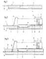
- FIG. 1 shows the carrier plate with copper / ceramic / copper layer sequence
- FIG. 2 shows the carrier plate with the multi-layer hybrid installed, and an assembled carrier plate with ceramic / copper / ceramic layer sequence.
- FIG. 1 shows the carrier plate 1, on which a multi-layer hybrid is mounted.
- This carrier plate 1 consists of a Ceramic plate 2, which is about 0.3 to 2 mm thick.
- This ceramic plate 2 is coated on both sides with a copper foil 3.
- the ceramic plate 2 can have recesses 4, which are then from the copper foils 3 are spanned.
- FIG. 2 shows the carrier plate 1 with mounted multi-layer hybrid 5.
- a multi-layer hybrid 5 usually consists of ceramic, where various components, such as resistors and capacitors are placed in different layers.
- the connections of the multi-layer hybrid 5 are not shown via wires 6 with External connections outside of the multi-layer hybrid or with corresponding Conductors of the structured copper foil 2 connected.
- the Multi-layer hybrid 5 are two power semiconductor devices in IC version attached in different ways. That's how a performance IC is 7 applied to the top of the multi-layer hybrid and by means of bonding wires 8 with conductor tracks on the upper side of the multi-layer hybrid 5 contacted.
- the Multi-layer hybrids 5 When assembling the multi-layer hybrid 5 on the Carrier plate 1 are now according to the invention on the back of the Multi-layer hybrids 5 mounted power IC's 10 over the cutouts 4 brought the ceramic plate 2 that they the copper foil 3rd press into the recess 4 so that a recess is created, which corresponds exactly to the chip thickness of the power IC 10. Alternatively can be pre-embossed with appropriate tools will.
- the power ICs 10 are connected via a thermal paste 11 the copper foil 3 coupled.
- the multi-layer hybrid 5 is with one thermally conductive adhesive 12 attached to the carrier plate 1. In order to are not additional constructions for dissipating heat from the Power IC 10 required.
- the heat generated at the power IC 10 can be passed on directly to the surrounding carrier plate 1 and from there to the housing base plate of a switching device or the like be led away.
- protruding copper foil 3 as a connecting comb 3a form, so that a simple contact to the External connections without additional bond wires is possible.
- FIG. 3 shows the multilayer hybrid 5 on a carrier plate 1a Ceramic-copper-ceramic layer sequence, i.e. is a copper foil 3 coated on both sides with ceramic 2, the ceramic thickness in each case is set according to the IC thickness.
- the IC 10 is here also coupled to the copper foil 3 via a thermal paste 11, during the multi-layer hybrid 5 with thermally conductive adhesive 12 is glued to the carrier plate.
- the contacting of the multi-layer hybrid takes place via the bond wires 6 and corresponding Contact recesses 13 on the copper foil 3. But it is the same also possible to connect the bonding wire 6 to an external contact e.g. one Lead connector.
- the adhesive for attaching the multi-layer hybrid can be applied to the carrier plate 1; la be applied flat, so that - according to figure 3 - an adhesive surface corresponding to the size of the multi-layer hybrid arises. But locally distributed according to FIG. 2 are also conceivable Glue dots.
Landscapes
- Engineering & Computer Science (AREA)
- Microelectronics & Electronic Packaging (AREA)
- Production Of Multi-Layered Print Wiring Board (AREA)
- Structure Of Printed Boards (AREA)
- Cooling Or The Like Of Semiconductors Or Solid State Devices (AREA)
Abstract
Description
Claims (7)
- Montageeinheit für Mehrlagenhybrid mit Halbleiter-Leistungsbauelementen in IC-Ausführungen, welcher auf einer Trägerplatte befestigt ist, dadurch gekennzeichnet, daß die Trägerplatte (1) eine beidseitig mit Kupferfolie (3) beschichtete Keramikplatte (2) ist und Aussparungen (4) aufweist, die mit Kupferfolie (3) überspannt sind, wobei die Kupferfolie (3) nach der Montage durch die auf der Rückseite des Mehrlagenhybrids (5) befestigten Leistungs-Halbleiterbauelemente (10) in die Aussparungen gedrückt ist, so daß die Kupferfolie (3) sich der Chipdicke des Leistungs-Halbleiterbauelementes (10) anpaßt.
- Montageeinheit für Mehrlagenhybride mit Halbleiter-Leistungsbauelementen in IC-Ausführungen, welcher auf einer Trägerplatte befestigt ist, dadurch gekennzeichnet, daß die Trägerplatte (la) eine beidseitig mit Keramik beschichtete Kupferfolie (3) ist und Aussparungen aufweist, in die die auf der Rückseite des Mehrlagenhybrids befestigten Halbleiter-Leistungsbauelemente (10) eingesetzt und über Bonddrähte (6) mit der Kupferfolie (3) kontaktiert sind.
- Montageeinheit nach Anspruch 1 und 2, dadurch gekennzeichnet, daß der Mehrlagenhybrid mit seinen auf der der Trägerplatte zugewandten Seite angeordneten Halbleiter-Leistungsbauelementen (10) auf die Trägerplatte (1) geklebt ist.
- Montageeinheit nach Anspruch 1 und 2, dadurch gekennzeichnet, daß der Mehrlagenhybrid (5) mit seinen auf der der Trägerplatte zugewandten Seite angeordneten Halbleiter-Leistungsbauelementen (10) mittels Wärmeleitpaste (11) an die Trägerplatte (1) angekoppelt ist.
- Montageeinheit nach Anspruch 1, dadurch gekennzeichnet, daß die Keramikplatte (2) ca. 0,3 bis 2 mm dick ist.
- Montageeinheit nach einem der vorhergehenden Ansprüche, dadurch gekennzeichnet, daß die Kupferfolie (3) eine Leiterbahnstrukturierung aufweist.
- Montageeinheit nach einem der vorhergehenden Ansprüche, dadurch gekennzeichnet, daß die Kupferfolie (3) als Kammanschluß (3a) nach außen geführt ist.
Applications Claiming Priority (3)
| Application Number | Priority Date | Filing Date | Title |
|---|---|---|---|
| DE4222474 | 1992-07-09 | ||
| DE4222474A DE4222474A1 (de) | 1992-07-09 | 1992-07-09 | Montageeinheit für Mehrlagenhybrid mit Leistungsbauelementen |
| PCT/DE1993/000548 WO1994001889A1 (de) | 1992-07-09 | 1993-06-24 | Montageeinheit für mehrlagenhybrid mit leistungsbauelementen |
Publications (2)
| Publication Number | Publication Date |
|---|---|
| EP0649565A1 EP0649565A1 (de) | 1995-04-26 |
| EP0649565B1 true EP0649565B1 (de) | 1998-09-30 |
Family
ID=6462783
Family Applications (1)
| Application Number | Title | Priority Date | Filing Date |
|---|---|---|---|
| EP93912615A Expired - Lifetime EP0649565B1 (de) | 1992-07-09 | 1993-06-24 | Montageeinheit für mehrlagenhybrid mit leistungsbauelementen |
Country Status (5)
| Country | Link |
|---|---|
| US (1) | US5576934A (de) |
| EP (1) | EP0649565B1 (de) |
| JP (1) | JP3285864B2 (de) |
| DE (2) | DE4222474A1 (de) |
| WO (1) | WO1994001889A1 (de) |
Cited By (1)
| Publication number | Priority date | Publication date | Assignee | Title |
|---|---|---|---|---|
| WO2006035017A1 (de) * | 2004-09-29 | 2006-04-06 | Robert Bosch Gmbh | Elektronisches gerät mit einem mehrschichtigen keramiksubstrat und einem entwärmungskörper |
Families Citing this family (32)
| Publication number | Priority date | Publication date | Assignee | Title |
|---|---|---|---|---|
| DE4444680A1 (de) * | 1994-12-15 | 1996-06-27 | Schulz Harder Juergen | Mehrfachsubstrat für elektrische Bauelemente, insbesondere für Leistungs-Bauelemente |
| DE19520676A1 (de) * | 1995-06-07 | 1996-12-12 | Deutsche Telekom Ag | Hybridschaltung und Verfahren zur Herstellung derselben |
| DE19629630A1 (de) * | 1996-07-23 | 1997-09-11 | Bosch Gmbh Robert | Steuergeräteanordnung mit einem elektrischen Anbaugerät |
| JPH1050926A (ja) * | 1996-07-31 | 1998-02-20 | Taiyo Yuden Co Ltd | ハイブリッドモジュール |
| US6323549B1 (en) * | 1996-08-29 | 2001-11-27 | L. Pierre deRochemont | Ceramic composite wiring structures for semiconductor devices and method of manufacture |
| WO1998030072A1 (en) * | 1996-12-30 | 1998-07-09 | Derochemont L Pierre Doing Bus | Ceramic composite wiring structures for semiconductor devices and method of manufacture |
| RU2161347C2 (ru) * | 1996-10-10 | 2000-12-27 | Самсунг Электроникс Ко., Лтд | Мощная гибридная интегральная схема |
| RU2185687C2 (ru) * | 1996-10-10 | 2002-07-20 | Самсунг Электроникс Ко., Лтд. | Мощная гибридная интегральная схема свч диапазона |
| RU2183367C2 (ru) * | 1996-10-10 | 2002-06-10 | Самсунг Электроникс Ко., Лтд. | Гибридная интегральная схема свч диапазона |
| RU2161346C2 (ru) * | 1996-10-10 | 2000-12-27 | Самсунг Электроникс Ко., Лтд. | Мощная гибридная интегральная схема свч-диапазона |
| US6204555B1 (en) * | 1996-10-10 | 2001-03-20 | Samsung Electronics Co., Ltd. | Microwave-frequency hybrid integrated circuit |
| SE510861C2 (sv) * | 1997-07-11 | 1999-06-28 | Ericsson Telefon Ab L M | Anordning och förfarande i elektroniksystem |
| DE19740330A1 (de) * | 1997-09-13 | 1999-03-25 | Bosch Gmbh Robert | Trägerplatte für Mikrohybridschaltungen |
| US6147869A (en) * | 1997-11-24 | 2000-11-14 | International Rectifier Corp. | Adaptable planar module |
| EP1018146B1 (de) * | 1998-05-28 | 2010-04-21 | DET International Holding Limited | Anordnung für elektrische Bauteile |
| US6466454B1 (en) | 1999-05-18 | 2002-10-15 | Ascom Energy Systems Ag | Component transformer |
| US5973923A (en) * | 1998-05-28 | 1999-10-26 | Jitaru; Ionel | Packaging power converters |
| US6255899B1 (en) | 1999-09-01 | 2001-07-03 | International Business Machines Corporation | Method and apparatus for increasing interchip communications rates |
| US6262481B1 (en) * | 2000-02-28 | 2001-07-17 | Harvatek Corporation | Folded heat sink for semiconductor device package |
| DE10035399A1 (de) * | 2000-07-19 | 2002-01-31 | Alcatel Sa | Subträger, elektronische Baugruppe und Verfahren zur Herstellung derselben |
| US6459586B1 (en) * | 2000-08-15 | 2002-10-01 | Galaxy Power, Inc. | Single board power supply with thermal conductors |
| US6518868B1 (en) | 2000-08-15 | 2003-02-11 | Galaxy Power, Inc. | Thermally conducting inductors |
| US6414847B1 (en) * | 2001-04-09 | 2002-07-02 | Agilent Technologies, Inc. | Integral dielectric heatspreader |
| JP2004361308A (ja) * | 2003-06-06 | 2004-12-24 | Fuji Electric Device Technology Co Ltd | 物理量検出装置および物理量検出手段格納ケース |
| JP4311243B2 (ja) * | 2004-03-15 | 2009-08-12 | 株式会社デンソー | 電子機器 |
| WO2008003549A1 (de) * | 2006-07-06 | 2008-01-10 | Continental Automotive Gmbh | Verfahren zum verkleben mindestens einer ersten platte und einer zweiten platte und verfahren zum herstellen einer leiterträgeranordnung |
| US7561430B2 (en) * | 2007-04-30 | 2009-07-14 | Watlow Electric Manufacturing Company | Heat management system for a power switching device |
| CN103035590A (zh) * | 2012-12-25 | 2013-04-10 | 浙江大学 | 一种igbt功率模块 |
| KR20160050950A (ko) * | 2014-10-31 | 2016-05-11 | 현대모비스 주식회사 | 인덕터 방열 장치를 구비하는 dc-dc 컨버터 |
| DE102016119485A1 (de) | 2016-10-12 | 2018-04-12 | Infineon Technologies Ag | Chipträger mit elektrisch leitfähiger Schicht, die sich über eine wärmeleitfähige dielektrische Sheet-Struktur hinaus erstreckt |
| DE102019121229B4 (de) * | 2019-08-06 | 2025-08-14 | Infineon Technologies Ag | Elektronische Vorrichtungen mit elektrisch isolierten Lastelektroden und zugehörige Herstellungsverfahren |
| DE102024205615A1 (de) * | 2024-06-18 | 2025-12-18 | Robert Bosch Gesellschaft mit beschränkter Haftung | Durchkontaktiertes Oberseitensubstrat eines Leistungsmoduls |
Family Cites Families (12)
| Publication number | Priority date | Publication date | Assignee | Title |
|---|---|---|---|---|
| DE1627762B2 (de) * | 1966-09-17 | 1972-11-23 | Nippon Electric Co. Ltd., Tokio | Verfahren zur Herstellung einer Halbleitervorrichtung |
| GB2111312A (en) * | 1981-11-04 | 1983-06-29 | Philips Electronic Associated | Substrates for electrical circuits |
| US4563383A (en) * | 1984-03-30 | 1986-01-07 | General Electric Company | Direct bond copper ceramic substrate for electronic applications |
| US4862323A (en) * | 1984-04-12 | 1989-08-29 | Olin Corporation | Chip carrier |
| US5012324A (en) * | 1987-07-03 | 1991-04-30 | Doduco Gmbh And Co. Dr. Eugen Durrwachter | Flat body, particularly for use as a heat sink for electronic power components |
| USH650H (en) * | 1988-04-14 | 1989-07-04 | The United States Of America As Represented By The United States Department Of Energy | Double sided circuit board and a method for its manufacture |
| US5055967A (en) * | 1988-10-26 | 1991-10-08 | Texas Instruments Incorporated | Substrate for an electrical circuit system and a circuit system using that substrate |
| JPH03211757A (ja) * | 1989-12-21 | 1991-09-17 | General Electric Co <Ge> | 気密封じの物体 |
| EP0434264B1 (de) * | 1989-12-22 | 1994-10-12 | Westinghouse Electric Corporation | Gehäuse für Leistungshalbleiterbauelemente |
| JPH079966B2 (ja) * | 1990-07-31 | 1995-02-01 | 三洋電機株式会社 | 混成集積回路の製造方法 |
| DE4031733A1 (de) * | 1990-10-06 | 1992-04-09 | Bosch Gmbh Robert | Mehrlagenhybride mit leistungsbauelementen |
| US5151769A (en) * | 1991-04-04 | 1992-09-29 | General Electric Company | Optically patterned RF shield for an integrated circuit chip for analog and/or digital operation at microwave frequencies |
-
1992
- 1992-07-09 DE DE4222474A patent/DE4222474A1/de not_active Withdrawn
-
1993
- 1993-06-24 DE DE59309029T patent/DE59309029D1/de not_active Expired - Fee Related
- 1993-06-24 EP EP93912615A patent/EP0649565B1/de not_active Expired - Lifetime
- 1993-06-24 US US08/367,181 patent/US5576934A/en not_active Expired - Fee Related
- 1993-06-24 JP JP50281294A patent/JP3285864B2/ja not_active Expired - Fee Related
- 1993-06-24 WO PCT/DE1993/000548 patent/WO1994001889A1/de not_active Ceased
Cited By (1)
| Publication number | Priority date | Publication date | Assignee | Title |
|---|---|---|---|---|
| WO2006035017A1 (de) * | 2004-09-29 | 2006-04-06 | Robert Bosch Gmbh | Elektronisches gerät mit einem mehrschichtigen keramiksubstrat und einem entwärmungskörper |
Also Published As
| Publication number | Publication date |
|---|---|
| JPH07508858A (ja) | 1995-09-28 |
| WO1994001889A1 (de) | 1994-01-20 |
| US5576934A (en) | 1996-11-19 |
| DE4222474A1 (de) | 1994-01-13 |
| EP0649565A1 (de) | 1995-04-26 |
| DE59309029D1 (de) | 1998-11-05 |
| JP3285864B2 (ja) | 2002-05-27 |
Similar Documents
| Publication | Publication Date | Title |
|---|---|---|
| DE4222474A1 (de) | Montageeinheit für Mehrlagenhybrid mit Leistungsbauelementen | |
| EP1255299B1 (de) | Leistungshalbleitermodul in Druckkontaktierung | |
| DE19700963C2 (de) | Verfahren zur Herstellung eines Leistungsmoduls mit einer aktive Halbleiterbauelemente und passive Halbleiterbauelemente aufweisenden Schaltungsanordnung | |
| EP0855090B1 (de) | Multichipmodul | |
| EP1351302B1 (de) | Leistungshalbleitermodul | |
| EP0805494B1 (de) | Halbleiterleistungsmodul hoher Packungsdichte in Mehrschichtbauweise | |
| DE10306643B4 (de) | Anordnung in Druckkontaktierung mit einem Leistungshalbleitermodul | |
| EP0558712B1 (de) | Elektrisches gerät, insbesondere schalt- und steuergerät für kraftfahrzeuge | |
| WO1998015005A9 (de) | Mikroelektronisches bauteil in sandwich-bauweise | |
| EP0935818B1 (de) | Elektronisches steuergerät | |
| EP0368143A2 (de) | Elektronisches Steuergerät | |
| DE19722357C1 (de) | Steuergerät | |
| DE19859739A1 (de) | Kühlvorrichtung, insbesondere zur Verwendung in einem elektronischen Steuergerät | |
| DE4031733A1 (de) | Mehrlagenhybride mit leistungsbauelementen | |
| DE3444699C2 (de) | ||
| DE102004018471B4 (de) | Leistungshalbleiterschaltung und Verfahren zum Herstellen einer Leistungshalbleiterschaltung | |
| DE10129006B4 (de) | Elektronische Baugruppe | |
| DE19857959A1 (de) | Elektronisches Steuergerät | |
| DD248907A1 (de) | Bauelementetraegerplatte zur montage von halbleiterchips im scheibenverband | |
| WO2007045112A1 (de) | Leistungsgehäuse für halbleiterchips und deren anordnung zur wärmeabfuhr | |
| DE19735074A1 (de) | Leistungsmodul | |
| DE4103486A1 (de) | Anordnung zur kuehlung waermeerzeugender bauelemente | |
| WO2003071601A2 (de) | Schaltungsmodul und verfahren zu seiner herstellung | |
| DE102010000035B4 (de) | Verfahren zur Herstellung einer Elektronikbaugruppe und eine nach dem Verfahren hergestellte Elektronikbaugruppe | |
| WO2006035017A1 (de) | Elektronisches gerät mit einem mehrschichtigen keramiksubstrat und einem entwärmungskörper |
Legal Events
| Date | Code | Title | Description |
|---|---|---|---|
| PUAI | Public reference made under article 153(3) epc to a published international application that has entered the european phase |
Free format text: ORIGINAL CODE: 0009012 |
|
| 17P | Request for examination filed |
Effective date: 19950209 |
|
| AK | Designated contracting states |
Kind code of ref document: A1 Designated state(s): DE FR GB IT |
|
| 17Q | First examination report despatched |
Effective date: 19960329 |
|
| GRAG | Despatch of communication of intention to grant |
Free format text: ORIGINAL CODE: EPIDOS AGRA |
|
| GRAG | Despatch of communication of intention to grant |
Free format text: ORIGINAL CODE: EPIDOS AGRA |
|
| GRAH | Despatch of communication of intention to grant a patent |
Free format text: ORIGINAL CODE: EPIDOS IGRA |
|
| GRAH | Despatch of communication of intention to grant a patent |
Free format text: ORIGINAL CODE: EPIDOS IGRA |
|
| GRAA | (expected) grant |
Free format text: ORIGINAL CODE: 0009210 |
|
| AK | Designated contracting states |
Kind code of ref document: B1 Designated state(s): DE FR GB IT |
|
| REF | Corresponds to: |
Ref document number: 59309029 Country of ref document: DE Date of ref document: 19981105 |
|
| ET | Fr: translation filed | ||
| GBT | Gb: translation of ep patent filed (gb section 77(6)(a)/1977) |
Effective date: 19981201 |
|
| PLBE | No opposition filed within time limit |
Free format text: ORIGINAL CODE: 0009261 |
|
| STAA | Information on the status of an ep patent application or granted ep patent |
Free format text: STATUS: NO OPPOSITION FILED WITHIN TIME LIMIT |
|
| 26N | No opposition filed | ||
| REG | Reference to a national code |
Ref country code: GB Ref legal event code: IF02 |
|
| PGFP | Annual fee paid to national office [announced via postgrant information from national office to epo] |
Ref country code: GB Payment date: 20030528 Year of fee payment: 11 |
|
| PGFP | Annual fee paid to national office [announced via postgrant information from national office to epo] |
Ref country code: FR Payment date: 20030619 Year of fee payment: 11 |
|
| PG25 | Lapsed in a contracting state [announced via postgrant information from national office to epo] |
Ref country code: GB Free format text: LAPSE BECAUSE OF NON-PAYMENT OF DUE FEES Effective date: 20040624 |
|
| GBPC | Gb: european patent ceased through non-payment of renewal fee |
Effective date: 20040624 |
|
| PG25 | Lapsed in a contracting state [announced via postgrant information from national office to epo] |
Ref country code: FR Free format text: LAPSE BECAUSE OF NON-PAYMENT OF DUE FEES Effective date: 20050228 |
|
| REG | Reference to a national code |
Ref country code: FR Ref legal event code: ST |
|
| PG25 | Lapsed in a contracting state [announced via postgrant information from national office to epo] |
Ref country code: IT Free format text: LAPSE BECAUSE OF NON-PAYMENT OF DUE FEES;WARNING: LAPSES OF ITALIAN PATENTS WITH EFFECTIVE DATE BEFORE 2007 MAY HAVE OCCURRED AT ANY TIME BEFORE 2007. THE CORRECT EFFECTIVE DATE MAY BE DIFFERENT FROM THE ONE RECORDED. Effective date: 20050624 |
|
| PGFP | Annual fee paid to national office [announced via postgrant information from national office to epo] |
Ref country code: DE Payment date: 20070828 Year of fee payment: 15 |
|
| PG25 | Lapsed in a contracting state [announced via postgrant information from national office to epo] |
Ref country code: DE Free format text: LAPSE BECAUSE OF NON-PAYMENT OF DUE FEES Effective date: 20090101 |