EP1353237A2 - Appareil et méthode de détermination du type de matériel d'enregistrement et appareil de formation d'images - Google Patents
Appareil et méthode de détermination du type de matériel d'enregistrement et appareil de formation d'images Download PDFInfo
- Publication number
- EP1353237A2 EP1353237A2 EP03008361A EP03008361A EP1353237A2 EP 1353237 A2 EP1353237 A2 EP 1353237A2 EP 03008361 A EP03008361 A EP 03008361A EP 03008361 A EP03008361 A EP 03008361A EP 1353237 A2 EP1353237 A2 EP 1353237A2
- Authority
- EP
- European Patent Office
- Prior art keywords
- recording material
- recording
- calculation
- irregularities
- read
- Prior art date
- Legal status (The legal status is an assumption and is not a legal conclusion. Google has not performed a legal analysis and makes no representation as to the accuracy of the status listed.)
- Granted
Links
- 239000000463 material Substances 0.000 title claims abstract description 182
- 238000000034 method Methods 0.000 title claims abstract description 18
- 238000004364 calculation method Methods 0.000 claims abstract description 112
- 238000010586 diagram Methods 0.000 description 13
- 239000000835 fiber Substances 0.000 description 7
- 238000003384 imaging method Methods 0.000 description 6
- 238000006243 chemical reaction Methods 0.000 description 4
- 230000003287 optical effect Effects 0.000 description 4
- 238000005070 sampling Methods 0.000 description 2
- 230000001133 acceleration Effects 0.000 description 1
- 230000015556 catabolic process Effects 0.000 description 1
- 239000003086 colorant Substances 0.000 description 1
- 238000011109 contamination Methods 0.000 description 1
- 238000006731 degradation reaction Methods 0.000 description 1
- 238000001514 detection method Methods 0.000 description 1
- 235000019800 disodium phosphate Nutrition 0.000 description 1
- 239000000428 dust Substances 0.000 description 1
- 239000000976 ink Substances 0.000 description 1
- 239000011159 matrix material Substances 0.000 description 1
- 238000012986 modification Methods 0.000 description 1
- 230000004048 modification Effects 0.000 description 1
- 239000003973 paint Substances 0.000 description 1
- 230000001360 synchronised effect Effects 0.000 description 1
Images




Classifications
-
- G—PHYSICS
- G03—PHOTOGRAPHY; CINEMATOGRAPHY; ANALOGOUS TECHNIQUES USING WAVES OTHER THAN OPTICAL WAVES; ELECTROGRAPHY; HOLOGRAPHY
- G03G—ELECTROGRAPHY; ELECTROPHOTOGRAPHY; MAGNETOGRAPHY
- G03G15/00—Apparatus for electrographic processes using a charge pattern
-
- G—PHYSICS
- G03—PHOTOGRAPHY; CINEMATOGRAPHY; ANALOGOUS TECHNIQUES USING WAVES OTHER THAN OPTICAL WAVES; ELECTROGRAPHY; HOLOGRAPHY
- G03G—ELECTROGRAPHY; ELECTROPHOTOGRAPHY; MAGNETOGRAPHY
- G03G15/00—Apparatus for electrographic processes using a charge pattern
- G03G15/50—Machine control of apparatus for electrographic processes using a charge pattern, e.g. regulating differents parts of the machine, multimode copiers, microprocessor control
- G03G15/5029—Machine control of apparatus for electrographic processes using a charge pattern, e.g. regulating differents parts of the machine, multimode copiers, microprocessor control by measuring the copy material characteristics, e.g. weight, thickness
-
- G—PHYSICS
- G03—PHOTOGRAPHY; CINEMATOGRAPHY; ANALOGOUS TECHNIQUES USING WAVES OTHER THAN OPTICAL WAVES; ELECTROGRAPHY; HOLOGRAPHY
- G03G—ELECTROGRAPHY; ELECTROPHOTOGRAPHY; MAGNETOGRAPHY
- G03G2215/00—Apparatus for electrophotographic processes
- G03G2215/00362—Apparatus for electrophotographic processes relating to the copy medium handling
- G03G2215/00535—Stable handling of copy medium
- G03G2215/00611—Detector details, e.g. optical detector
- G03G2215/00616—Optical detector
-
- G—PHYSICS
- G03—PHOTOGRAPHY; CINEMATOGRAPHY; ANALOGOUS TECHNIQUES USING WAVES OTHER THAN OPTICAL WAVES; ELECTROGRAPHY; HOLOGRAPHY
- G03G—ELECTROGRAPHY; ELECTROPHOTOGRAPHY; MAGNETOGRAPHY
- G03G2215/00—Apparatus for electrophotographic processes
- G03G2215/00362—Apparatus for electrophotographic processes relating to the copy medium handling
- G03G2215/00535—Stable handling of copy medium
- G03G2215/00717—Detection of physical properties
- G03G2215/00751—Detection of physical properties of sheet type, e.g. OHP
Definitions
- the present invention relates to a recording-material type determination apparatus, recording-material type determination method, and image forming apparatus such as a copier or laser printer which controls imaging conditions using the recording-material type determination apparatus.
- such an image forming apparatus controls to set fixing conditions (e.g. fixing temperature and conveying speed of the recording paper passing through the fixing apparatus) according to user settings after the user sets a size and type (also called a paper type) of the recording paper, which is recording material, on a control panel or the like installed, for example, on the image forming apparatus main body.
- fixing conditions e.g. fixing temperature and conveying speed of the recording paper passing through the fixing apparatus
- a size and type also called a paper type
- an image forming apparatus incorporates a sensor for determining recording material and controls developing conditions, fixing conditions or transfer conditions variably according to the type of recording material.
- Japanese Patent Application Laid-Open No. 11-27103 proposes a technique for picking up a surface picture of recording material using a CCD sensor, converting it into fractal dimension information, and thereby detecting the surface flatness of the recording material.
- the image forming apparatus has the following problems.
- the present invention has been made in view of the above circumstances. Its object is to provide a recording-material type determination apparatus and recording-material type determination method which can determine the. type of recording material (i.e., determine the flatness of recording material) using simple calculations as well as to provide an image forming apparatus capable of obtaining stable image quality independent of the type of recording material using the apparatus and method.
- Another object of the present invention is to provide a recording material type determination apparatus comprising: a light emit unit, adapted to illuminate a surface of recording material; a read unit, adapted to read an illuminated region on the surface of the recording material as a video image; a first calculation unit adapted to calculate information about depth of irregularities in the surface of the recording material based on video information read by the read unit; a second calculation unit adapted to calculate information about spacing of irregularities on the surface of the recording material based on the video information read by the read unit; and a determination unit adapted to determine a type of recording material based on calculation results produced by the first calculation unit and the second calculation unit.
- Yet another object of the present invention is to provide a recording-material type determination apparatus comprising: an input unit adapted to input a video image of a surface of recording material; a first calculation unit adapted to calculate information about depth of irregularities in a surface of the recording material based on video information inputted in the input unit; a second calculation unit adapted to calculate information about spacing of irregularities on the surface of the recording material based on the video information inputted in the input unit; and a determination unit adapted to determine a type of recording material based on calculation results produced by the first calculation unit and the second calculation unit.
- Yet another object of the present invention is to provide a recording-material type determination method comprising: a read step of reading a surface of recording material as a video image; a first calculation step of calculating information about depth of irregularities in the surface of the recording material based on results of the read step; a second calculation step of calculating information about spacing of irregularities on the surface of the recording material based on the results of the read step; and a determination step of determining a type of recording material based on calculation results produced in the first calculation step and the second calculation step.
- Yet another object of the present invention is to provide an image forming apparatus comprising: a conveyor adapted to convey recording material; an image forming unit which forms an image on the recording material conveyed by the conveyor; a light emit unit, adapted to illuminate a surface of recording material; a read unit, adapted to read an illuminated region on the surface of the recording material as a video image; a first calculation unit adapted to calculate information about depth of irregularities in the surface of the recording material based on video information read by the read unit; a second calculation unit adapted to calculate information about spacing of irregularities on the surface of the recording material based on the video information read by the read unit; a determination unit adapted to determine a type of recording material based on calculation results produced by the first calculation unit and the second calculation unit; and a controller which controls image forming conditions of the image forming unit based on the type of recording material determined by the determination unit.
- FIG. 1 is a block diagram showing configuration of a "recording-material type determination apparatus" according to a first example.
- control circuit block which performs first calculation and second calculation and determines the type of recording material.
- reference numeral 701 denotes a CPU which serves as a determination part
- 702 denotes a control circuit
- 703 denotes a CMOS area sensor
- 704 denotes an interface control circuit
- 705 denotes a calculation circuit
- 706 denotes a register A which stores results of calculation on the amount of irregularities in the surface of recording material carried out by first calculation means (means of calculating the depth of irregularities in the surface of recording material)
- 707 denotes a register B which stores results of calculation on the edge amount of irregularities in the surface of recording material carried out by second calculation means (means of calculating the spacing of irregularities on the surface of recording material)
- 708 denotes a control register.
- Reference numeral 709 denotes a ROM (memory part) which prestores programs to be executed by the CPU 701 as well as reference information about various recording materials (described later).
- the CPU 701 instructs the control register 708 to operate the CMOS area sensor 703
- the CMOS area sensor 703 starts picking up (taking) a picture of the recording material.
- the CMOS area sensor 703 starts to accumulate charge.
- the CMOS area sensor 703 is selected at SL_select sent by the interface control circuit 704, SYSCLK is generated at a predetermined time, and digital image data picked up is transmitted by the CMOS area sensor 703 using an SL_out signal.
- the imaging data received via the interface control circuit 704 is calculated by the calculation circuit 705 in the control circuit 702 using a first calculation method described later and the results are stored in the register A 706 as the amount of irregularities in the surface of the recording material.
- the imaging data received via the interface control circuit 704 and calculated by the calculation circuit 705 in the control circuit 702 using a second calculation method described later is stored in the register B 707 as the edge amount of irregularities in the surface of the recording material.
- the CPU 701 judges the type of recording material based on the values of the two registers A and B.
- CMOS area sensor 703 serving as an image sensor will be described with reference to FIG. 2.
- reference numeral 30 denotes a sensor unit
- 31 denotes a recording-paper convey guide
- 32 denotes recording material
- 33 denotes an LED serving as lighting means
- 34 denotes a CMOS area sensor
- 35 and 36 denote lenses.
- Light from the LED light source illuminates the surface of the convey guide 31 or the surface of the recording material 32 via the lens 35.
- Reflected light from the recording material 32 is collected via the lens 36 and is focused onto the CMOS area sensor 34 to allow a surface image to be read from the recording-paper convey guide 31 or recording material 32.
- the LED 33 is placed in such a way that its light will fall on the surface of the recording material at an oblique angle as shown in the figure.
- Reference numerals 43 to 45 in FIGS. 3A to 3F denote images resulting from digital processing of surface images read by the 8 ⁇ 8 pixels CMOS area sensor 34 from the recording material.
- the digital processing consists of converting analog output of a sensor part of the CMOS area sensor 34 into 8-bit pixel data by means of A/D conversion.
- Reference numeral 40 denotes recording material A, so-called rough paper, whose surface fibers are relatively rough.
- Reference numeral 41 denotes recording material B, so-called plain paper, which is in common use.
- Reference numeral 42 denotes an enlarged view of a surface of recording material C, so-called gloss paper, whose fibers have been compressed adequately.
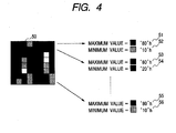
- reference numeral 50 denotes an image obtained by digitally processing a video image of the surface of the recording material.
- Analog data outputted from the sensor part of the CMOS area sensor is converted into 8-bit pixel data by means of A/D conversion.
- the 8-bit data is determined in proportion to the brightness of the image.
- Reference numeral 51 denotes the darkest part in the first line of the 8 ⁇ 8 pixels. Its value is '80'h in the example of FIG. 4.
- reference numeral 53 denotes the darkest part in the second line. Its value is '80'h.
- Reference numeral 55 denotes the darkest part in the eighth line. Its value is '80'h.
- the difference between the maximum value and minimum value is added for each line and the resulting value for all the lines is defined as the result of the calculation carried out by the first calculation means on the amount of irregularities in the surface of the recording material.
- calculation circuit 705 as second calculation means calculates the spacing of irregularities on the surface of the recording material (edge amount).
- Reference numeral 50 denotes an image obtained by digitally processing the surface of the recording material.
- Reference numeral 60 denotes an image obtained by binarizing 8 ⁇ 8 pixels picked up at the next sampling time using, as a threshold, an average calculated from the image 50 picked up beforehand at the previous sampling time.
- Edge numbers obtained as a result of binarization are as follows.
- Reference numeral 61 denotes the edge number in the first line, which is '05'h in this example.
- Reference numeral 62 denotes the edge number in the second line, which is '03'h in this example.
- reference numeral 63 denotes the edge number in the eighth line, which is '03'h in this example.
- the edge number is counted for each line and the resulting value for all the lines is defined as the result of the calculation carried out by the second calculation means on the edge amount on the surface of the recording material.
- the edge amount of irregularities is inversely proportional to the spacing of irregularities and in this example, information about the spacing of irregularities is obtained by calculating the edge amount.
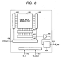
- the CMOS area sensor 703 will be described with reference to FIG. 6.
- FIG. 6 is a block diagram showing configuration of the CMOS area sensor 703.
- reference numeral 601 denotes a CMOS area sensor part where, for example, sensors for 8 ⁇ 8 pixels are arranged in a matrix.
- Reference numerals 602 and 603 denote vertical shift registers, 604 denotes an output buffer, 605 denotes a horizontal shift register, 606 denotes a system clock, 607 denotes a timing generator.
- the data placed in the output buffer 604 is transferred to an A/D converter 608 by the horizontal shift register 605. After digital conversion by the A/D converter 608, resulting pixel data is controlled with predetermined timing by an output interface circuit 609 and outputted as the SL_out signal 610 during a period when the SL_select signal 613 is active.
- a control circuit 611 can control A/D conversion gain variably using an SL_in signal 612. For example, if contrast of an image is not available, the CPU 701 can pick up the image always using the best contrast by changing gain.
- FIG. 7 is a diagram showing distribution of recording materials together with video images of their actual surfaces, wherein the horizontal axis represents the value of the register A, i.e., the result of calculation carried out by the first calculation means on the amount of irregularities in the surface of the recording material while the vertical axis represents the value of the register B, i.e., the result of calculation carried out by the second calculation means on the edge amount of irregularities in the surface of the recording material.
- Reference numeral 801 denotes gloss paper
- 802 denotes plain paper
- 803 denotes rough paper
- 804 denotes OHT.
- the value of the register A is larger than that of the gloss paper 801 and the value of the register B is smaller than that of the gloss paper 801 as can be seen from the video image of its surface.
- the rough paper 803 has a larger register A value than the plain paper 802 and a smaller register B value than the plain paper 802.
- Prescribed reference information about the amount of irregularities and the edge amount of irregularities of each recording material is prestored in the ROM (memory unit) 709 shown in FIG. 1.
- the CPU 701 reads the value stored in the resister A and value stored in the resister B in sequence by sending a read signal to the control register and then determines the type of recording material by comparing these values with the reference information stored in the ROM (memory unit) 709.
- the CPU 701 can detect surface characteristics, etc. of various recording materials by comparing the value of the register A, i.e., the result of calculation carried out by the first calculation means on the amount of irregularities in the surface of the recording material and the value of the register B, i.e., the result of calculation carried out by the second calculation means on the edge amount of irregularities on the surface of the recording material with the information stored in the ROM (memory unit) 709.
- the CPU 701 can determine recording material by distinguishing among gloss paper, plain paper, rough paper and OHT.
- the use of the edge amount of irregularities makes it possible to distinguish between the gloss paper 801 and OHT 804.
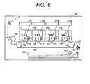
- FIG. 8 is a sectional view showing configuration of an "image forming apparatus" according to a second example.
- the recording-material type determination apparatus used in this example is the same as the first example, and thus its description will be quoted.
- reference numeral 101 denotes an image forming apparatus
- 102 denotes a paper cassette
- 103 denotes a paper feeding roller
- 104 denotes a transferring-belt driving roller
- 105 denotes a transferring belt
- 106 to 109 denote yellow, magenta, cyan and black photosensitive drums
- 110 to 113 denote transferring rollers
- 114 to 117 denote yellow, magenta, cyan and black cartridges
- 118 to 121 denote yellow, magenta, cyan and black optical units
- 122 denotes a fixing unit.
- the image forming apparatus uses an electrophotographic process to transfer yellow, magenta, cyan and black images onto recording paper by superimposing them and thermally fixes the toner images by a fixing roller under temperature control.
- the optical units for individual colors scan the respective photosensitive drums by exposing their surface to a laser beam to form latent images. These scanning operations for forming images are synchronized so that images will be transferred from preset positions on conveyed recording paper.
- the image forming apparatus comprises a paper feeding motor which feeds and conveys recording paper which is a recording material, transferring-belt driving motor which drives the transferring-belt driving roller, photosensitive-drum driving motor which drives the photosensitive drums for color inks and transferring roller, and fixing-roller driving motor which drives the fixing roller.
- Reference numeral 123 denotes an image sensor which illuminates the surface of recording paper being fed and conveyed, collects and focuses the light reflected from the surface, and thereby detects an image of a specific area on the recording paper.
- a control CPU (not shown) mounted on the image forming apparatus fuses and fixes the toner images on the recording paper by giving a desired quantity of heat to the recording paper using the fixing unit (part) 122.
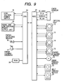
- FIG. 9 shows composition of units (parts) controlled by the control CPU.
- reference numeral 10 denotes a CPU; 11 denotes a CMOS sensor; 12 to 15 denote optical units which are equipped with a polygon mirror, motor and laser and paint desired latent images by scanning the surfaces of photosensitive drums with a laser; 16 denotes a paper feeding motor which feeds recording paper; 17 denotes a paper feeding solenoid used to start a paper feeding roller for feeding recording material; 18 denotes a paper detecting sensor which detects whether or not recording material is placed in position; 19 denotes a high voltage power supply which controls primary electrification, developing, primary transfer and a secondary transfer bias needed for an electrophotographic process; 20 denotes a drum driving motor which drives the photosensitive drums and transferring roller; 21 denotes a belt driving motor which drives the transferring belt and fixing unit roller; and 22 denotes a fixing unit and low voltage power supply unit which monitors temperature and keeps fixing temperature constant using a thermister (not shown)
- Reference numeral 23 denotes an ASIC which controls the speed of motors in the CMOS sensor 11 and optical units 12 to 15 as well as the speed of the paper feeding motor under instructions from the control CPU 10.
- tack signals from a motor are detected and acceleration signals or deceleration signals are output to the motors such that the interval between the tack signals has a predetermined duration.
- the control CPU 10 Upon receiving a print command from a host computer (not shown), the control CPU 10 makes the paper detecting sensor 18 judge whether or not recording material is present. If paper is present, the control CPU 10 drives the paper feeding motor 16, drum driving motor 20, belt driving motor 21 and paper feeding solenoid 17 to convey the recording material into position.
- the control CPU 10 instructs the ASIC 23 to make the CMOS sensor 11 pick up an image (taking a picture of a surface). Consequently, the CMOS sensor 11 picks up a surface image of the recording material.
- the ASIC 23 sets SL_select (see FIG. 1) active, outputs a predetermined SYSCLK pulse at a predetermined time, and captures imaging data outputted from the CMOS sensor 11 using SL_out.
- the gain of the CMOS sensor 11 is set as follows.
- the control CPU 10 sets a predetermined value in a register in the ASIC 23, the ASIC 23 sets SL_select active, outputs a predetermined SYSCLK pulse at a predetermined time, and sets the gain of the CMOS sensor 11 using SL_in.
- the ASIC 23 comprises circuits which serve as the first calculation means and the second calculation means described in the first example and calculation results produced by them are stored in registers in the ASIC 23.
- the CPU 10 reads the registers in the ASIC 23, determines the type of the recording material which has been fed, and variably controls developing-bias conditions of the high voltage power supply 19 according to the determined type.
- the CPU 10 sets the developing bias to a lower value than in the case of plain paper to prevent scattering of toner by reducing the amount of toner sticking to the surface of the recording material. This is done to solve the problem of degradation in image quality caused by toner scattering from paper fibers especially in the case of rough paper whose surface tend to collect a large amount of toner.
- the CPU 10 determines the type of the recording material which has been fed, and variably controls transfer conditions of transferring means according to the determined type.
- the CPU 10 determines the type of the recording material which has been fed, and variably controls temperature conditions of the fixing unit 22 according to the determined type.
- the CPU 10 determines the type of the recording material which has been fed, and variably controls the conveying speed of the recording material according to the determined type.
- the variable control of the conveying speed is achieved as the CPU 10 sets the value of a speed control register in the ASIC 23.
- this is effective in increasing the fixability of the toner which sticks to the recording material, improving gloss, and thereby improving image quality.
- the ASIC-based hardware circuit performs first calculation and second calculation based on the surface image of the recording material picked up by the CMOS area sensor, and the CPU variably controls the developing conditions and transfer conditions of the high voltage power supply, controlled-temperature conditions of the fixing unit, or conveying speed of the recording material based on the calculation results.
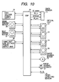
- FIG. 10 is diagram showing composition of units controlled by a control CPU in an "image forming apparatus" according to a third example.
- the recording-material type determination apparatus used in this example is the same as the first example, and thus its description will be quoted.
- reference numeral 24 denotes a digital signal processor.
- Reference numerals 11 to 22 denote the same components as those described in the second example, and thus description thereof will be omitted.
- the digital signal processor directly controls the image forming apparatus including motors as well as imaging information from the CMOS area sensor.
- the image captured by the CMOS area sensor 11 is processed by the DSP 24 using the first calculation means and the second calculation means. Consequently, the DSP 24 variably controls control conditions of the high voltage power supply 19, fixing unit 22, drum driving motor 20 and belt driving motor 21.
- DSP-based software control makes it possible to adjust calculation methods of the first calculation means and second calculation means flexibly.
- any contamination of the CMOS area sensor 11 or its lens with dust or other foreign matter may degrade the accuracy with which the surface characteristics of recording material are detected based on results of calculations carried out by the first calculation means and second calculation means.
- the above problem can be solved by picking up an image of the recording material as a reference image before the recording material passes through the CMOS area sensor 11 and subtracting the reference image from a surface image of the recording material.
- image forming apparatus can greatly improve the accuracy with which the type and surface characteristics of recording material are detected based on the calculations carried out by the first calculation means and second calculation means.
- the present invention provides a recording-material type determination apparatus and recording-material type determination method which can determine the type of recording material using simple calculations as well as provides an image forming apparatus capable of obtaining stable image quality independent of the type of recording material using the apparatus and method. Also, since the present invention determines the type of recording material from two standpoints-- namely, depth of irregularities in the surface of the recording material and spacing of irregularities on the surface of the recording material, it can determine the type of recording material more accurately.
- a first calculation unit calculates the depth of irregularities in the surface of recording material and stores the results of calculation in a register A while a second calculation unit calculates the spacing of irregularities on the surface of the recording material and stores the results of calculation in a register B. Based on the values in the registers A and B, the type of recording material such as gloss paper, plain paper, rough paper or OHT is determined.
Landscapes
- Physics & Mathematics (AREA)
- General Physics & Mathematics (AREA)
- Engineering & Computer Science (AREA)
- Microelectronics & Electronic Packaging (AREA)
- Control Or Security For Electrophotography (AREA)
- Fixing For Electrophotography (AREA)
- Developing For Electrophotography (AREA)
- Electrostatic Charge, Transfer And Separation In Electrography (AREA)
- Length Measuring Devices By Optical Means (AREA)
Priority Applications (1)
| Application Number | Priority Date | Filing Date | Title |
|---|---|---|---|
| EP11156229.4A EP2339406B1 (fr) | 2002-04-12 | 2003-04-10 | Appareil et méthode de détermination du type de matériel d'enregistrement et appareil de formation d'images |
Applications Claiming Priority (2)
| Application Number | Priority Date | Filing Date | Title |
|---|---|---|---|
| JP2002109922A JP4227351B2 (ja) | 2002-04-12 | 2002-04-12 | 記録材の種別判別装置および画像形成装置 |
| JP2002109922 | 2002-04-12 |
Related Child Applications (2)
| Application Number | Title | Priority Date | Filing Date |
|---|---|---|---|
| EP11156229.4A Division-Into EP2339406B1 (fr) | 2002-04-12 | 2003-04-10 | Appareil et méthode de détermination du type de matériel d'enregistrement et appareil de formation d'images |
| EP11156229.4A Division EP2339406B1 (fr) | 2002-04-12 | 2003-04-10 | Appareil et méthode de détermination du type de matériel d'enregistrement et appareil de formation d'images |
Publications (3)
| Publication Number | Publication Date |
|---|---|
| EP1353237A2 true EP1353237A2 (fr) | 2003-10-15 |
| EP1353237A3 EP1353237A3 (fr) | 2009-03-18 |
| EP1353237B1 EP1353237B1 (fr) | 2014-03-12 |
Family
ID=28449973
Family Applications (2)
| Application Number | Title | Priority Date | Filing Date |
|---|---|---|---|
| EP11156229.4A Expired - Lifetime EP2339406B1 (fr) | 2002-04-12 | 2003-04-10 | Appareil et méthode de détermination du type de matériel d'enregistrement et appareil de formation d'images |
| EP03008361.2A Expired - Lifetime EP1353237B1 (fr) | 2002-04-12 | 2003-04-10 | Appareil et méthode de détermination du type de matériel d'enregistrement et appareil de formation d'images |
Family Applications Before (1)
| Application Number | Title | Priority Date | Filing Date |
|---|---|---|---|
| EP11156229.4A Expired - Lifetime EP2339406B1 (fr) | 2002-04-12 | 2003-04-10 | Appareil et méthode de détermination du type de matériel d'enregistrement et appareil de formation d'images |
Country Status (5)
| Country | Link |
|---|---|
| US (3) | US6801727B2 (fr) |
| EP (2) | EP2339406B1 (fr) |
| JP (1) | JP4227351B2 (fr) |
| KR (1) | KR100514030B1 (fr) |
| CN (1) | CN1179193C (fr) |
Cited By (1)
| Publication number | Priority date | Publication date | Assignee | Title |
|---|---|---|---|---|
| EP2339406A1 (fr) | 2002-04-12 | 2011-06-29 | Canon Kabushiki Kaisha | Appareil et méthode de détermination du type de matériel d'enregistrement et appareil de formation d'images |
Families Citing this family (34)
| Publication number | Priority date | Publication date | Assignee | Title |
|---|---|---|---|---|
| US7339702B2 (en) * | 2002-04-25 | 2008-03-04 | Canon Kabushiki Kaisha | Picture reading device for discriminating the type of recording medium and apparatus thereof |
| US7110686B2 (en) * | 2003-07-31 | 2006-09-19 | Canon Kabushiki Kaisha | Image forming apparatus capable of changing usage ratio among multiple toners |
| JP4993653B2 (ja) * | 2003-10-03 | 2012-08-08 | キヤノン株式会社 | 記録材判別装置および画像形成装置並びにその方法 |
| JP4447887B2 (ja) * | 2003-10-27 | 2010-04-07 | キヤノン株式会社 | カラー画像形成装置及び色安定化制御方法 |
| JP4756227B2 (ja) | 2004-03-30 | 2011-08-24 | キヤノン株式会社 | 画像形成装置 |
| US7885597B2 (en) * | 2004-04-20 | 2011-02-08 | Hewlett-Packard Development Company, L.P. | Scanning a media stack |
| FR2879963B1 (fr) * | 2004-12-24 | 2008-09-12 | Mgi France Sa | Imprimante laser numerique et procede d'impression de documents |
| JP4738872B2 (ja) * | 2005-04-12 | 2011-08-03 | キヤノン株式会社 | 像加熱装置 |
| US7292796B2 (en) * | 2005-06-29 | 2007-11-06 | Xerox Corporation | Method and system for roller pair adjustment |
| US7551306B2 (en) * | 2005-07-29 | 2009-06-23 | Canon Kabushiki Kaisha | Image forming apparatus and method for controlling the image forming apparatus |
| JP4845656B2 (ja) * | 2006-09-14 | 2011-12-28 | キヤノン株式会社 | 画像形成装置 |
| US7945177B2 (en) | 2006-09-29 | 2011-05-17 | Canon Kabushiki Kaisha | Image forming apparatus with first and second settable resolution grades |
| US7750330B2 (en) | 2007-01-11 | 2010-07-06 | Canon Kabushiki Kaisha | Device and method for identifying recording medium and image forming apparatus |
| US7742712B2 (en) | 2007-01-29 | 2010-06-22 | Kabushiki Kaisha Toshiba | Transfer bias voltage controlling apparatus |
| US7865094B2 (en) * | 2007-02-23 | 2011-01-04 | Kabushiki Kaisha Toshiba | Image forming apparatus |
| JP5084316B2 (ja) * | 2007-03-22 | 2012-11-28 | キヤノン株式会社 | 画像形成装置 |
| US7877055B2 (en) * | 2007-04-11 | 2011-01-25 | Kabushiki Kaisha Toshiba | Paper type determination device |
| US7715740B2 (en) * | 2007-04-16 | 2010-05-11 | Kabushiki Kaisha Toshiba | Image forming apparatus with a laser record medium detecting device |
| CN101293604B (zh) * | 2007-04-28 | 2011-04-13 | 致伸科技股份有限公司 | 自动送纸装置 |
| JP2010019979A (ja) * | 2008-07-09 | 2010-01-28 | Ricoh Co Ltd | 画像形成装置 |
| JP4857322B2 (ja) * | 2008-09-12 | 2012-01-18 | キヤノン株式会社 | 画像形成装置 |
| JP4857321B2 (ja) * | 2008-09-12 | 2012-01-18 | キヤノン株式会社 | 記録紙判別装置および記録紙判別方法 |
| JP5294899B2 (ja) * | 2009-01-22 | 2013-09-18 | キヤノン株式会社 | 画像形成装置 |
| JP5371558B2 (ja) * | 2009-06-05 | 2013-12-18 | キヤノン株式会社 | 記録媒体撮像装置及び画像形成装置 |
| JP2011079202A (ja) * | 2009-10-06 | 2011-04-21 | Canon Inc | 記録媒体検出装置、及び画像形成装置 |
| JP6136518B2 (ja) * | 2013-04-19 | 2017-05-31 | コニカミノルタ株式会社 | 画像形成装置及び画像形成方法 |
| JP6225895B2 (ja) * | 2014-12-26 | 2017-11-08 | 京セラドキュメントソリューションズ株式会社 | シート種検知装置及び画像形成装置 |
| JP6428261B2 (ja) * | 2014-12-26 | 2018-11-28 | コニカミノルタ株式会社 | 画像形成装置 |
| JP6597363B2 (ja) * | 2016-02-12 | 2019-10-30 | コニカミノルタ株式会社 | 移動量検出装置、画像形成装置および移動量検出方法 |
| WO2017145727A1 (fr) | 2016-02-24 | 2017-08-31 | セイコーエプソン株式会社 | Dispositif de récupération de feuilles, système de récupération de feuilles, et procédé de récupération de feuilles |
| JP7031241B2 (ja) * | 2017-11-16 | 2022-03-08 | コニカミノルタ株式会社 | 画像形成装置及びプログラム |
| JP2019105710A (ja) * | 2017-12-12 | 2019-06-27 | コニカミノルタ株式会社 | 画像形成装置 |
| JP2021047270A (ja) * | 2019-09-18 | 2021-03-25 | 富士ゼロックス株式会社 | 画像形成装置 |
| JP7472673B2 (ja) | 2020-06-19 | 2024-04-23 | コニカミノルタ株式会社 | 画像形成装置及びプログラム |
Citations (2)
| Publication number | Priority date | Publication date | Assignee | Title |
|---|---|---|---|---|
| EP1215878A2 (fr) | 2000-12-12 | 2002-06-19 | Canon Kabushiki Kaisha | Dispositif de formation d'image et dispositif de détection |
| EP1308798A2 (fr) | 2001-09-20 | 2003-05-07 | Canon Kabushiki Kaisha | Appareil et procédé de formation d'image pour la commande de la température de fixage |
Family Cites Families (30)
| Publication number | Priority date | Publication date | Assignee | Title |
|---|---|---|---|---|
| JPS574505A (en) * | 1980-06-10 | 1982-01-11 | Kawasaki Steel Corp | Measuring method for statical property of roughed surface |
| JPS6246805A (ja) | 1985-08-22 | 1987-02-28 | Suntory Ltd | 缶蓋の移送方法及び移送器具 |
| JPH0225707A (ja) * | 1988-07-15 | 1990-01-29 | Kawasaki Steel Corp | 表面凹凸パターン計測方法およびその装置 |
| JPH02138805A (ja) * | 1988-08-31 | 1990-05-28 | Canon Inc | 平滑度測定装置およびこれを備えた記録装置 |
| JPH0480771A (ja) * | 1990-07-24 | 1992-03-13 | Ricoh Co Ltd | 画像形成装置 |
| JP2904606B2 (ja) * | 1991-04-02 | 1999-06-14 | ポーラ化成工業株式会社 | 皮膚表面形態の評価方法及びそのための装置 |
| JPH0656313A (ja) * | 1991-05-14 | 1994-03-01 | Fuji Xerox Co Ltd | シート検出装置 |
| JPH07103752A (ja) * | 1993-10-01 | 1995-04-18 | Iwatsu Electric Co Ltd | 表面粗さ検出方法及び装置 |
| US5689757A (en) * | 1994-07-18 | 1997-11-18 | Xerox Corporation | Method and apparatus for detecting substrate roughness and controlling print quality |
| US6215552B1 (en) * | 1994-07-18 | 2001-04-10 | Xerox Corporation | Electrostatic process control based upon both the roughness and the thickness of a substrate |
| JP3189588B2 (ja) * | 1994-09-14 | 2001-07-16 | 日産自動車株式会社 | 表面欠陥検査装置 |
| JP3127758B2 (ja) * | 1994-09-19 | 2001-01-29 | 日産自動車株式会社 | 被検査面の欠陥検査方法およびその装置 |
| US5734742A (en) | 1994-09-19 | 1998-03-31 | Nissan Motor Co., Ltd. | Inspection system and process |
| JPH08292158A (ja) | 1995-04-25 | 1996-11-05 | Sharp Corp | 用紙類のしわ検出方法およびしわ検出装置 |
| US5654799A (en) * | 1995-05-05 | 1997-08-05 | Measurex Corporation | Method and apparatus for measuring and controlling the surface characteristics of sheet materials such as paper |
| JPH09286155A (ja) * | 1996-02-19 | 1997-11-04 | Tec Corp | 印字装置 |
| JPH1127103A (ja) | 1997-06-27 | 1999-01-29 | General Res Of Electron Inc | 周波数掃引回路 |
| JP3411829B2 (ja) * | 1997-07-02 | 2003-06-03 | 旭硝子株式会社 | 表面形状の評価方法および評価装置 |
| JP3406507B2 (ja) * | 1998-03-19 | 2003-05-12 | シャープ株式会社 | 画像形成方法及び画像形成装置 |
| JP3506360B2 (ja) | 1998-03-23 | 2004-03-15 | 矢崎総業株式会社 | 計器装置の指針構造 |
| JP2000241146A (ja) | 1999-02-22 | 2000-09-08 | Toray Ind Inc | シートの製造方法およびその装置 |
| FI111757B (fi) * | 1999-05-10 | 2003-09-15 | Metso Automation Oy | Menetelmä ja mittausjärjestely mitata paperin pintaa |
| JP2001088275A (ja) * | 1999-09-20 | 2001-04-03 | Minolta Co Ltd | インクジェットプリンタ |
| JP4100846B2 (ja) | 1999-12-24 | 2008-06-11 | Ntn株式会社 | 表面性状検査方法および表面性状検査装置 |
| US6577826B1 (en) * | 2000-03-24 | 2003-06-10 | Fuji Xerox Co., Ltd. | Image forming apparatus which sets parameters for the formation of paper |
| US6477892B1 (en) * | 2000-08-15 | 2002-11-12 | Hewlett-Packard Company | Methods and systems for ascertaining the roughness of a print media surface |
| JP4944308B2 (ja) * | 2001-05-18 | 2012-05-30 | キヤノン株式会社 | 表面性識別装置とこれを用いた加熱装置及び画像形成装置 |
| US6684048B2 (en) * | 2002-01-16 | 2004-01-27 | Xerox Corporation | Image preparation system for transfer to substrates |
| JP3876734B2 (ja) * | 2002-02-27 | 2007-02-07 | セイコーエプソン株式会社 | 印刷シートの判別装置、印刷装置、コンピュータプログラム、コンピュータシステム、及び、印刷シートの判別方法 |
| JP4227351B2 (ja) | 2002-04-12 | 2009-02-18 | キヤノン株式会社 | 記録材の種別判別装置および画像形成装置 |
-
2002
- 2002-04-12 JP JP2002109922A patent/JP4227351B2/ja not_active Expired - Lifetime
-
2003
- 2003-04-09 US US10/409,137 patent/US6801727B2/en not_active Expired - Lifetime
- 2003-04-10 EP EP11156229.4A patent/EP2339406B1/fr not_active Expired - Lifetime
- 2003-04-10 CN CNB031218040A patent/CN1179193C/zh not_active Expired - Fee Related
- 2003-04-10 EP EP03008361.2A patent/EP1353237B1/fr not_active Expired - Lifetime
- 2003-04-11 KR KR10-2003-0022932A patent/KR100514030B1/ko not_active Expired - Fee Related
-
2005
- 2005-04-13 US US11/104,643 patent/USRE41778E1/en not_active Expired - Lifetime
-
2008
- 2008-09-03 US US12/203,464 patent/USRE44152E1/en not_active Expired - Lifetime
Patent Citations (2)
| Publication number | Priority date | Publication date | Assignee | Title |
|---|---|---|---|---|
| EP1215878A2 (fr) | 2000-12-12 | 2002-06-19 | Canon Kabushiki Kaisha | Dispositif de formation d'image et dispositif de détection |
| EP1308798A2 (fr) | 2001-09-20 | 2003-05-07 | Canon Kabushiki Kaisha | Appareil et procédé de formation d'image pour la commande de la température de fixage |
Cited By (1)
| Publication number | Priority date | Publication date | Assignee | Title |
|---|---|---|---|---|
| EP2339406A1 (fr) | 2002-04-12 | 2011-06-29 | Canon Kabushiki Kaisha | Appareil et méthode de détermination du type de matériel d'enregistrement et appareil de formation d'images |
Also Published As
| Publication number | Publication date |
|---|---|
| CN1451943A (zh) | 2003-10-29 |
| JP2003302208A (ja) | 2003-10-24 |
| USRE41778E1 (en) | 2010-09-28 |
| US6801727B2 (en) | 2004-10-05 |
| JP4227351B2 (ja) | 2009-02-18 |
| KR100514030B1 (ko) | 2005-09-13 |
| EP1353237B1 (fr) | 2014-03-12 |
| EP2339406A1 (fr) | 2011-06-29 |
| EP2339406B1 (fr) | 2016-11-16 |
| CN1179193C (zh) | 2004-12-08 |
| USRE44152E1 (en) | 2013-04-16 |
| US20030194251A1 (en) | 2003-10-16 |
| KR20030081163A (ko) | 2003-10-17 |
| EP1353237A3 (fr) | 2009-03-18 |
Similar Documents
| Publication | Publication Date | Title |
|---|---|---|
| USRE44152E1 (en) | Recording-material type determination apparatus and method and image forming apparatus | |
| US6853393B2 (en) | Picture reading device and image forming apparatus | |
| JP2011137938A (ja) | 記録材判別装置及び画像形成装置 | |
| US7298982B2 (en) | Image forming method and apparatus for setting an image forming parameter based on a printing medium | |
| US7339702B2 (en) | Picture reading device for discriminating the type of recording medium and apparatus thereof | |
| JP4424740B2 (ja) | 記録材判別装置 | |
| JP4857321B2 (ja) | 記録紙判別装置および記録紙判別方法 | |
| JP5506713B2 (ja) | 記録材表面検出装置及び画像形成装置 | |
| JP4756227B2 (ja) | 画像形成装置 | |
| JP4110033B2 (ja) | 画像形成装置 | |
| JP2008083689A (ja) | 記録材の種類を判別する判別装置及び画像形成装置 | |
| JP2011079202A (ja) | 記録媒体検出装置、及び画像形成装置 | |
| JP4857322B2 (ja) | 画像形成装置 | |
| JP2008015499A (ja) | 記録材判別装置及び画像形成装置 | |
| JP2005114866A (ja) | 記録材判別装置および画像形成装置 | |
| JP2008032848A (ja) | 紙表面性検出センサ及びそれを備えた画像形成装置 | |
| JP2006184504A (ja) | 記録材判別装置および画像形成装置 | |
| JPH04145766A (ja) | 画像読取り装置及び画像形成装置 | |
| JP2005345927A (ja) | 記録材判別装置および画像形成装置並びにその方法 | |
| JP2005159800A (ja) | 映像読取装置ならびに画像形成装置 | |
| JP2005202260A (ja) | 画像形成装置 |
Legal Events
| Date | Code | Title | Description |
|---|---|---|---|
| PUAI | Public reference made under article 153(3) epc to a published international application that has entered the european phase |
Free format text: ORIGINAL CODE: 0009012 |
|
| AK | Designated contracting states |
Kind code of ref document: A2 Designated state(s): AT BE BG CH CY CZ DE DK EE ES FI FR GB GR HU IE IT LI LU MC NL PT SE SI SK TR |
|
| AX | Request for extension of the european patent |
Extension state: AL LT LV MK RO |
|
| PUAL | Search report despatched |
Free format text: ORIGINAL CODE: 0009013 |
|
| AK | Designated contracting states |
Kind code of ref document: A3 Designated state(s): AT BE BG CH CY CZ DE DK EE ES FI FR GB GR HU IE IT LI LU MC NL PT SE SI SK TR |
|
| AX | Request for extension of the european patent |
Extension state: AL LT LV MK RO |
|
| 17P | Request for examination filed |
Effective date: 20090918 |
|
| AKX | Designation fees paid |
Designated state(s): DE FR GB |
|
| 17Q | First examination report despatched |
Effective date: 20101022 |
|
| GRAP | Despatch of communication of intention to grant a patent |
Free format text: ORIGINAL CODE: EPIDOSNIGR1 |
|
| INTG | Intention to grant announced |
Effective date: 20130926 |
|
| GRAS | Grant fee paid |
Free format text: ORIGINAL CODE: EPIDOSNIGR3 |
|
| GRAA | (expected) grant |
Free format text: ORIGINAL CODE: 0009210 |
|
| AK | Designated contracting states |
Kind code of ref document: B1 Designated state(s): DE FR GB |
|
| REG | Reference to a national code |
Ref country code: GB Ref legal event code: FG4D |
|
| REG | Reference to a national code |
Ref country code: DE Ref legal event code: R096 Ref document number: 60345827 Country of ref document: DE Effective date: 20140417 |
|
| REG | Reference to a national code |
Ref country code: DE Ref legal event code: R097 Ref document number: 60345827 Country of ref document: DE |
|
| PLBE | No opposition filed within time limit |
Free format text: ORIGINAL CODE: 0009261 |
|
| STAA | Information on the status of an ep patent application or granted ep patent |
Free format text: STATUS: NO OPPOSITION FILED WITHIN TIME LIMIT |
|
| 26N | No opposition filed |
Effective date: 20141215 |
|
| REG | Reference to a national code |
Ref country code: DE Ref legal event code: R097 Ref document number: 60345827 Country of ref document: DE Effective date: 20141215 |
|
| REG | Reference to a national code |
Ref country code: FR Ref legal event code: PLFP Year of fee payment: 13 |
|
| PGFP | Annual fee paid to national office [announced via postgrant information from national office to epo] |
Ref country code: FR Payment date: 20150424 Year of fee payment: 13 |
|
| REG | Reference to a national code |
Ref country code: FR Ref legal event code: ST Effective date: 20161230 |
|
| PG25 | Lapsed in a contracting state [announced via postgrant information from national office to epo] |
Ref country code: FR Free format text: LAPSE BECAUSE OF NON-PAYMENT OF DUE FEES Effective date: 20160502 |
|
| PGFP | Annual fee paid to national office [announced via postgrant information from national office to epo] |
Ref country code: GB Payment date: 20200429 Year of fee payment: 18 |
|
| PGFP | Annual fee paid to national office [announced via postgrant information from national office to epo] |
Ref country code: DE Payment date: 20200629 Year of fee payment: 18 |
|
| REG | Reference to a national code |
Ref country code: DE Ref legal event code: R119 Ref document number: 60345827 Country of ref document: DE |
|
| GBPC | Gb: european patent ceased through non-payment of renewal fee |
Effective date: 20210410 |
|
| PG25 | Lapsed in a contracting state [announced via postgrant information from national office to epo] |
Ref country code: DE Free format text: LAPSE BECAUSE OF NON-PAYMENT OF DUE FEES Effective date: 20211103 Ref country code: GB Free format text: LAPSE BECAUSE OF NON-PAYMENT OF DUE FEES Effective date: 20210410 |