EP1353369A2 - Procédé de fabrication d'un dispositif semi-conducteur - Google Patents
Procédé de fabrication d'un dispositif semi-conducteur Download PDFInfo
- Publication number
- EP1353369A2 EP1353369A2 EP03251430A EP03251430A EP1353369A2 EP 1353369 A2 EP1353369 A2 EP 1353369A2 EP 03251430 A EP03251430 A EP 03251430A EP 03251430 A EP03251430 A EP 03251430A EP 1353369 A2 EP1353369 A2 EP 1353369A2
- Authority
- EP
- European Patent Office
- Prior art keywords
- polysilicon layer
- oxide
- layer
- trench
- semiconductor device
- Prior art date
- Legal status (The legal status is an assumption and is not a legal conclusion. Google has not performed a legal analysis and makes no representation as to the accuracy of the status listed.)
- Granted
Links
Images



Classifications
-
- H—ELECTRICITY
- H10—SEMICONDUCTOR DEVICES; ELECTRIC SOLID-STATE DEVICES NOT OTHERWISE PROVIDED FOR
- H10W—GENERIC PACKAGES, INTERCONNECTIONS, CONNECTORS OR OTHER CONSTRUCTIONAL DETAILS OF DEVICES COVERED BY CLASS H10
- H10W10/00—Isolation regions in semiconductor bodies between components of integrated devices
- H10W10/01—Manufacture or treatment
- H10W10/011—Manufacture or treatment of isolation regions comprising dielectric materials
-
- H—ELECTRICITY
- H10—SEMICONDUCTOR DEVICES; ELECTRIC SOLID-STATE DEVICES NOT OTHERWISE PROVIDED FOR
- H10D—INORGANIC ELECTRIC SEMICONDUCTOR DEVICES
- H10D64/00—Electrodes of devices having potential barriers
- H10D64/01—Manufacture or treatment
- H10D64/013—Manufacture or treatment of electrodes having a conductor capacitively coupled to a semiconductor by an insulator
- H10D64/01302—Manufacture or treatment of electrodes having a conductor capacitively coupled to a semiconductor by an insulator the insulator being formed after the semiconductor body, the semiconductor being silicon
- H10D64/01332—Making the insulator
- H10D64/01336—Making the insulator on single crystalline silicon, e.g. chemical oxidation using a liquid
- H10D64/01342—Making the insulator on single crystalline silicon, e.g. chemical oxidation using a liquid by deposition, e.g. evaporation, ALD or laser deposition
-
- H—ELECTRICITY
- H10—SEMICONDUCTOR DEVICES; ELECTRIC SOLID-STATE DEVICES NOT OTHERWISE PROVIDED FOR
- H10D—INORGANIC ELECTRIC SEMICONDUCTOR DEVICES
- H10D84/00—Integrated devices formed in or on semiconductor substrates that comprise only semiconducting layers, e.g. on Si wafers or on GaAs-on-Si wafers
- H10D84/01—Manufacture or treatment
- H10D84/0123—Integrating together multiple components covered by H10D12/00 or H10D30/00, e.g. integrating multiple IGBTs
- H10D84/0126—Integrating together multiple components covered by H10D12/00 or H10D30/00, e.g. integrating multiple IGBTs the components including insulated gates, e.g. IGFETs
- H10D84/0151—Manufacturing their isolation regions
-
- H—ELECTRICITY
- H10—SEMICONDUCTOR DEVICES; ELECTRIC SOLID-STATE DEVICES NOT OTHERWISE PROVIDED FOR
- H10D—INORGANIC ELECTRIC SEMICONDUCTOR DEVICES
- H10D84/00—Integrated devices formed in or on semiconductor substrates that comprise only semiconducting layers, e.g. on Si wafers or on GaAs-on-Si wafers
- H10D84/01—Manufacture or treatment
- H10D84/02—Manufacture or treatment characterised by using material-based technologies
- H10D84/03—Manufacture or treatment characterised by using material-based technologies using Group IV technology, e.g. silicon technology or silicon-carbide [SiC] technology
- H10D84/038—Manufacture or treatment characterised by using material-based technologies using Group IV technology, e.g. silicon technology or silicon-carbide [SiC] technology using silicon technology, e.g. SiGe
-
- H—ELECTRICITY
- H10—SEMICONDUCTOR DEVICES; ELECTRIC SOLID-STATE DEVICES NOT OTHERWISE PROVIDED FOR
- H10W—GENERIC PACKAGES, INTERCONNECTIONS, CONNECTORS OR OTHER CONSTRUCTIONAL DETAILS OF DEVICES COVERED BY CLASS H10
- H10W10/00—Isolation regions in semiconductor bodies between components of integrated devices
- H10W10/01—Manufacture or treatment
- H10W10/011—Manufacture or treatment of isolation regions comprising dielectric materials
- H10W10/014—Manufacture or treatment of isolation regions comprising dielectric materials using trench refilling with dielectric materials, e.g. shallow trench isolations
-
- H—ELECTRICITY
- H10—SEMICONDUCTOR DEVICES; ELECTRIC SOLID-STATE DEVICES NOT OTHERWISE PROVIDED FOR
- H10W—GENERIC PACKAGES, INTERCONNECTIONS, CONNECTORS OR OTHER CONSTRUCTIONAL DETAILS OF DEVICES COVERED BY CLASS H10
- H10W10/00—Isolation regions in semiconductor bodies between components of integrated devices
- H10W10/10—Isolation regions comprising dielectric materials
-
- H—ELECTRICITY
- H10—SEMICONDUCTOR DEVICES; ELECTRIC SOLID-STATE DEVICES NOT OTHERWISE PROVIDED FOR
- H10W—GENERIC PACKAGES, INTERCONNECTIONS, CONNECTORS OR OTHER CONSTRUCTIONAL DETAILS OF DEVICES COVERED BY CLASS H10
- H10W10/00—Isolation regions in semiconductor bodies between components of integrated devices
- H10W10/10—Isolation regions comprising dielectric materials
- H10W10/17—Isolation regions comprising dielectric materials formed using trench refilling with dielectric materials, e.g. shallow trench isolations
-
- H—ELECTRICITY
- H10—SEMICONDUCTOR DEVICES; ELECTRIC SOLID-STATE DEVICES NOT OTHERWISE PROVIDED FOR
- H10D—INORGANIC ELECTRIC SEMICONDUCTOR DEVICES
- H10D64/00—Electrodes of devices having potential barriers
- H10D64/60—Electrodes characterised by their materials
- H10D64/66—Electrodes having a conductor capacitively coupled to a semiconductor by an insulator, e.g. MIS electrodes
- H10D64/68—Electrodes having a conductor capacitively coupled to a semiconductor by an insulator, e.g. MIS electrodes characterised by the insulator, e.g. by the gate insulator
- H10D64/691—Electrodes having a conductor capacitively coupled to a semiconductor by an insulator, e.g. MIS electrodes characterised by the insulator, e.g. by the gate insulator comprising metallic compounds, e.g. metal oxides or metal silicates
-
- H—ELECTRICITY
- H10—SEMICONDUCTOR DEVICES; ELECTRIC SOLID-STATE DEVICES NOT OTHERWISE PROVIDED FOR
- H10D—INORGANIC ELECTRIC SEMICONDUCTOR DEVICES
- H10D64/00—Electrodes of devices having potential barriers
- H10D64/60—Electrodes characterised by their materials
- H10D64/66—Electrodes having a conductor capacitively coupled to a semiconductor by an insulator, e.g. MIS electrodes
- H10D64/68—Electrodes having a conductor capacitively coupled to a semiconductor by an insulator, e.g. MIS electrodes characterised by the insulator, e.g. by the gate insulator
- H10D64/693—Electrodes having a conductor capacitively coupled to a semiconductor by an insulator, e.g. MIS electrodes characterised by the insulator, e.g. by the gate insulator the insulator comprising nitrogen, e.g. nitrides, oxynitrides or nitrogen-doped materials
-
- Y—GENERAL TAGGING OF NEW TECHNOLOGICAL DEVELOPMENTS; GENERAL TAGGING OF CROSS-SECTIONAL TECHNOLOGIES SPANNING OVER SEVERAL SECTIONS OF THE IPC; TECHNICAL SUBJECTS COVERED BY FORMER USPC CROSS-REFERENCE ART COLLECTIONS [XRACs] AND DIGESTS
- Y10—TECHNICAL SUBJECTS COVERED BY FORMER USPC
- Y10S—TECHNICAL SUBJECTS COVERED BY FORMER USPC CROSS-REFERENCE ART COLLECTIONS [XRACs] AND DIGESTS
- Y10S438/00—Semiconductor device manufacturing: process
- Y10S438/975—Substrate or mask aligning feature
Definitions
- the present invention relates to a method for producing a semiconductor device, such as semiconductor integrated circuit, using an element isolation process for isolating device elements by insulators, and more particularly to a method for producing a semiconductor device using a self-aligned shallow trench isolation (self-aligned STI) process for isolating, for example, device elements formed in a self-aligned gate structure.
- a self-aligned shallow trench isolation self-aligned STI
- LOCOS local oxidation of silicon
- Another element isolation method is direct shallow trench isolation, also known as direct STI.
- This is a simple shallow trench element isolation process. Trenches are etched in a silicon substrate through a mask layer, e.g., an oxide mask or a nitride mask. The resulting trench is then refilled with silicon dioxide and planarized using a chemical mechanical polishing (CMP) process.
- CMP chemical mechanical polishing
- a modified STI process has also been used. Gate oxide is grown and a first polysilicon layer is deposited after well formation. Silicon trenches are etched through the gate oxide and the first polysilicon layer. The trenches are then refilled with oxide followed by a second polysilicon layer. The first polysilicon and the second polysilicon layer are both used to form at least a portion of the polysilicon gate electrode.
- One of the limitations of the conventional LOCOS isolation process is due to lateral oxidation under a nitride mask layer used to define the isolation region, causing a field oxide 100, which isolates elements, to have a characteristic "bird's beak" shape as shown in Figure 15.
- the bird's beak reduces the effective channel width of a transistor device between isolated elements and causes threshold voltage non-uniformity within the transistors to be formed.
- the LOCOS isolation process also has limitations known to those of ordinary skill in the art, e.g., defect generation, segregation of doping in the field region. For example, defects can be generated around the perimeter of the device. The segregation of boron (B) into the field oxide 100 causes a reduction of field threshold voltage and increased field leakage current. In the worst case, adjacent devices can become electrically connected through the field region.
- defect generation e.g., defect generation of doping in the field region.
- defects can be generated around the perimeter of the device.
- the segregation of boron (B) into the field oxide 100 causes a reduction of field threshold voltage and increased field leakage current. In the worst case, adjacent devices can become electrically connected through the field region.
- a disadvantage of the direct STI process is that, as shown in Fig. 16, corners 201 of the trenches 200 between device elements must be rounded to prevent the formation of a parasitic edge transistor, breakdown of the gate oxide layer 203 at the edge 202 of the active regions, or both. Consequently, this isolation process also causes channel width reduction and threshold voltage non-uniformity.
- the main drawback of the modified STI process is post-polish thickness control of the first polysilicon layer, which causes difficulty with end point detection of the gate polysilicon etch.
- the various STI processes provide a flat surface, which makes lithographic patterning easier. However, there are no inherent alignment marks, so additional photoresist mask steps must be used to etch an alignment key.
- a method for producing a semiconductor device using a self-aligned shallow trench isolation process which isolates elements formed so as to be self-aligned to a gate structure, the method comprising the steps of: providing a first polysilicon layer overlying a gate insulator layer on a substrate; forming a trench through the first polysilicon layer, and into the substrate; providing an oxide layer overlying the substrate including the trench such that a top surface of the oxide layer within the trench is higher than a bottom surface of the first polysilicon layer; providing a second polysilicon layer overlying the oxide layer such that a top surface of the second polysilicon layer within the trench is lower than the top surface of the first polysilicon layer; and planarizing the second polysilicon layer, the oxide layer, and the first polysilicon layer, while stopping the step of planarizing at the top surface of the second polysilicon layer within the trench.
- the oxide layer is formed by growing a thin thermal oxide and then depositing the remainder of the oxide using a CVD process, or sputtering.
- the gate insulator layer is silicon dioxide.
- the gate insulator layer comprises at least one of silicon oxide, silicon oxynitride, hafnium oxide, zirconium oxide and lanthanum oxide.
- the first polysilicon layer is replaced by sacrificial gate material overlying the gate insulator layer.
- the method for producing a semiconductor device further comprises the step of etching the oxide layer using an oxide selective etch after the step of planarizing, whereby an alignment key is formed in the oxide layer.
- a method for producing a semiconductor device comprising the steps of: providing a third polysilicon layer on a substrate after planarizing; and selectively etching the third polysilicon layer, a second polysilicon layer, and a first polysilicon layer using patterned photoresist during formation of a gate structure, while detecting an etch stop at the completion of removal of the second polysilicon layer, whereby a thin layer of first polysilicon layer remains.
- the remaining first polysilicon layer is selectively etched using a high selectivity etch.
- a method for producing a semiconductor device using a shallow trench isolation (STI) process which isolates elements comprising the steps of: forming a modified STI structure comprising an oxide filled trench and at least one polysilicon layer; and selectively etching the oxide following the step of planarizing the modified STI structure, whereby an alignment key is formed in the oxide layer.
- STI shallow trench isolation
- the oxide within the trench is etched to remove approximately 100 nanometers of oxide.
- the method for producing a semiconductor device further comprises the step of depositing a second polysilicon layer during the formation of the modified STI structure.
- a method for producing a semiconductor device comprising the steps of: providing a first polysilicon layer overlying a gate insulator layer on a substrate; forming a trench through the first polysilicon layer, and into the substrate; providing an oxide layer overlying the substrate including the trench such that a top surface of the oxide layer within the trench is higher than a bottom surface of the first polysilicon layer; providing a second polysilicon layer overlying the oxide layer such that a top surface of the second polysilicon layer within the trench is lower than a top surface of the first polysilicon layer; providing a sacrificial oxide layer over the second polysilicon layer; planarizing the sacrificial oxide layer, the second polysilicon layer, the oxide layer, and the first polysilicon layer, while stopping the step of planarizing at the top surface of the second polysilicon layer within the trench; selectively etching the oxide layer using an oxide selective etch, whereby an alignment key is formed in the oxide layer; providing
- a second polysilicon layer is deposited over an oxide layer such that the bottom surface of the second polysilicon layer within a trench is above the bottom surface of the first polysilicon layer, and the top surface of the second polysilicon layer within the trench is below the top surface of the first polysilicon layer.
- a third polysilicon layer is deposited over the second polysilicon layer subjected to a planarization process. During forming a gate structure, an etch stop is detected at the completion of removal of each of the third polysilicon layer and the second polysilicon layer. A thin layer of the remainder of the first polysilicon layer is carefully removed using a highly selective etch process.
- the remainder of exposed first polysilicon layer can be removed without excessive removal of a gate insulator layer underlying the first polysilicon layer and the difficulty with end point detection of a gate polysilicon etch is solved, thereby preventing generation of a parasitic edge transistor at a trench corner and a reduction of a gate withstand voltage which are caused in a conventional STI process.
- the invention described herein makes possible the advantages of providing a method for producing a semiconductor device using a shallow trench isolation (STI) process capable of preventing a bird's beak shift and dopant segregation in a well, which are caused in a LOCOS process, while solving the difficulty with end point detection of a gate polysilicon etch which is caused in the STI process, thereby preventing the formation of a parasitic edge transistor at a trench corner and a reduction of a gate withstand voltage.
- STI shallow trench isolation
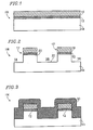
- Fig. 1 is a cross-sectional view of a device structure 10A obtained after the completion of the step of forming a first polysilicon layer 16, which may also be referred to as poly 1 throughout this description, according to a method of the present invention for producing a semiconductor device using a self-aligned shallow trench isolation process.
- a semiconductor substrate 14 e.g., a silicon substrate (Si substrate).
- An n-well or a p-well may be formed if desired prior to isolating adjacent device areas .
- a gate insulator 12 which is a gate insulating layer (e.g., a gate oxide film), is grown, or grown and deposited overlying the semiconductor substrate 14.
- Poly 1 is deposited overlying the gate insulator 12, following formation of n-wells or p-wells, if any.
- the device structure 10A is formed after the process of forming the sacrificial gate (the process of forming poly 1).
- the thickness of poly 1 is referred to as T p1 .
- a silicon nitride layer replaces, as a sacrificial gate material, the poly 1 overlying the gate insulator 12.
- the gate insulator 12 may comprise silicon oxide (e.g., silicon dioxide), or a high-k material, such as silicon oxynitride, hafnium oxide, zirconium oxide, lanthanum oxide or other suitable gate dielectric material.
- Fig. 2 is a cross-sectional view of a device structure 10B obtained after the completion of the step of forming trenches according to the method of the present invention for producing a semiconductor device using a self-aligned shallow trench isolation process.
- the poly 1, the gate insulator 12, and the semiconductor substrate 14 are partially etched to form trenches 18, thereby forming adjacent device regions 17.
- the device structure 10B is obtained after the process of forming the trenches.
- the tolerance (uncertainty or variation) in the trench depth is referred to as ⁇ X STI .
- a cleaning may be performed to reduce, or eliminate, etch damage.
- Fig. 3 is a cross-sectional view of a device structure 10C obtained after the completion of the step of forming an oxide layer according to the method of the present invention for producing a semiconductor device using a self-aligned shallow trench isolation process.
- an oxide layer 30 is deposited on the poly 1 and on the substrate 14 within the trenches 18, thereby obtaining the device structure 10C after the process of forming the oxide layer.
- the purpose of depositing the oxide layer 30 is to refill the trenches 18 with the oxide.
- the oxide layer 30 is formed so as to have a thickness greater than the depth of the trench. Specifically, the oxide layer 30 has a minimum thickness that is greater than the maximum possible depth of the trench 18 into the semiconductor substrate 14.
- the oxide layer 30 should be deposited and processed so that the final processed thickness satisfies the following expression (1): T OX - ⁇ T OX >X STI + ⁇ X STI
- the oxide layer 30 may comprise a thin thermal oxide to provide a good interface between the oxide and silicon in the field followed by a deposited oxide.
- the deposited oxide can be formed by a variety of film formation methods including chemical vapor deposition (CVD) methods, such as, LTO, HPCVD, PECVD, or other CVD methods. Non-CVD methods such as sputtering may also be used. Following deposition of oxide by any suitable film formation method, the oxide may then be densified at a higher temperature, if necessary or desired.
- CVD chemical vapor deposition
- Fig. 4 is a cross-sectional view of a device structure 10D obtained after the completion of the step of forming poly 2 according to the method of the present invention for producing a semiconductor device using a self-aligned shallow trench isolation process.
- a second polysilicon layer 40 also referred to herein as poly 2, or field poly, is deposited overlying the device structure 10C (or the oxide layer 30).
- the thickness of poly 2 is referred to as T p2
- the thickness of poly 1 (or the total thickness of poly 1 and the gate insulator 12) is referred to as T p1 .
- Poly 2 should have a thickness selected such that the maximum thickness of poly 2 plus the maximum thickness of the oxide layer 30 is thinner than the minimum depth of the trench 18 plus the minimum thickness of poly 1. Accordingly, the thickness of poly 2 should satisfy the following expression (2): T p2 + ⁇ T p2 +T OX + ⁇ T OX ⁇ X STI - ⁇ X STI +T p1 - ⁇ T p1
- the maximum desired thickness of the oxide layer 30 should satisfy the following expression (3): T OX + ⁇ T OX ⁇ X STI - ⁇ X STI +T p1 - ⁇ T p1 -T p2 - ⁇ T p2
- the device structure 10D is obtained after the process of forming poly 2.
- a sacrificial oxide layer is deposited overlying the device structure 10D.
- the sacrificial oxide layer may be, for example, undensified TEOS.
- the sacrificial oxide layer is one and a half times thicker than the maximum thickness of poly 1.
- the sacrificial oxide layer should have a thickness such that the combined thickness of the gate insulator 12, poly 1, the oxide layer 30, poly 2, and the sacrificial oxide layer is approximately two times the total step height of the active area features, which corresponds to the actual physical relief of the top surfaces.
- Fig. 5 is a cross-sectional view of a device structure 10E obtained after the completion of the planarization step according to the method of the present invention for producing a semiconductor device using a self-aligned shallow trench isolation process.
- poly 2 the second polysilicon layer 40
- the oxide layer 30 are partially polished by a low-selection-ratio CMP and then the resultant device structure is polished and planarized from the top surface thereof using a high-selection-ratio CMP to stop at the top surface of the second polysilicon layer 40 as a stopper in the field region.
- the device structure 10E is obtained after the planarization process.
- the planarization process may be achieved using the following two-step process. In the first step, a non-selective slurry is used to remove the overlying oxide and the portion of the second polysilicon layer 40 overlying active areas within the device regions.
- the second step utilizes a selective polish, which continues to remove the oxide layer 30 overlying the active area within the device regions and stops at the first polysilicon layer 16 overlying the active areas within the device regions and at the top surface of the second polysilicon layer 40 in the field regions.
- the actual field oxide (the oxide layer 30 in the field regions) is not polished in this planarization step.
- the active areas of the device are much smaller than the field areas and the polish rate of oxide can be selected to be sufficiently higher than that of polysilicon, for example, greater than 5:1 oxide to polysilicon etch ratio, so this CMP process can be readily achieved.
- any sacrificial gate material would be removed.
- the sacrificial gate material could be polysilicon, silicon nitride or other suitable sacrificial gate material.
- the underlying gate insulator may also be removed if desired.
- a replacement gate insulator for example a high-k gate insulator, maybe formed. A replacement gate process could then be completed.
- Fig. 6 is a cross-sectional view of a device structure 10F after the completion of the step of forming poly 3 according to the method of the present invention for producing a semiconductor device using a self-aligned shallow trench isolation process.
- a third polysilicon layer 60 is deposited overlying the device structure 10E planarized by CMP.
- the actual gate polysilicon thickness will correspond to the sum of the poly 3 thickness plus the thickness of poly 1 (the first polysilicon layer 16) that remains after CMP. In this manner, the device structure 10F is obtained after the process of forming poly 3.
- Fig. 7 is a cross-sectional view of a device structure 10G obtained after the completion of the step of forming a polysilicon gate according to the method of the present invention for producing a semiconductor device using a self-aligned shallow trench isolation process.
- photoresist 70 is applied to poly 3 (the third polysilicon layer 60) and patterned to define a polysilicon gate structure 72.
- a two-step plasma etch process may be used to etch the poly 3/poly 1 (the first polysilicon layer 16) stack and the poly 3/poly 2 (the second polysilicon layer 40) stack.
- the first step has a high polysilicon etch rate and stops at the end point, which corresponds to the point at which exposed poly 2 has been completely removed. Notice that some poly 2 remains under poly 3 and the photoresist. In this manner, the device structure 10G is obtained after the process of forming the polysilicon gate.
- Fig. 8 is a cross-sectional view of the device structure 10G shown in Fig. 7 rotated ninety degrees to show the cross-section along the source/channel/drain (a transistor region 15) of a transistor.
- poly 1 (the first polysilicon layer 16) is not completely removed from the active region (the transistor region 15), as shown in Fig. 8.
- the thickness of the remaining poly 1 should be independent of the CMP process.
- a highly selective etch is used to etch the remaining portion of poly 1 (the first polysilicon layer 16) that is not covered by photoresist.
- the highly selective etch stops at the bottom surface of poly 2 and leaves a thin layer 16A of poly 1 (the first polysilicon layer 16) over the gate insulator 12.
- Fig. 9 is a cross-sectional view of a device structure 10H illustrating the active region (the transistor region 15) including the source, channel, and drain regions after the completion of the step of removing the remaining poly 1 according to the method of the present invention for producing a semiconductor device using a self-aligned shallow trench isolation process.
- a highly selective etch is performed to remove the remaining thin layer 16A of poly 1, whereby micro-trenching may be reduced, or eliminated.
- the remainder of poly 1 the first polysilicon layer 16
- the remainder of poly 1 can be selectively and securely removed without excessive removal of gate insulator 12 in the source and drain regions.
- the photoresist 70 is then stripped leaving the polysilicon gate stack that comprises the remaining portions of poly 1 and poly 3 over each active area.
- Some poly 2 i.e., the portion of the second polysilicon layer 40 shown in Fig. 7 remains under the portion of poly 3 (the third polysilicon layer 60) extending beyond the active region (the transistor region 15), which is not visible in Fig. 9.
- the device structure 10H is obtained after the process of removing the remaining poly 1.
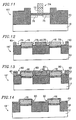
- Fig. 10 is a cross-sectional view of a device structure 10I obtained after the completion of the step of implanting impurity ions according to the method of the present invention for producing a semiconductor device using a self-aligned shallow trench isolation process.
- Fig. 11 is a cross-sectional view of the device structure 10I shown in Fig. 10 rotated ninety degrees to show the cross-section along the source/channel/drain (the transistor region 15) of a transistor.
- impurity ions are implanted into the semiconductor substrate 14 to form source and drain regions 76 that are self-aligned to the gate structure 72, as shown in Figs. 10 and 11.
- Poly 1, poly 2, and poly 3 are also converted to n+ or p+ polysilicon as is common in conventional processes.
- the polysilicon gate structure 72 may alternatively be doped prior to the gate electrode etch, and prior to (or during) implanting of impurity ions into portions of the semiconductor substrate 14 which correspond to the source and drain regions 76.
- the polysilicon gate may also be salicided. Several methods of polysilicon gate doping, silicide or self aligned processes, including salicide processes, may be applied to the present process.
- a polysilicon gate structure 72A following doping is shown in Fig. 10 and Fig. 11. In this manner, the device structure 10I is obtained after the process of implanting impurity ions.
- Each embodiments of the present invention may exhibit some, or all, of the advantages of modified STI processes, such as negligible narrow channel effects, high gate insulator integrity, uniform threshold voltage across the transistor, and low field leakage current.
- Fig. 12 illustrates a cross-sectional view of the device structure after an additional etch step is performed after the process leading up to the planarized structure shown in Fig. 5 above.
- an oxide etch is used to remove the exposed portion of the oxide layer 30.
- a plasma etch or a wet etch solution containing HF may be used to etch the oxide layer 30.
- the exposed portion of the oxide layer 30 is etched to remove approximately 100 nanometers of oxide forming recesses, i.e., notches 78 shown in Fig. 12. In this manner, a device structure 10E' is obtained after the process of etching the oxide is performed after the planarizing process described in conjunction with Fig. 5.
- the polysilicon layer 60 may be deposited over the device structure 10E', as shown in Fig. 13.
- the polysilicon layer 60 shown in Fig. 13 corresponds to poly 3 shown in Fig. 6, but with the addition of the alignment keys 80 to the portions corresponding to the notches 78.
- the process can then be completed as described above to form a final gate structure.
- the alignment keys 80 are now available for subsequent lithography alignment needs. In this manner, a device structure 10F' having an alignment structure is obtained after the process of forming poly 3 over the device structure 10E' shown in Fig. 12.
- alignment keys can be incorporated into a single poly STI structure using a modified STI process without poly 2.
- the resulting alignment structure with edges that serve as alignment keys 80 is shown in Fig. 14.
- the alignment keys 80 were formed by etching the oxide following CMP. After etching, another polysilicon layer corresponding to poly 3 is deposited. But in this case, there was no poly 2 used in the process. Subsequent processing may be used to complete the device structure to form a transistor with a gate, and source and drain regions. In this manner, a device structure 10F'' is obtained in the case where an alignment structure different from that shown in Fig. 13 is formed.
- an STI process of the present invention includes: a poly 1 formation step of forming the first polysilicon layer 16 overlying the semiconductor substrate 14; a trench formation step of forming the trench 18 (an element isolation trench) through the first polysilicon layer 16, and into the semiconductor substrate 14; an oxide layer formation step of filling the trench 18 with an oxide layer 30 such that the top surface of the oxide layer 30 within the trench 18 is higher than the bottom surface of the first polysilicon layer 16; a poly 2 formation step of depositing the second polysilicon layer 40 overlying the oxide layer 30 such that the top surface of the second polysilicon layer 40 within the trench 18 is lower than the top surface of the first polysilicon layer 16; a planarizing step of planarizing the second polysilicon layer 40, the oxide layer 30, and the first polysilicon layer 16 using a CMP process; an alignment key formation step of forming alignment keys by selectively etching the oxide layer 30; a poly 3 formation step of depositing the third polysilicon layer 60 over the planarized device structure; and a
- the second polysilicon layer 40 is deposited over the oxide layer 30 such that the bottom surface of the second polysilicon layer 40 within the trench 18 is above the bottom surface of the first polysilicon layer 16, and the top surface of the second polysilicon layer 40 within the trench 18 is below the top surface of the first polysilicon layer 16.
- the third polysilicon layer 60 is deposited over the second polysilicon layer 40 subjected to a planarization process. During forming the gate structure, an etch stop is detected at the completion of removal of each of the third polysilicon layer 60 and the second polysilicon layer 40. A thin layer of the remainder of the first polysilicon layer 16 is carefully removed using a highly selective etch process.
- the remainder of exposed first polysilicon layer 16 can be removed without excessive removal of the gate insulator layer 12 underlying the first polysilicon layer 16. Further, a bird's beak shift and dopant segregation in a well, which are caused in a LOCOS process, while solving the difficulty with end point detection of a gate polysilicon etch which is caused in the STI process, thereby preventing the formation of a parasitic edge transistor at a trench corner and a reduction of a gate withstand voltage.
- a second polysilicon layer is deposited over an oxide layer such that the bottom surface of the second polysilicon layer within a trench is above the bottom surface of the first polysilicon layer, and the top surface of the second polysilicon layer within the trench is below the top surface of the first polysilicon layer.
- a third polysilicon layer is deposited over the second polysilicon layer subjected to a planarization process. During forming a gate structure, an etch stop is detected at the completion of removal of each of the third polysilicon layer and the second polysilicon layer. A thin layer of the remainder of the first polysilicon layer is carefully removed using a highly selective etch process.
- the remainder of exposed first polysilicon layer can be removed without excessive removal of a gate insulator layer underlying the first polysilicon layer and the difficulty with end point detection of a gate polysilicon etch, which is caused in a conventional STI process , is solved, thereby preventing generation of a parasitic edge transistor at a trench corner and a reduction of a gate withstand voltage.
Landscapes
- Element Separation (AREA)
- Insulated Gate Type Field-Effect Transistor (AREA)
- Metal-Oxide And Bipolar Metal-Oxide Semiconductor Integrated Circuits (AREA)
Applications Claiming Priority (2)
| Application Number | Priority Date | Filing Date | Title |
|---|---|---|---|
| US112014 | 1993-08-25 | ||
| US10/112,014 US6627510B1 (en) | 2002-03-29 | 2002-03-29 | Method of making self-aligned shallow trench isolation |
Publications (3)
| Publication Number | Publication Date |
|---|---|
| EP1353369A2 true EP1353369A2 (fr) | 2003-10-15 |
| EP1353369A3 EP1353369A3 (fr) | 2004-05-06 |
| EP1353369B1 EP1353369B1 (fr) | 2007-12-12 |
Family
ID=28453218
Family Applications (1)
| Application Number | Title | Priority Date | Filing Date |
|---|---|---|---|
| EP03251430A Expired - Lifetime EP1353369B1 (fr) | 2002-03-29 | 2003-03-10 | Procédé de fabrication d'un dispositif semi-conducteur |
Country Status (6)
| Country | Link |
|---|---|
| US (1) | US6627510B1 (fr) |
| EP (1) | EP1353369B1 (fr) |
| KR (1) | KR100515181B1 (fr) |
| CN (1) | CN1278407C (fr) |
| DE (1) | DE60317963T2 (fr) |
| TW (1) | TWI235450B (fr) |
Families Citing this family (11)
| Publication number | Priority date | Publication date | Assignee | Title |
|---|---|---|---|---|
| JP5037766B2 (ja) * | 2001-09-10 | 2012-10-03 | ルネサスエレクトロニクス株式会社 | 半導体装置の製造方法 |
| DE10301291B3 (de) * | 2003-01-15 | 2004-08-26 | Infineon Technologies Ag | Verfahren zum Einbringen von eine unterschiedliche Dimensionierung aufweisenden Strukturen in ein Substrat |
| US6716691B1 (en) * | 2003-06-25 | 2004-04-06 | Sharp Laboratories Of America, Inc. | Self-aligned shallow trench isolation process having improved polysilicon gate thickness control |
| KR100514173B1 (ko) * | 2004-01-15 | 2005-09-09 | 삼성전자주식회사 | 반도체 장치의 게이트 형성 방법. |
| US7012021B2 (en) * | 2004-01-29 | 2006-03-14 | Taiwan Semiconductor Mfg | Method for end point detection polysilicon chemical mechanical polishing in an anti-fuse memory device |
| US8039339B2 (en) * | 2007-04-23 | 2011-10-18 | Freescale Semiconductor, Inc. | Separate layer formation in a semiconductor device |
| CN102468212B (zh) * | 2010-11-15 | 2014-03-12 | 中芯国际集成电路制造(上海)有限公司 | 浅沟槽隔离结构形成方法 |
| CN102339746B (zh) * | 2011-09-28 | 2016-04-06 | 上海华虹宏力半导体制造有限公司 | 形成平坦介质层的方法 |
| US9330959B2 (en) * | 2014-04-13 | 2016-05-03 | Texas Instruments Incorporated | Isolated semiconductor layer in bulk wafer by localized silicon epitaxial seed formation |
| US10811320B2 (en) * | 2017-09-29 | 2020-10-20 | Taiwan Semiconductor Manufacturing Company, Ltd. | Footing removal in cut-metal process |
| CN119767779A (zh) * | 2025-03-06 | 2025-04-04 | 合肥晶合集成电路股份有限公司 | 一种半导体器件的制备方法及半导体器件 |
Family Cites Families (22)
| Publication number | Priority date | Publication date | Assignee | Title |
|---|---|---|---|---|
| US5238859A (en) * | 1988-04-26 | 1993-08-24 | Kabushiki Kaisha Toshiba | Method of manufacturing semiconductor device |
| JPH0370180A (ja) * | 1989-08-09 | 1991-03-26 | Fujitsu Ltd | 半導体装置の製造方法 |
| US5202277A (en) * | 1989-12-08 | 1993-04-13 | Matsushita Electric Industrial Co., Ltd. | Method of fabricating a semiconductor device |
| JP3174786B2 (ja) * | 1991-05-31 | 2001-06-11 | 富士通株式会社 | 半導体装置の製造方法 |
| JP3057882B2 (ja) * | 1992-03-09 | 2000-07-04 | 日本電気株式会社 | 半導体装置の製造方法 |
| JP3202460B2 (ja) * | 1993-12-21 | 2001-08-27 | 株式会社東芝 | 半導体装置およびその製造方法 |
| US6069081A (en) * | 1995-04-28 | 2000-05-30 | International Buiness Machines Corporation | Two-step chemical mechanical polish surface planarization technique |
| JP2790084B2 (ja) * | 1995-08-16 | 1998-08-27 | 日本電気株式会社 | 半導体装置の製造方法 |
| DE19538005A1 (de) * | 1995-10-12 | 1997-04-17 | Fraunhofer Ges Forschung | Verfahren zum Erzeugen einer Grabenisolation in einem Substrat |
| US5665202A (en) * | 1995-11-24 | 1997-09-09 | Motorola, Inc. | Multi-step planarization process using polishing at two different pad pressures |
| US6091129A (en) * | 1996-06-19 | 2000-07-18 | Cypress Semiconductor Corporation | Self-aligned trench isolated structure |
| JPH10125637A (ja) * | 1996-10-15 | 1998-05-15 | Toshiba Corp | 半導体装置の製造方法 |
| US6103592A (en) * | 1997-05-01 | 2000-08-15 | International Business Machines Corp. | Manufacturing self-aligned polysilicon fet devices isolated with maskless shallow trench isolation and gate conductor fill technology with active devices and dummy doped regions formed in mesas |
| JP3519579B2 (ja) * | 1997-09-09 | 2004-04-19 | 株式会社ルネサステクノロジ | 半導体装置及びその製造方法 |
| WO1999046081A1 (fr) * | 1998-03-11 | 1999-09-16 | Strasbaugh | Procede et dispositif de polissage mecanique chimique a phases multiples |
| TW418459B (en) * | 1998-06-30 | 2001-01-11 | Fujitsu Ltd | Semiconductor device manufacturing method |
| US6146975A (en) * | 1998-07-10 | 2000-11-14 | Lucent Technologies Inc. | Shallow trench isolation |
| KR20010004309A (ko) * | 1999-06-28 | 2001-01-15 | 김영환 | 웨이퍼 정렬키 형성방법 |
| KR100318270B1 (ko) * | 1999-12-16 | 2001-12-24 | 박종섭 | 반도체 소자의 오버레이 버어니어 형성방법 |
| US6417072B2 (en) * | 2000-02-10 | 2002-07-09 | International Business Machines Corporation | Method of forming STI oxide regions and alignment marks in a semiconductor structure with one masking step |
| JP3503888B2 (ja) * | 2000-09-01 | 2004-03-08 | 沖電気工業株式会社 | アライメントマーク及びその形成方法 |
| US6713884B2 (en) * | 2001-12-20 | 2004-03-30 | Infineon Technologies Ag | Method of forming an alignment mark structure using standard process steps for forming vertical gate transistors |
-
2002
- 2002-03-29 US US10/112,014 patent/US6627510B1/en not_active Expired - Lifetime
-
2003
- 2003-01-23 TW TW092101505A patent/TWI235450B/zh not_active IP Right Cessation
- 2003-02-07 KR KR10-2003-0007697A patent/KR100515181B1/ko not_active Expired - Fee Related
- 2003-03-10 EP EP03251430A patent/EP1353369B1/fr not_active Expired - Lifetime
- 2003-03-10 DE DE60317963T patent/DE60317963T2/de not_active Expired - Lifetime
- 2003-03-18 CN CNB031216234A patent/CN1278407C/zh not_active Expired - Fee Related
Also Published As
| Publication number | Publication date |
|---|---|
| CN1457090A (zh) | 2003-11-19 |
| EP1353369B1 (fr) | 2007-12-12 |
| DE60317963D1 (de) | 2008-01-24 |
| TWI235450B (en) | 2005-07-01 |
| US6627510B1 (en) | 2003-09-30 |
| TW200304686A (en) | 2003-10-01 |
| DE60317963T2 (de) | 2008-11-27 |
| CN1278407C (zh) | 2006-10-04 |
| US20030186503A1 (en) | 2003-10-02 |
| EP1353369A3 (fr) | 2004-05-06 |
| KR100515181B1 (ko) | 2005-09-16 |
| KR20030078637A (ko) | 2003-10-08 |
Similar Documents
| Publication | Publication Date | Title |
|---|---|---|
| US6392271B1 (en) | Structure and process flow for fabrication of dual gate floating body integrated MOS transistors | |
| KR0165457B1 (ko) | 트렌치 소자분리 방법 | |
| EP1069613B1 (fr) | Architecture à faible fuite pour dispositif CMOS sub-0.18-micrométriques en siliciure | |
| US20060006462A1 (en) | Method and apparatus for a semiconductor device having low and high voltage transistors | |
| EP1213757A2 (fr) | Circuits intégrés et régions adjacentes p-dopées avec des structures d'isolation par tranchées peu profondes sans revêtement du type "Liner" et méthodes de fabrication | |
| US8546268B2 (en) | Manufacturing integrated circuit components having multiple gate oxidations | |
| KR20020044541A (ko) | 전자 구조물 및 이의 형성 방법 | |
| US6716691B1 (en) | Self-aligned shallow trench isolation process having improved polysilicon gate thickness control | |
| US6355540B2 (en) | Stress-free shallow trench isolation | |
| EP1353369B1 (fr) | Procédé de fabrication d'un dispositif semi-conducteur | |
| US7378306B2 (en) | Selective silicon deposition for planarized dual surface orientation integration | |
| US6858514B2 (en) | Low power flash memory cell and method | |
| US6248641B1 (en) | Method of fabricating shallow trench isolation | |
| US7678664B2 (en) | Method for fabricating semiconductor device | |
| US6306741B1 (en) | Method of patterning gate electrodes with high K gate dielectrics | |
| JP2007096310A (ja) | 半導体装置の製造方法 | |
| JP2004296754A (ja) | 半導体装置および半導体装置の製造方法 | |
| KR100466207B1 (ko) | 반도체 소자의 제조 방법 | |
| JP3567773B2 (ja) | トレンチ素子分離領域を有する半導体装置の製造方法 | |
| US6773975B1 (en) | Formation of a shallow trench isolation structure in integrated circuits | |
| US6303461B1 (en) | Method for fabricating a shallow trench isolation structure | |
| US9349654B2 (en) | Isolation for embedded devices | |
| JP4989076B2 (ja) | 半導体装置の製造方法 | |
| JP2004228545A (ja) | 半導体装置の製造方法 | |
| JPH1050822A (ja) | 半導体装置の製造方法 |
Legal Events
| Date | Code | Title | Description |
|---|---|---|---|
| PUAI | Public reference made under article 153(3) epc to a published international application that has entered the european phase |
Free format text: ORIGINAL CODE: 0009012 |
|
| AK | Designated contracting states |
Kind code of ref document: A2 Designated state(s): AT BE BG CH CY CZ DE DK EE ES FI FR GB GR HU IE IT LI LU MC NL PT RO SE SI SK TR |
|
| AX | Request for extension of the european patent |
Extension state: AL LT LV MK RO |
|
| PUAL | Search report despatched |
Free format text: ORIGINAL CODE: 0009013 |
|
| AK | Designated contracting states |
Kind code of ref document: A3 Designated state(s): AT BE BG CH CY CZ DE DK EE ES FI FR GB GR HU IE IT LI LU MC NL PT RO SE SI SK TR |
|
| AX | Request for extension of the european patent |
Extension state: AL LT LV MK RO |
|
| 17P | Request for examination filed |
Effective date: 20041104 |
|
| 17Q | First examination report despatched |
Effective date: 20041201 |
|
| AKX | Designation fees paid |
Designated state(s): DE FR GB |
|
| GRAP | Despatch of communication of intention to grant a patent |
Free format text: ORIGINAL CODE: EPIDOSNIGR1 |
|
| GRAS | Grant fee paid |
Free format text: ORIGINAL CODE: EPIDOSNIGR3 |
|
| GRAA | (expected) grant |
Free format text: ORIGINAL CODE: 0009210 |
|
| AK | Designated contracting states |
Kind code of ref document: B1 Designated state(s): DE FR GB |
|
| REG | Reference to a national code |
Ref country code: GB Ref legal event code: FG4D |
|
| REF | Corresponds to: |
Ref document number: 60317963 Country of ref document: DE Date of ref document: 20080124 Kind code of ref document: P |
|
| ET | Fr: translation filed | ||
| PLBE | No opposition filed within time limit |
Free format text: ORIGINAL CODE: 0009261 |
|
| STAA | Information on the status of an ep patent application or granted ep patent |
Free format text: STATUS: NO OPPOSITION FILED WITHIN TIME LIMIT |
|
| 26N | No opposition filed |
Effective date: 20080915 |
|
| PGFP | Annual fee paid to national office [announced via postgrant information from national office to epo] |
Ref country code: FR Payment date: 20140311 Year of fee payment: 12 |
|
| PGFP | Annual fee paid to national office [announced via postgrant information from national office to epo] |
Ref country code: GB Payment date: 20140305 Year of fee payment: 12 |
|
| PGFP | Annual fee paid to national office [announced via postgrant information from national office to epo] |
Ref country code: DE Payment date: 20140417 Year of fee payment: 12 |
|
| REG | Reference to a national code |
Ref country code: DE Ref legal event code: R119 Ref document number: 60317963 Country of ref document: DE |
|
| GBPC | Gb: european patent ceased through non-payment of renewal fee |
Effective date: 20150310 |
|
| REG | Reference to a national code |
Ref country code: FR Ref legal event code: ST Effective date: 20151130 |
|
| PG25 | Lapsed in a contracting state [announced via postgrant information from national office to epo] |
Ref country code: DE Free format text: LAPSE BECAUSE OF NON-PAYMENT OF DUE FEES Effective date: 20151001 Ref country code: GB Free format text: LAPSE BECAUSE OF NON-PAYMENT OF DUE FEES Effective date: 20150310 |
|
| PG25 | Lapsed in a contracting state [announced via postgrant information from national office to epo] |
Ref country code: FR Free format text: LAPSE BECAUSE OF NON-PAYMENT OF DUE FEES Effective date: 20150331 |