EP1355187A1 - Verfahren zum Verbinden einer Leiterplatte mit einer Flüsigkristallanzeige - Google Patents
Verfahren zum Verbinden einer Leiterplatte mit einer Flüsigkristallanzeige Download PDFInfo
- Publication number
- EP1355187A1 EP1355187A1 EP02076554A EP02076554A EP1355187A1 EP 1355187 A1 EP1355187 A1 EP 1355187A1 EP 02076554 A EP02076554 A EP 02076554A EP 02076554 A EP02076554 A EP 02076554A EP 1355187 A1 EP1355187 A1 EP 1355187A1
- Authority
- EP
- European Patent Office
- Prior art keywords
- upper glass
- lcd
- pcb
- connection
- liquid crystal
- Prior art date
- Legal status (The legal status is an assumption and is not a legal conclusion. Google has not performed a legal analysis and makes no representation as to the accuracy of the status listed.)
- Granted
Links
- 238000000034 method Methods 0.000 title claims abstract description 16
- 239000004973 liquid crystal related substance Substances 0.000 title claims abstract description 13
- 239000011521 glass Substances 0.000 claims abstract description 29
- 239000000463 material Substances 0.000 claims abstract description 7
- 238000007789 sealing Methods 0.000 claims abstract description 5
- 238000009304 pastoral farming Methods 0.000 claims abstract description 4
- 210000004027 cell Anatomy 0.000 abstract 3
- 230000015572 biosynthetic process Effects 0.000 abstract 1
- 210000002858 crystal cell Anatomy 0.000 abstract 1
- SXHLTVKPNQVZGL-UHFFFAOYSA-N 1,2-dichloro-3-(3-chlorophenyl)benzene Chemical compound ClC1=CC=CC(C=2C(=C(Cl)C=CC=2)Cl)=C1 SXHLTVKPNQVZGL-UHFFFAOYSA-N 0.000 description 2
- 241000283070 Equus zebra Species 0.000 description 2
- 239000000853 adhesive Substances 0.000 description 2
- 230000001070 adhesive effect Effects 0.000 description 2
- 239000004020 conductor Substances 0.000 description 1
- 238000010276 construction Methods 0.000 description 1
- 239000012467 final product Substances 0.000 description 1
- 239000011888 foil Substances 0.000 description 1
- 235000015243 ice cream Nutrition 0.000 description 1
- 239000011159 matrix material Substances 0.000 description 1
- 239000000047 product Substances 0.000 description 1
- 239000010453 quartz Substances 0.000 description 1
- VYPSYNLAJGMNEJ-UHFFFAOYSA-N silicon dioxide Inorganic materials O=[Si]=O VYPSYNLAJGMNEJ-UHFFFAOYSA-N 0.000 description 1
- 239000000758 substrate Substances 0.000 description 1
- 238000003466 welding Methods 0.000 description 1
Images
Classifications
-
- G—PHYSICS
- G02—OPTICS
- G02F—OPTICAL DEVICES OR ARRANGEMENTS FOR THE CONTROL OF LIGHT BY MODIFICATION OF THE OPTICAL PROPERTIES OF THE MEDIA OF THE ELEMENTS INVOLVED THEREIN; NON-LINEAR OPTICS; FREQUENCY-CHANGING OF LIGHT; OPTICAL LOGIC ELEMENTS; OPTICAL ANALOGUE/DIGITAL CONVERTERS
- G02F1/00—Devices or arrangements for the control of the intensity, colour, phase, polarisation or direction of light arriving from an independent light source, e.g. switching, gating or modulating; Non-linear optics
- G02F1/01—Devices or arrangements for the control of the intensity, colour, phase, polarisation or direction of light arriving from an independent light source, e.g. switching, gating or modulating; Non-linear optics for the control of the intensity, phase, polarisation or colour
- G02F1/13—Devices or arrangements for the control of the intensity, colour, phase, polarisation or direction of light arriving from an independent light source, e.g. switching, gating or modulating; Non-linear optics for the control of the intensity, phase, polarisation or colour based on liquid crystals, e.g. single liquid crystal display cells
- G02F1/133—Constructional arrangements; Operation of liquid crystal cells; Circuit arrangements
- G02F1/1333—Constructional arrangements; Manufacturing methods
- G02F1/1345—Conductors connecting electrodes to cell terminals
- G02F1/13452—Conductors connecting driver circuitry and terminals of panels
-
- H—ELECTRICITY
- H05—ELECTRIC TECHNIQUES NOT OTHERWISE PROVIDED FOR
- H05K—PRINTED CIRCUITS; CASINGS OR CONSTRUCTIONAL DETAILS OF ELECTRIC APPARATUS; MANUFACTURE OF ASSEMBLAGES OF ELECTRICAL COMPONENTS
- H05K3/00—Apparatus or processes for manufacturing printed circuits
- H05K3/36—Assembling printed circuits with other printed circuits
- H05K3/361—Assembling flexible printed circuits with other printed circuits
-
- H—ELECTRICITY
- H01—ELECTRIC ELEMENTS
- H01R—ELECTRICALLY-CONDUCTIVE CONNECTIONS; STRUCTURAL ASSOCIATIONS OF A PLURALITY OF MUTUALLY-INSULATED ELECTRICAL CONNECTING ELEMENTS; COUPLING DEVICES; CURRENT COLLECTORS
- H01R12/00—Structural associations of a plurality of mutually-insulated electrical connecting elements, specially adapted for printed circuits, e.g. printed circuit boards [PCB], flat or ribbon cables, or like generally planar structures, e.g. terminal strips, terminal blocks; Coupling devices specially adapted for printed circuits, flat or ribbon cables, or like generally planar structures; Terminals specially adapted for contact with, or insertion into, printed circuits, flat or ribbon cables, or like generally planar structures
- H01R12/70—Coupling devices
- H01R12/7076—Coupling devices for connection between PCB and component, e.g. display
-
- H—ELECTRICITY
- H01—ELECTRIC ELEMENTS
- H01R—ELECTRICALLY-CONDUCTIVE CONNECTIONS; STRUCTURAL ASSOCIATIONS OF A PLURALITY OF MUTUALLY-INSULATED ELECTRICAL CONNECTING ELEMENTS; COUPLING DEVICES; CURRENT COLLECTORS
- H01R4/00—Electrically-conductive connections between two or more conductive members in direct contact, i.e. touching one another; Means for effecting or maintaining such contact; Electrically-conductive connections having two or more spaced connecting locations for conductors and using contact members penetrating insulation
- H01R4/02—Soldered or welded connections
-
- H—ELECTRICITY
- H05—ELECTRIC TECHNIQUES NOT OTHERWISE PROVIDED FOR
- H05K—PRINTED CIRCUITS; CASINGS OR CONSTRUCTIONAL DETAILS OF ELECTRIC APPARATUS; MANUFACTURE OF ASSEMBLAGES OF ELECTRICAL COMPONENTS
- H05K2201/00—Indexing scheme relating to printed circuits covered by H05K1/00
- H05K2201/01—Dielectrics
- H05K2201/0104—Properties and characteristics in general
- H05K2201/0108—Transparent
-
- H—ELECTRICITY
- H05—ELECTRIC TECHNIQUES NOT OTHERWISE PROVIDED FOR
- H05K—PRINTED CIRCUITS; CASINGS OR CONSTRUCTIONAL DETAILS OF ELECTRIC APPARATUS; MANUFACTURE OF ASSEMBLAGES OF ELECTRICAL COMPONENTS
- H05K2203/00—Indexing scheme relating to apparatus or processes for manufacturing printed circuits covered by H05K3/00
- H05K2203/10—Using electric, magnetic and electromagnetic fields; Using laser light
- H05K2203/107—Using laser light
Definitions
- the present invention relates to a method of connecting a display to liquid crystals on a printed circuit, in particular the printed circuit supporting the electronic components of a digital display, especially in a room watchmaking.
- a liquid crystal display comprises in a known manner, outside the sealing frame of two transparent substrates of the same dimension, tracks for connecting the display electrodes to a circuit to a circuit printed (PCB) having to the best knowledge of the applicant always a substantially flat surface.
- This connection is currently made using a "Zebra" type multitrack connector by welding, or by using an adhesive anisotropic conductor, or an ACF strip (Anisotropy Contacting Foil).
- Such processes are technically entirely satisfactory when the LCD and PCB are in the same plane.
- the present invention therefore relates to a new connection method from an LCD to a PCB, faster, more economical and technically more reliable in this that it does not use intermediate materials, but uses a laser beam.
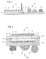
- a cell liquid crystal display (LCD) 10 connected according to the method of the invention to a printed circuit 20 (PCB) can be made of a flexible material.
- the cell usually comprises an upper glass 1 at the front of which is placed a polarizer 2, a lower lens 3, at the rear of which is placed a reflector 4, and a sealing frame 5 delimiting the liquid crystal confinement space (not visible in the figure in which the proportions in thickness have substantially been respected).
- the upper glass 1 has an extension 7 supporting on its lower surface the tracks of the electrodes.
- a printed circuit 20, supporting as electronic component for example a capa 12, a chip 14 and a quartz 16, is positioned under said extension 7, facing tracks the contact areas of the PCB to create a connection area 6 ..
- FIG. 2 relates to a second embodiment in which the PCB is positioned under the LCD.
- the LCD display cell 10 is comparable to that described in Figure 1, but the upper glass 1 has two extensions 7 and 9 which will establish two connection zones with the underlying PCB 20.
- the PCB 20 has a recess 19, which allows to accommodate the glass lower 3 and the reflector 4, so that the edges of this obviously come flush with the lower surfaces of the extensions 7, 9 supporting the tracks of the electrodes.
- the bottom of the recess 19 is lined with an adhesive 18 allowing to perform a pre-assembly, without using for example a assembly matrix. With this construction it is possible to focus the beam laser 30 in grazing incidence on the connection areas 6.8.
- the second embodiment allows to apply the method according to the invention to a display comprising several cells superimposed simply by staggering the connection areas in steps.
Landscapes
- Physics & Mathematics (AREA)
- Engineering & Computer Science (AREA)
- Nonlinear Science (AREA)
- General Physics & Mathematics (AREA)
- Mathematical Physics (AREA)
- Chemical & Material Sciences (AREA)
- Crystallography & Structural Chemistry (AREA)
- Microelectronics & Electronic Packaging (AREA)
- Manufacturing & Machinery (AREA)
- Optics & Photonics (AREA)
- Liquid Crystal (AREA)
- Devices For Indicating Variable Information By Combining Individual Elements (AREA)
- Electric Clocks (AREA)
- Wire Bonding (AREA)
- Coupling Device And Connection With Printed Circuit (AREA)
- Combinations Of Printed Boards (AREA)
Priority Applications (6)
| Application Number | Priority Date | Filing Date | Title |
|---|---|---|---|
| AT02076554T ATE499629T1 (de) | 2002-04-19 | 2002-04-19 | Verfahren zum verbinden einer leiterplatte mit einer flüssigkristallanzeige |
| EP02076554A EP1355187B1 (de) | 2002-04-19 | 2002-04-19 | Verfahren zum Verbinden einer Leiterplatte mit einer Flüssigkristallanzeige |
| DE60239261T DE60239261D1 (de) | 2002-04-19 | 2002-04-19 | Verfahren zum Verbinden einer Leiterplatte mit einer Flüssigkristallanzeige |
| US10/403,035 US6770837B2 (en) | 2002-04-19 | 2003-04-01 | Method for connecting a printed circuit to a liquid crystal display |
| JP2003106300A JP4464065B2 (ja) | 2002-04-19 | 2003-04-10 | 液晶ディスプレイにプリント回路を接続する方法 |
| HK04102237.5A HK1059827B (en) | 2004-03-25 | Process for connection of a printed circuit board to a liquid crystal display |
Applications Claiming Priority (1)
| Application Number | Priority Date | Filing Date | Title |
|---|---|---|---|
| EP02076554A EP1355187B1 (de) | 2002-04-19 | 2002-04-19 | Verfahren zum Verbinden einer Leiterplatte mit einer Flüssigkristallanzeige |
Publications (2)
| Publication Number | Publication Date |
|---|---|
| EP1355187A1 true EP1355187A1 (de) | 2003-10-22 |
| EP1355187B1 EP1355187B1 (de) | 2011-02-23 |
Family
ID=28459557
Family Applications (1)
| Application Number | Title | Priority Date | Filing Date |
|---|---|---|---|
| EP02076554A Expired - Lifetime EP1355187B1 (de) | 2002-04-19 | 2002-04-19 | Verfahren zum Verbinden einer Leiterplatte mit einer Flüssigkristallanzeige |
Country Status (5)
| Country | Link |
|---|---|
| US (1) | US6770837B2 (de) |
| EP (1) | EP1355187B1 (de) |
| JP (1) | JP4464065B2 (de) |
| AT (1) | ATE499629T1 (de) |
| DE (1) | DE60239261D1 (de) |
Families Citing this family (1)
| Publication number | Priority date | Publication date | Assignee | Title |
|---|---|---|---|---|
| FI123860B (fi) | 2010-05-18 | 2013-11-29 | Corelase Oy | Menetelmä substraattien tiivistämiseksi ja kontaktoimiseksi laservalon avulla ja elektroniikkamoduli |
Citations (4)
| Publication number | Priority date | Publication date | Assignee | Title |
|---|---|---|---|---|
| US4654965A (en) * | 1984-07-16 | 1987-04-07 | Ricoh Company, Ltd. | Method of manufacturing liquid crystal display unit |
| JPS63241523A (ja) * | 1987-03-30 | 1988-10-06 | Toshiba Corp | 液晶パネル基板装置 |
| US4836651A (en) * | 1987-12-03 | 1989-06-06 | Anderson Richard A | Flexible circuit interconnection for a matrix addressed liquid crystal panel |
| US5606440A (en) * | 1992-04-30 | 1997-02-25 | Sharp Kabushiki Kaisha | Assembling method of flat type display device |
Family Cites Families (6)
| Publication number | Priority date | Publication date | Assignee | Title |
|---|---|---|---|---|
| JPH0820638B2 (ja) * | 1986-08-08 | 1996-03-04 | 株式会社半導体エネルギ−研究所 | 液晶装置およびその作製方法 |
| US5102361A (en) * | 1989-01-23 | 1992-04-07 | Sharp Kabushiki Kaisha | Method for the manufacture of active matrix display apparatuses |
| TW305948B (de) * | 1993-11-08 | 1997-05-21 | Hitachi Ltd | |
| JP4498489B2 (ja) * | 1999-03-19 | 2010-07-07 | シャープ株式会社 | 液晶表示装置とその製造方法 |
| JP4001712B2 (ja) * | 2000-03-29 | 2007-10-31 | シャープ株式会社 | 液晶表示装置の欠陥修復方法 |
| JP2002196352A (ja) * | 2000-12-07 | 2002-07-12 | Koninkl Philips Electronics Nv | 予備配線を有する液晶表示装置 |
-
2002
- 2002-04-19 AT AT02076554T patent/ATE499629T1/de not_active IP Right Cessation
- 2002-04-19 DE DE60239261T patent/DE60239261D1/de not_active Expired - Lifetime
- 2002-04-19 EP EP02076554A patent/EP1355187B1/de not_active Expired - Lifetime
-
2003
- 2003-04-01 US US10/403,035 patent/US6770837B2/en not_active Expired - Lifetime
- 2003-04-10 JP JP2003106300A patent/JP4464065B2/ja not_active Expired - Fee Related
Patent Citations (4)
| Publication number | Priority date | Publication date | Assignee | Title |
|---|---|---|---|---|
| US4654965A (en) * | 1984-07-16 | 1987-04-07 | Ricoh Company, Ltd. | Method of manufacturing liquid crystal display unit |
| JPS63241523A (ja) * | 1987-03-30 | 1988-10-06 | Toshiba Corp | 液晶パネル基板装置 |
| US4836651A (en) * | 1987-12-03 | 1989-06-06 | Anderson Richard A | Flexible circuit interconnection for a matrix addressed liquid crystal panel |
| US5606440A (en) * | 1992-04-30 | 1997-02-25 | Sharp Kabushiki Kaisha | Assembling method of flat type display device |
Non-Patent Citations (2)
| Title |
|---|
| "COMPACT LIQUID CRYSTAL DISPLAY MODULE STRUCTURE", IBM TECHNICAL DISCLOSURE BULLETIN, IBM CORP. NEW YORK, US, vol. 40, no. 2, 1 February 1997 (1997-02-01), pages 227 - 228, XP000692230, ISSN: 0018-8689 * |
| PATENT ABSTRACTS OF JAPAN vol. 013, no. 047 (P - 822) 3 February 1989 (1989-02-03) * |
Also Published As
| Publication number | Publication date |
|---|---|
| ATE499629T1 (de) | 2011-03-15 |
| US6770837B2 (en) | 2004-08-03 |
| HK1059827A1 (en) | 2004-07-16 |
| US20030197827A1 (en) | 2003-10-23 |
| JP4464065B2 (ja) | 2010-05-19 |
| DE60239261D1 (de) | 2011-04-07 |
| JP2003315823A (ja) | 2003-11-06 |
| EP1355187B1 (de) | 2011-02-23 |
Similar Documents
| Publication | Publication Date | Title |
|---|---|---|
| FR2594992A1 (fr) | Dispositif d'affichage a cristal liquide | |
| EP3650958B1 (de) | Gegenstand, der mit einer elektrooptischen anzeigevorrichtung ausgestattet ist | |
| FR2482344A1 (fr) | Afficheur bidimensionnel a couche fluide commandee electriquement et son procede de fabrication | |
| EP1780616A3 (de) | Anzeigeanordnung mit dekorativen Effekten für ein tragbares Instrument, wie eine Uhr | |
| EP0324700A1 (de) | Gehäuse zur Umhüllung eines zerbrechlichen Elementes, wie einer logischen Schaltung und Verfahren zur Montage eines derartigen Gehäuses | |
| EP2477084A1 (de) | Armbanduhr mit einem elastomeren Anschluss für die elektrische Verbindung eines digitalen Anzeigegeräts mit einer Leiterplatte, und Verfahren für den Zusammenbau einer solchen Uhr | |
| EP1734423B1 (de) | Montage eines Sensorglases in einem Gehäuse | |
| EP1355187B1 (de) | Verfahren zum Verbinden einer Leiterplatte mit einer Flüssigkristallanzeige | |
| FR2762115A1 (fr) | Procede d'insertion d'un module electronique dans un corps de carte a memoire electronique | |
| EP2584413B1 (de) | Vorrichtung zum Befestigen eines Glases auf einem Mittelteil eines Armbanduhrgehäuses | |
| FR2987169A1 (fr) | Procede de liaison d'un premier composant electronique a un deuxieme composant | |
| FR2844606A1 (fr) | Miroir electrochrome, et couche reflechissante pour ledit miroir | |
| EP0828413B1 (de) | Elektro-optische Anzeigeeinrichtung und flexibler Träger für solche Einrichtungen zur Stromversorgung dieser Einrichtungen | |
| EP2673676B1 (de) | Uhr mit einer einfassung und verfahren zur anbringung einer solchen einfassung | |
| EP1055149B1 (de) | Elektrooptische zelle oder elektrochemische photovoltaische zelle und verfahren zu ihrer herstellung | |
| EP1734422A1 (de) | Zusammenbau eines Glases auf ein berührungsempfindliches Gehäuse | |
| EP2732318B1 (de) | Lichtleiter zur beleuchtung einer anzeigevorrichtung | |
| EP2447790A1 (de) | Glas für die obere Abdeckung des Gehäuses eines tragbaren Gegenstands | |
| FR2637110A1 (fr) | Cellule electro-optique perfectionnee | |
| CH704453A2 (fr) | Montre comprenant une lunette et procédé de fixation d'une telle lunette. | |
| CH703966A2 (fr) | Glace servant à fermer par le haut la boîte d'un objet portable. | |
| CH722082A1 (fr) | Dispositif horloger assurant une étanchéité à grande profondeur | |
| CH703289B1 (fr) | Dispositif d'encapsulage pour MEMS. | |
| FR2817398A1 (fr) | Boitier en film ultra-mince | |
| CH705659A2 (fr) | Procédé de fixation d'une glace sur une carrure d'une boîte de montre. |
Legal Events
| Date | Code | Title | Description |
|---|---|---|---|
| PUAI | Public reference made under article 153(3) epc to a published international application that has entered the european phase |
Free format text: ORIGINAL CODE: 0009012 |
|
| AK | Designated contracting states |
Kind code of ref document: A1 Designated state(s): AT BE CH CY DE DK ES FI FR GB GR IE IT LI LU MC NL PT SE TR |
|
| AX | Request for extension of the european patent |
Extension state: AL LT LV MK RO SI |
|
| 17P | Request for examination filed |
Effective date: 20040422 |
|
| 17Q | First examination report despatched |
Effective date: 20040524 |
|
| AKX | Designation fees paid |
Designated state(s): AT BE CH CY DE DK ES FI FR GB GR IE IT LI LU MC NL PT SE TR |
|
| REG | Reference to a national code |
Ref country code: HK Ref legal event code: DE Ref document number: 1059827 Country of ref document: HK |
|
| GRAP | Despatch of communication of intention to grant a patent |
Free format text: ORIGINAL CODE: EPIDOSNIGR1 |
|
| GRAS | Grant fee paid |
Free format text: ORIGINAL CODE: EPIDOSNIGR3 |
|
| GRAA | (expected) grant |
Free format text: ORIGINAL CODE: 0009210 |
|
| AK | Designated contracting states |
Kind code of ref document: B1 Designated state(s): AT BE CH CY DE DK ES FI FR GB GR IE IT LI LU MC NL PT SE TR |
|
| REG | Reference to a national code |
Ref country code: GB Ref legal event code: FG4D Free format text: NOT ENGLISH |
|
| REG | Reference to a national code |
Ref country code: CH Ref legal event code: EP Ref country code: CH Ref legal event code: NV Representative=s name: ICB INGENIEURS CONSEILS EN BREVETS SA |
|
| REG | Reference to a national code |
Ref country code: IE Ref legal event code: FG4D Free format text: LANGUAGE OF EP DOCUMENT: FRENCH |
|
| REF | Corresponds to: |
Ref document number: 60239261 Country of ref document: DE Date of ref document: 20110407 Kind code of ref document: P |
|
| REG | Reference to a national code |
Ref country code: DE Ref legal event code: R096 Ref document number: 60239261 Country of ref document: DE Effective date: 20110407 |
|
| REG | Reference to a national code |
Ref country code: HK Ref legal event code: GR Ref document number: 1059827 Country of ref document: HK |
|
| REG | Reference to a national code |
Ref country code: NL Ref legal event code: VDEP Effective date: 20110223 |
|
| PG25 | Lapsed in a contracting state [announced via postgrant information from national office to epo] |
Ref country code: GR Free format text: LAPSE BECAUSE OF FAILURE TO SUBMIT A TRANSLATION OF THE DESCRIPTION OR TO PAY THE FEE WITHIN THE PRESCRIBED TIME-LIMIT Effective date: 20110524 Ref country code: SE Free format text: LAPSE BECAUSE OF FAILURE TO SUBMIT A TRANSLATION OF THE DESCRIPTION OR TO PAY THE FEE WITHIN THE PRESCRIBED TIME-LIMIT Effective date: 20110223 Ref country code: PT Free format text: LAPSE BECAUSE OF FAILURE TO SUBMIT A TRANSLATION OF THE DESCRIPTION OR TO PAY THE FEE WITHIN THE PRESCRIBED TIME-LIMIT Effective date: 20110623 Ref country code: ES Free format text: LAPSE BECAUSE OF FAILURE TO SUBMIT A TRANSLATION OF THE DESCRIPTION OR TO PAY THE FEE WITHIN THE PRESCRIBED TIME-LIMIT Effective date: 20110603 |
|
| PG25 | Lapsed in a contracting state [announced via postgrant information from national office to epo] |
Ref country code: NL Free format text: LAPSE BECAUSE OF FAILURE TO SUBMIT A TRANSLATION OF THE DESCRIPTION OR TO PAY THE FEE WITHIN THE PRESCRIBED TIME-LIMIT Effective date: 20110223 Ref country code: CY Free format text: LAPSE BECAUSE OF FAILURE TO SUBMIT A TRANSLATION OF THE DESCRIPTION OR TO PAY THE FEE WITHIN THE PRESCRIBED TIME-LIMIT Effective date: 20110223 Ref country code: AT Free format text: LAPSE BECAUSE OF FAILURE TO SUBMIT A TRANSLATION OF THE DESCRIPTION OR TO PAY THE FEE WITHIN THE PRESCRIBED TIME-LIMIT Effective date: 20110223 Ref country code: FI Free format text: LAPSE BECAUSE OF FAILURE TO SUBMIT A TRANSLATION OF THE DESCRIPTION OR TO PAY THE FEE WITHIN THE PRESCRIBED TIME-LIMIT Effective date: 20110223 |
|
| REG | Reference to a national code |
Ref country code: IE Ref legal event code: FD4D |
|
| BERE | Be: lapsed |
Owner name: ETA SA MANUFACTURE HORLOGERE SUISSE Effective date: 20110430 |
|
| PG25 | Lapsed in a contracting state [announced via postgrant information from national office to epo] |
Ref country code: DK Free format text: LAPSE BECAUSE OF FAILURE TO SUBMIT A TRANSLATION OF THE DESCRIPTION OR TO PAY THE FEE WITHIN THE PRESCRIBED TIME-LIMIT Effective date: 20110223 Ref country code: IE Free format text: LAPSE BECAUSE OF FAILURE TO SUBMIT A TRANSLATION OF THE DESCRIPTION OR TO PAY THE FEE WITHIN THE PRESCRIBED TIME-LIMIT Effective date: 20110223 |
|
| PG25 | Lapsed in a contracting state [announced via postgrant information from national office to epo] |
Ref country code: MC Free format text: LAPSE BECAUSE OF NON-PAYMENT OF DUE FEES Effective date: 20110430 |
|
| PLBE | No opposition filed within time limit |
Free format text: ORIGINAL CODE: 0009261 |
|
| STAA | Information on the status of an ep patent application or granted ep patent |
Free format text: STATUS: NO OPPOSITION FILED WITHIN TIME LIMIT |
|
| GBPC | Gb: european patent ceased through non-payment of renewal fee |
Effective date: 20110523 |
|
| PG25 | Lapsed in a contracting state [announced via postgrant information from national office to epo] |
Ref country code: BE Free format text: LAPSE BECAUSE OF NON-PAYMENT OF DUE FEES Effective date: 20110430 |
|
| 26N | No opposition filed |
Effective date: 20111124 |
|
| REG | Reference to a national code |
Ref country code: DE Ref legal event code: R097 Ref document number: 60239261 Country of ref document: DE Effective date: 20111124 |
|
| PG25 | Lapsed in a contracting state [announced via postgrant information from national office to epo] |
Ref country code: IT Free format text: LAPSE BECAUSE OF FAILURE TO SUBMIT A TRANSLATION OF THE DESCRIPTION OR TO PAY THE FEE WITHIN THE PRESCRIBED TIME-LIMIT Effective date: 20110223 |
|
| PG25 | Lapsed in a contracting state [announced via postgrant information from national office to epo] |
Ref country code: GB Free format text: LAPSE BECAUSE OF NON-PAYMENT OF DUE FEES Effective date: 20110523 |
|
| PG25 | Lapsed in a contracting state [announced via postgrant information from national office to epo] |
Ref country code: LU Free format text: LAPSE BECAUSE OF NON-PAYMENT OF DUE FEES Effective date: 20110419 |
|
| PGFP | Annual fee paid to national office [announced via postgrant information from national office to epo] |
Ref country code: DE Payment date: 20130322 Year of fee payment: 12 |
|
| PGFP | Annual fee paid to national office [announced via postgrant information from national office to epo] |
Ref country code: FR Payment date: 20130603 Year of fee payment: 12 |
|
| PG25 | Lapsed in a contracting state [announced via postgrant information from national office to epo] |
Ref country code: TR Free format text: LAPSE BECAUSE OF FAILURE TO SUBMIT A TRANSLATION OF THE DESCRIPTION OR TO PAY THE FEE WITHIN THE PRESCRIBED TIME-LIMIT Effective date: 20110223 |
|
| REG | Reference to a national code |
Ref country code: DE Ref legal event code: R119 Ref document number: 60239261 Country of ref document: DE |
|
| REG | Reference to a national code |
Ref country code: FR Ref legal event code: ST Effective date: 20141231 |
|
| PG25 | Lapsed in a contracting state [announced via postgrant information from national office to epo] |
Ref country code: DE Free format text: LAPSE BECAUSE OF NON-PAYMENT OF DUE FEES Effective date: 20141101 |
|
| REG | Reference to a national code |
Ref country code: DE Ref legal event code: R119 Ref document number: 60239261 Country of ref document: DE Effective date: 20141101 |
|
| PG25 | Lapsed in a contracting state [announced via postgrant information from national office to epo] |
Ref country code: FR Free format text: LAPSE BECAUSE OF NON-PAYMENT OF DUE FEES Effective date: 20140430 |
|
| PGFP | Annual fee paid to national office [announced via postgrant information from national office to epo] |
Ref country code: CH Payment date: 20210326 Year of fee payment: 20 |
|
| REG | Reference to a national code |
Ref country code: CH Ref legal event code: PL |