EP1355187A1 - Procédé de connexion d'un circuit imprimé à un affichage à cristaux liquides - Google Patents
Procédé de connexion d'un circuit imprimé à un affichage à cristaux liquides Download PDFInfo
- Publication number
- EP1355187A1 EP1355187A1 EP02076554A EP02076554A EP1355187A1 EP 1355187 A1 EP1355187 A1 EP 1355187A1 EP 02076554 A EP02076554 A EP 02076554A EP 02076554 A EP02076554 A EP 02076554A EP 1355187 A1 EP1355187 A1 EP 1355187A1
- Authority
- EP
- European Patent Office
- Prior art keywords
- upper glass
- lcd
- pcb
- connection
- liquid crystal
- Prior art date
- Legal status (The legal status is an assumption and is not a legal conclusion. Google has not performed a legal analysis and makes no representation as to the accuracy of the status listed.)
- Granted
Links
- 238000000034 method Methods 0.000 title claims abstract description 16
- 239000004973 liquid crystal related substance Substances 0.000 title claims abstract description 13
- 239000011521 glass Substances 0.000 claims abstract description 29
- 239000000463 material Substances 0.000 claims abstract description 7
- 238000007789 sealing Methods 0.000 claims abstract description 5
- 238000009304 pastoral farming Methods 0.000 claims abstract description 4
- 210000004027 cell Anatomy 0.000 abstract 3
- 230000015572 biosynthetic process Effects 0.000 abstract 1
- 210000002858 crystal cell Anatomy 0.000 abstract 1
- SXHLTVKPNQVZGL-UHFFFAOYSA-N 1,2-dichloro-3-(3-chlorophenyl)benzene Chemical compound ClC1=CC=CC(C=2C(=C(Cl)C=CC=2)Cl)=C1 SXHLTVKPNQVZGL-UHFFFAOYSA-N 0.000 description 2
- 241000283070 Equus zebra Species 0.000 description 2
- 239000000853 adhesive Substances 0.000 description 2
- 230000001070 adhesive effect Effects 0.000 description 2
- 239000004020 conductor Substances 0.000 description 1
- 238000010276 construction Methods 0.000 description 1
- 239000012467 final product Substances 0.000 description 1
- 239000011888 foil Substances 0.000 description 1
- 235000015243 ice cream Nutrition 0.000 description 1
- 239000011159 matrix material Substances 0.000 description 1
- 239000000047 product Substances 0.000 description 1
- 239000010453 quartz Substances 0.000 description 1
- VYPSYNLAJGMNEJ-UHFFFAOYSA-N silicon dioxide Inorganic materials O=[Si]=O VYPSYNLAJGMNEJ-UHFFFAOYSA-N 0.000 description 1
- 239000000758 substrate Substances 0.000 description 1
- 238000003466 welding Methods 0.000 description 1
Images
Classifications
-
- G—PHYSICS
- G02—OPTICS
- G02F—OPTICAL DEVICES OR ARRANGEMENTS FOR THE CONTROL OF LIGHT BY MODIFICATION OF THE OPTICAL PROPERTIES OF THE MEDIA OF THE ELEMENTS INVOLVED THEREIN; NON-LINEAR OPTICS; FREQUENCY-CHANGING OF LIGHT; OPTICAL LOGIC ELEMENTS; OPTICAL ANALOGUE/DIGITAL CONVERTERS
- G02F1/00—Devices or arrangements for the control of the intensity, colour, phase, polarisation or direction of light arriving from an independent light source, e.g. switching, gating or modulating; Non-linear optics
- G02F1/01—Devices or arrangements for the control of the intensity, colour, phase, polarisation or direction of light arriving from an independent light source, e.g. switching, gating or modulating; Non-linear optics for the control of the intensity, phase, polarisation or colour
- G02F1/13—Devices or arrangements for the control of the intensity, colour, phase, polarisation or direction of light arriving from an independent light source, e.g. switching, gating or modulating; Non-linear optics for the control of the intensity, phase, polarisation or colour based on liquid crystals, e.g. single liquid crystal display cells
- G02F1/133—Constructional arrangements; Operation of liquid crystal cells; Circuit arrangements
- G02F1/1333—Constructional arrangements; Manufacturing methods
- G02F1/1345—Conductors connecting electrodes to cell terminals
- G02F1/13452—Conductors connecting driver circuitry and terminals of panels
-
- H—ELECTRICITY
- H05—ELECTRIC TECHNIQUES NOT OTHERWISE PROVIDED FOR
- H05K—PRINTED CIRCUITS; CASINGS OR CONSTRUCTIONAL DETAILS OF ELECTRIC APPARATUS; MANUFACTURE OF ASSEMBLAGES OF ELECTRICAL COMPONENTS
- H05K3/00—Apparatus or processes for manufacturing printed circuits
- H05K3/36—Assembling printed circuits with other printed circuits
- H05K3/361—Assembling flexible printed circuits with other printed circuits
-
- H—ELECTRICITY
- H01—ELECTRIC ELEMENTS
- H01R—ELECTRICALLY-CONDUCTIVE CONNECTIONS; STRUCTURAL ASSOCIATIONS OF A PLURALITY OF MUTUALLY-INSULATED ELECTRICAL CONNECTING ELEMENTS; COUPLING DEVICES; CURRENT COLLECTORS
- H01R12/00—Structural associations of a plurality of mutually-insulated electrical connecting elements, specially adapted for printed circuits, e.g. printed circuit boards [PCB], flat or ribbon cables, or like generally planar structures, e.g. terminal strips, terminal blocks; Coupling devices specially adapted for printed circuits, flat or ribbon cables, or like generally planar structures; Terminals specially adapted for contact with, or insertion into, printed circuits, flat or ribbon cables, or like generally planar structures
- H01R12/70—Coupling devices
- H01R12/7076—Coupling devices for connection between PCB and component, e.g. display
-
- H—ELECTRICITY
- H01—ELECTRIC ELEMENTS
- H01R—ELECTRICALLY-CONDUCTIVE CONNECTIONS; STRUCTURAL ASSOCIATIONS OF A PLURALITY OF MUTUALLY-INSULATED ELECTRICAL CONNECTING ELEMENTS; COUPLING DEVICES; CURRENT COLLECTORS
- H01R4/00—Electrically-conductive connections between two or more conductive members in direct contact, i.e. touching one another; Means for effecting or maintaining such contact; Electrically-conductive connections having two or more spaced connecting locations for conductors and using contact members penetrating insulation
- H01R4/02—Soldered or welded connections
-
- H—ELECTRICITY
- H05—ELECTRIC TECHNIQUES NOT OTHERWISE PROVIDED FOR
- H05K—PRINTED CIRCUITS; CASINGS OR CONSTRUCTIONAL DETAILS OF ELECTRIC APPARATUS; MANUFACTURE OF ASSEMBLAGES OF ELECTRICAL COMPONENTS
- H05K2201/00—Indexing scheme relating to printed circuits covered by H05K1/00
- H05K2201/01—Dielectrics
- H05K2201/0104—Properties and characteristics in general
- H05K2201/0108—Transparent
-
- H—ELECTRICITY
- H05—ELECTRIC TECHNIQUES NOT OTHERWISE PROVIDED FOR
- H05K—PRINTED CIRCUITS; CASINGS OR CONSTRUCTIONAL DETAILS OF ELECTRIC APPARATUS; MANUFACTURE OF ASSEMBLAGES OF ELECTRICAL COMPONENTS
- H05K2203/00—Indexing scheme relating to apparatus or processes for manufacturing printed circuits covered by H05K3/00
- H05K2203/10—Using electric, magnetic and electromagnetic fields; Using laser light
- H05K2203/107—Using laser light
Definitions
- the present invention relates to a method of connecting a display to liquid crystals on a printed circuit, in particular the printed circuit supporting the electronic components of a digital display, especially in a room watchmaking.
- a liquid crystal display comprises in a known manner, outside the sealing frame of two transparent substrates of the same dimension, tracks for connecting the display electrodes to a circuit to a circuit printed (PCB) having to the best knowledge of the applicant always a substantially flat surface.
- This connection is currently made using a "Zebra" type multitrack connector by welding, or by using an adhesive anisotropic conductor, or an ACF strip (Anisotropy Contacting Foil).
- Such processes are technically entirely satisfactory when the LCD and PCB are in the same plane.
- the present invention therefore relates to a new connection method from an LCD to a PCB, faster, more economical and technically more reliable in this that it does not use intermediate materials, but uses a laser beam.
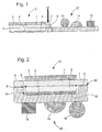
- a cell liquid crystal display (LCD) 10 connected according to the method of the invention to a printed circuit 20 (PCB) can be made of a flexible material.
- the cell usually comprises an upper glass 1 at the front of which is placed a polarizer 2, a lower lens 3, at the rear of which is placed a reflector 4, and a sealing frame 5 delimiting the liquid crystal confinement space (not visible in the figure in which the proportions in thickness have substantially been respected).
- the upper glass 1 has an extension 7 supporting on its lower surface the tracks of the electrodes.
- a printed circuit 20, supporting as electronic component for example a capa 12, a chip 14 and a quartz 16, is positioned under said extension 7, facing tracks the contact areas of the PCB to create a connection area 6 ..
- FIG. 2 relates to a second embodiment in which the PCB is positioned under the LCD.
- the LCD display cell 10 is comparable to that described in Figure 1, but the upper glass 1 has two extensions 7 and 9 which will establish two connection zones with the underlying PCB 20.
- the PCB 20 has a recess 19, which allows to accommodate the glass lower 3 and the reflector 4, so that the edges of this obviously come flush with the lower surfaces of the extensions 7, 9 supporting the tracks of the electrodes.
- the bottom of the recess 19 is lined with an adhesive 18 allowing to perform a pre-assembly, without using for example a assembly matrix. With this construction it is possible to focus the beam laser 30 in grazing incidence on the connection areas 6.8.
- the second embodiment allows to apply the method according to the invention to a display comprising several cells superimposed simply by staggering the connection areas in steps.
Landscapes
- Physics & Mathematics (AREA)
- Engineering & Computer Science (AREA)
- Nonlinear Science (AREA)
- General Physics & Mathematics (AREA)
- Mathematical Physics (AREA)
- Chemical & Material Sciences (AREA)
- Crystallography & Structural Chemistry (AREA)
- Microelectronics & Electronic Packaging (AREA)
- Manufacturing & Machinery (AREA)
- Optics & Photonics (AREA)
- Liquid Crystal (AREA)
- Devices For Indicating Variable Information By Combining Individual Elements (AREA)
- Electric Clocks (AREA)
- Wire Bonding (AREA)
- Coupling Device And Connection With Printed Circuit (AREA)
- Combinations Of Printed Boards (AREA)
Abstract
Description
- construire la cellule d'affichage en prévoyant au moins une extension de faible largeur de la glace supérieure pour supporter sur sa surface inférieure les pistes des électrodes;
- créer une zone de connexion en positionnant ladite extension sur des contacts en regard du PCB, et
- focaliser un faisceau laser sur la zone de connexion, à travers la glace supérieure ou en incidence rasante par rapport à la glace inférieure pour établir définitivement les connexions entre les pistes et les contacts du PCB. Le procédé selon l'invention ne fait donc plus intervenir aucun matériau intermédiaire et permet de réaliser l'opération de connexion dans un temps plus cours, ce qui contribue à diminuer le prix de revient du produit final.Selon un premier mode de réalisation la glace supérieure du LCD peut ne comporter qu'une seule extension et le PCB peut être connecté dans le prolongement du LCD et sensiblement dans le même plan.Selon un deuxième mode de réalisation la glace supérieure du LCD peut comporter au moins deux extensions et le PCB être situé sous le LCD. Dans ce cas le PCB présente avantageusement un évidemment permettant de loger la glace inférieure de façon à ce que les bords de l'évidemment viennent affleurer la surface inférieure de la glace supérieure. Le produit ainsi obtenu est compact et présente de bonnes propriétés mécaniques.D'autres avantages et caractéristiques de la présente invention apparaítront plus clairement à la lecture de la description ci-après faite en référence aux dessins annexés dans lesquels
- la figure 1 représente en coupe un premier mode de réalisation, et
- la figure 2 représente en coupe un deuxième mode de réalisation.
Claims (5)
- Procédé de connexion d'un circuit imprimé (PCB) aux pistes des électrodes d'une cellule d'affichage à cristaux liquides (LCD) comportant une glace supérieure, une glace inférieure et un cadre de scellement permettant de confiner lesdits cristaux liquides, caractérisé en ce qu'il consiste en les étapes suivantesconstruire la cellule d'affichage avec au moins une extension de la glace supérieure pour supporter sur sa surface inférieure les pistes des électrodes;créer une zone de connexion en positionnant ladite extension sur des contacts en regard du PCB et,focaliser un faisceau laser sur la zone de connexion à travers la glace supérieure ou en incidence rasante par rapport à la glace inférieure.
- Procédé selon la revendication 1, caractérisé en ce que la glace supérieure du LCD comporte une seule extension et que le PCB est situé sensiblement dans le même plan que le LCD.
- Procédé selon la revendication 1, caractérisé en ce que la glace supérieure du LCD comporte au moins deux extensions et que le PCB est situé sous le LCD.
- Procédé selon la revendication 3, caractérisé en ce que la glace inférieure du LCD est logée dans un évidemment pratiqué dans le PCB, les bords dudit évidemment venant affleurer la surface inférieure de la glace supérieure du LCD.
- Procédé selon l'une quelconque des revendications précédentes, caractérisé en ce que PCB est réalisé en un matériau souple.
Priority Applications (6)
| Application Number | Priority Date | Filing Date | Title |
|---|---|---|---|
| AT02076554T ATE499629T1 (de) | 2002-04-19 | 2002-04-19 | Verfahren zum verbinden einer leiterplatte mit einer flüssigkristallanzeige |
| EP02076554A EP1355187B1 (fr) | 2002-04-19 | 2002-04-19 | Procédé de connexion d'un circuit imprimé à un affichage à cristaux liquides |
| DE60239261T DE60239261D1 (de) | 2002-04-19 | 2002-04-19 | Verfahren zum Verbinden einer Leiterplatte mit einer Flüssigkristallanzeige |
| US10/403,035 US6770837B2 (en) | 2002-04-19 | 2003-04-01 | Method for connecting a printed circuit to a liquid crystal display |
| JP2003106300A JP4464065B2 (ja) | 2002-04-19 | 2003-04-10 | 液晶ディスプレイにプリント回路を接続する方法 |
| HK04102237.5A HK1059827B (en) | 2004-03-25 | Process for connection of a printed circuit board to a liquid crystal display |
Applications Claiming Priority (1)
| Application Number | Priority Date | Filing Date | Title |
|---|---|---|---|
| EP02076554A EP1355187B1 (fr) | 2002-04-19 | 2002-04-19 | Procédé de connexion d'un circuit imprimé à un affichage à cristaux liquides |
Publications (2)
| Publication Number | Publication Date |
|---|---|
| EP1355187A1 true EP1355187A1 (fr) | 2003-10-22 |
| EP1355187B1 EP1355187B1 (fr) | 2011-02-23 |
Family
ID=28459557
Family Applications (1)
| Application Number | Title | Priority Date | Filing Date |
|---|---|---|---|
| EP02076554A Expired - Lifetime EP1355187B1 (fr) | 2002-04-19 | 2002-04-19 | Procédé de connexion d'un circuit imprimé à un affichage à cristaux liquides |
Country Status (5)
| Country | Link |
|---|---|
| US (1) | US6770837B2 (fr) |
| EP (1) | EP1355187B1 (fr) |
| JP (1) | JP4464065B2 (fr) |
| AT (1) | ATE499629T1 (fr) |
| DE (1) | DE60239261D1 (fr) |
Families Citing this family (1)
| Publication number | Priority date | Publication date | Assignee | Title |
|---|---|---|---|---|
| FI123860B (fi) | 2010-05-18 | 2013-11-29 | Corelase Oy | Menetelmä substraattien tiivistämiseksi ja kontaktoimiseksi laservalon avulla ja elektroniikkamoduli |
Citations (4)
| Publication number | Priority date | Publication date | Assignee | Title |
|---|---|---|---|---|
| US4654965A (en) * | 1984-07-16 | 1987-04-07 | Ricoh Company, Ltd. | Method of manufacturing liquid crystal display unit |
| JPS63241523A (ja) * | 1987-03-30 | 1988-10-06 | Toshiba Corp | 液晶パネル基板装置 |
| US4836651A (en) * | 1987-12-03 | 1989-06-06 | Anderson Richard A | Flexible circuit interconnection for a matrix addressed liquid crystal panel |
| US5606440A (en) * | 1992-04-30 | 1997-02-25 | Sharp Kabushiki Kaisha | Assembling method of flat type display device |
Family Cites Families (6)
| Publication number | Priority date | Publication date | Assignee | Title |
|---|---|---|---|---|
| JPH0820638B2 (ja) * | 1986-08-08 | 1996-03-04 | 株式会社半導体エネルギ−研究所 | 液晶装置およびその作製方法 |
| US5102361A (en) * | 1989-01-23 | 1992-04-07 | Sharp Kabushiki Kaisha | Method for the manufacture of active matrix display apparatuses |
| TW305948B (fr) * | 1993-11-08 | 1997-05-21 | Hitachi Ltd | |
| JP4498489B2 (ja) * | 1999-03-19 | 2010-07-07 | シャープ株式会社 | 液晶表示装置とその製造方法 |
| JP4001712B2 (ja) * | 2000-03-29 | 2007-10-31 | シャープ株式会社 | 液晶表示装置の欠陥修復方法 |
| JP2002196352A (ja) * | 2000-12-07 | 2002-07-12 | Koninkl Philips Electronics Nv | 予備配線を有する液晶表示装置 |
-
2002
- 2002-04-19 AT AT02076554T patent/ATE499629T1/de not_active IP Right Cessation
- 2002-04-19 DE DE60239261T patent/DE60239261D1/de not_active Expired - Lifetime
- 2002-04-19 EP EP02076554A patent/EP1355187B1/fr not_active Expired - Lifetime
-
2003
- 2003-04-01 US US10/403,035 patent/US6770837B2/en not_active Expired - Lifetime
- 2003-04-10 JP JP2003106300A patent/JP4464065B2/ja not_active Expired - Fee Related
Patent Citations (4)
| Publication number | Priority date | Publication date | Assignee | Title |
|---|---|---|---|---|
| US4654965A (en) * | 1984-07-16 | 1987-04-07 | Ricoh Company, Ltd. | Method of manufacturing liquid crystal display unit |
| JPS63241523A (ja) * | 1987-03-30 | 1988-10-06 | Toshiba Corp | 液晶パネル基板装置 |
| US4836651A (en) * | 1987-12-03 | 1989-06-06 | Anderson Richard A | Flexible circuit interconnection for a matrix addressed liquid crystal panel |
| US5606440A (en) * | 1992-04-30 | 1997-02-25 | Sharp Kabushiki Kaisha | Assembling method of flat type display device |
Non-Patent Citations (2)
| Title |
|---|
| "COMPACT LIQUID CRYSTAL DISPLAY MODULE STRUCTURE", IBM TECHNICAL DISCLOSURE BULLETIN, IBM CORP. NEW YORK, US, vol. 40, no. 2, 1 February 1997 (1997-02-01), pages 227 - 228, XP000692230, ISSN: 0018-8689 * |
| PATENT ABSTRACTS OF JAPAN vol. 013, no. 047 (P - 822) 3 February 1989 (1989-02-03) * |
Also Published As
| Publication number | Publication date |
|---|---|
| ATE499629T1 (de) | 2011-03-15 |
| US6770837B2 (en) | 2004-08-03 |
| HK1059827A1 (en) | 2004-07-16 |
| US20030197827A1 (en) | 2003-10-23 |
| JP4464065B2 (ja) | 2010-05-19 |
| DE60239261D1 (de) | 2011-04-07 |
| JP2003315823A (ja) | 2003-11-06 |
| EP1355187B1 (fr) | 2011-02-23 |
Similar Documents
| Publication | Publication Date | Title |
|---|---|---|
| FR2594992A1 (fr) | Dispositif d'affichage a cristal liquide | |
| EP3650958B1 (fr) | Objet muni d'un dispositif d'affichage electrooptique | |
| FR2482344A1 (fr) | Afficheur bidimensionnel a couche fluide commandee electriquement et son procede de fabrication | |
| EP1780616A3 (fr) | Ensemble d'affichage à effets décoratifs pour un instrument portable, tel qu'une montre | |
| EP0324700A1 (fr) | Boîtier destiné à contenir un élément fragile tel qu'un circuit logique et procédé d'assemblage d'un tel boîtier | |
| EP2477084A1 (fr) | Montre comprenant un connecteur zébra pour la connexion électrique entre un dispositif d'affichage numérique et une carte de circuit imprimé et procédé d'assemblage d'une telle montre | |
| EP1734423B1 (fr) | Assemblage d'une glace tactile sur un boîtier | |
| EP1355187B1 (fr) | Procédé de connexion d'un circuit imprimé à un affichage à cristaux liquides | |
| FR2762115A1 (fr) | Procede d'insertion d'un module electronique dans un corps de carte a memoire electronique | |
| EP2584413B1 (fr) | Procédé de fixation d'une glace sur une carrure d'une boîte de montre | |
| FR2987169A1 (fr) | Procede de liaison d'un premier composant electronique a un deuxieme composant | |
| FR2844606A1 (fr) | Miroir electrochrome, et couche reflechissante pour ledit miroir | |
| EP0828413B1 (fr) | Dispositif d'affichage électro-optique et support flexible pour de tels dispositifs servant à l'alimentation de ces dispositifs | |
| EP2673676B1 (fr) | Montre comprenant une lunette et procede de fixation d'une telle lunette | |
| EP1055149B1 (fr) | Cellule electro-optique ou cellule photovoltaique electrochimique, et procede de fabrication d'une telle cellule | |
| EP1734422A1 (fr) | Assemblage d'une glace tactile sur un boîtier | |
| EP2732318B1 (fr) | Guide de lumière pour l'éclairage d'un dispositif d'affichage d'informations | |
| EP2447790A1 (fr) | Glace servant à fermer par le haut la boîte d'un objet portable | |
| FR2637110A1 (fr) | Cellule electro-optique perfectionnee | |
| CH704453A2 (fr) | Montre comprenant une lunette et procédé de fixation d'une telle lunette. | |
| CH703966A2 (fr) | Glace servant à fermer par le haut la boîte d'un objet portable. | |
| CH722082A1 (fr) | Dispositif horloger assurant une étanchéité à grande profondeur | |
| CH703289B1 (fr) | Dispositif d'encapsulage pour MEMS. | |
| FR2817398A1 (fr) | Boitier en film ultra-mince | |
| CH705659A2 (fr) | Procédé de fixation d'une glace sur une carrure d'une boîte de montre. |
Legal Events
| Date | Code | Title | Description |
|---|---|---|---|
| PUAI | Public reference made under article 153(3) epc to a published international application that has entered the european phase |
Free format text: ORIGINAL CODE: 0009012 |
|
| AK | Designated contracting states |
Kind code of ref document: A1 Designated state(s): AT BE CH CY DE DK ES FI FR GB GR IE IT LI LU MC NL PT SE TR |
|
| AX | Request for extension of the european patent |
Extension state: AL LT LV MK RO SI |
|
| 17P | Request for examination filed |
Effective date: 20040422 |
|
| 17Q | First examination report despatched |
Effective date: 20040524 |
|
| AKX | Designation fees paid |
Designated state(s): AT BE CH CY DE DK ES FI FR GB GR IE IT LI LU MC NL PT SE TR |
|
| REG | Reference to a national code |
Ref country code: HK Ref legal event code: DE Ref document number: 1059827 Country of ref document: HK |
|
| GRAP | Despatch of communication of intention to grant a patent |
Free format text: ORIGINAL CODE: EPIDOSNIGR1 |
|
| GRAS | Grant fee paid |
Free format text: ORIGINAL CODE: EPIDOSNIGR3 |
|
| GRAA | (expected) grant |
Free format text: ORIGINAL CODE: 0009210 |
|
| AK | Designated contracting states |
Kind code of ref document: B1 Designated state(s): AT BE CH CY DE DK ES FI FR GB GR IE IT LI LU MC NL PT SE TR |
|
| REG | Reference to a national code |
Ref country code: GB Ref legal event code: FG4D Free format text: NOT ENGLISH |
|
| REG | Reference to a national code |
Ref country code: CH Ref legal event code: EP Ref country code: CH Ref legal event code: NV Representative=s name: ICB INGENIEURS CONSEILS EN BREVETS SA |
|
| REG | Reference to a national code |
Ref country code: IE Ref legal event code: FG4D Free format text: LANGUAGE OF EP DOCUMENT: FRENCH |
|
| REF | Corresponds to: |
Ref document number: 60239261 Country of ref document: DE Date of ref document: 20110407 Kind code of ref document: P |
|
| REG | Reference to a national code |
Ref country code: DE Ref legal event code: R096 Ref document number: 60239261 Country of ref document: DE Effective date: 20110407 |
|
| REG | Reference to a national code |
Ref country code: HK Ref legal event code: GR Ref document number: 1059827 Country of ref document: HK |
|
| REG | Reference to a national code |
Ref country code: NL Ref legal event code: VDEP Effective date: 20110223 |
|
| PG25 | Lapsed in a contracting state [announced via postgrant information from national office to epo] |
Ref country code: GR Free format text: LAPSE BECAUSE OF FAILURE TO SUBMIT A TRANSLATION OF THE DESCRIPTION OR TO PAY THE FEE WITHIN THE PRESCRIBED TIME-LIMIT Effective date: 20110524 Ref country code: SE Free format text: LAPSE BECAUSE OF FAILURE TO SUBMIT A TRANSLATION OF THE DESCRIPTION OR TO PAY THE FEE WITHIN THE PRESCRIBED TIME-LIMIT Effective date: 20110223 Ref country code: PT Free format text: LAPSE BECAUSE OF FAILURE TO SUBMIT A TRANSLATION OF THE DESCRIPTION OR TO PAY THE FEE WITHIN THE PRESCRIBED TIME-LIMIT Effective date: 20110623 Ref country code: ES Free format text: LAPSE BECAUSE OF FAILURE TO SUBMIT A TRANSLATION OF THE DESCRIPTION OR TO PAY THE FEE WITHIN THE PRESCRIBED TIME-LIMIT Effective date: 20110603 |
|
| PG25 | Lapsed in a contracting state [announced via postgrant information from national office to epo] |
Ref country code: NL Free format text: LAPSE BECAUSE OF FAILURE TO SUBMIT A TRANSLATION OF THE DESCRIPTION OR TO PAY THE FEE WITHIN THE PRESCRIBED TIME-LIMIT Effective date: 20110223 Ref country code: CY Free format text: LAPSE BECAUSE OF FAILURE TO SUBMIT A TRANSLATION OF THE DESCRIPTION OR TO PAY THE FEE WITHIN THE PRESCRIBED TIME-LIMIT Effective date: 20110223 Ref country code: AT Free format text: LAPSE BECAUSE OF FAILURE TO SUBMIT A TRANSLATION OF THE DESCRIPTION OR TO PAY THE FEE WITHIN THE PRESCRIBED TIME-LIMIT Effective date: 20110223 Ref country code: FI Free format text: LAPSE BECAUSE OF FAILURE TO SUBMIT A TRANSLATION OF THE DESCRIPTION OR TO PAY THE FEE WITHIN THE PRESCRIBED TIME-LIMIT Effective date: 20110223 |
|
| REG | Reference to a national code |
Ref country code: IE Ref legal event code: FD4D |
|
| BERE | Be: lapsed |
Owner name: ETA SA MANUFACTURE HORLOGERE SUISSE Effective date: 20110430 |
|
| PG25 | Lapsed in a contracting state [announced via postgrant information from national office to epo] |
Ref country code: DK Free format text: LAPSE BECAUSE OF FAILURE TO SUBMIT A TRANSLATION OF THE DESCRIPTION OR TO PAY THE FEE WITHIN THE PRESCRIBED TIME-LIMIT Effective date: 20110223 Ref country code: IE Free format text: LAPSE BECAUSE OF FAILURE TO SUBMIT A TRANSLATION OF THE DESCRIPTION OR TO PAY THE FEE WITHIN THE PRESCRIBED TIME-LIMIT Effective date: 20110223 |
|
| PG25 | Lapsed in a contracting state [announced via postgrant information from national office to epo] |
Ref country code: MC Free format text: LAPSE BECAUSE OF NON-PAYMENT OF DUE FEES Effective date: 20110430 |
|
| PLBE | No opposition filed within time limit |
Free format text: ORIGINAL CODE: 0009261 |
|
| STAA | Information on the status of an ep patent application or granted ep patent |
Free format text: STATUS: NO OPPOSITION FILED WITHIN TIME LIMIT |
|
| GBPC | Gb: european patent ceased through non-payment of renewal fee |
Effective date: 20110523 |
|
| PG25 | Lapsed in a contracting state [announced via postgrant information from national office to epo] |
Ref country code: BE Free format text: LAPSE BECAUSE OF NON-PAYMENT OF DUE FEES Effective date: 20110430 |
|
| 26N | No opposition filed |
Effective date: 20111124 |
|
| REG | Reference to a national code |
Ref country code: DE Ref legal event code: R097 Ref document number: 60239261 Country of ref document: DE Effective date: 20111124 |
|
| PG25 | Lapsed in a contracting state [announced via postgrant information from national office to epo] |
Ref country code: IT Free format text: LAPSE BECAUSE OF FAILURE TO SUBMIT A TRANSLATION OF THE DESCRIPTION OR TO PAY THE FEE WITHIN THE PRESCRIBED TIME-LIMIT Effective date: 20110223 |
|
| PG25 | Lapsed in a contracting state [announced via postgrant information from national office to epo] |
Ref country code: GB Free format text: LAPSE BECAUSE OF NON-PAYMENT OF DUE FEES Effective date: 20110523 |
|
| PG25 | Lapsed in a contracting state [announced via postgrant information from national office to epo] |
Ref country code: LU Free format text: LAPSE BECAUSE OF NON-PAYMENT OF DUE FEES Effective date: 20110419 |
|
| PGFP | Annual fee paid to national office [announced via postgrant information from national office to epo] |
Ref country code: DE Payment date: 20130322 Year of fee payment: 12 |
|
| PGFP | Annual fee paid to national office [announced via postgrant information from national office to epo] |
Ref country code: FR Payment date: 20130603 Year of fee payment: 12 |
|
| PG25 | Lapsed in a contracting state [announced via postgrant information from national office to epo] |
Ref country code: TR Free format text: LAPSE BECAUSE OF FAILURE TO SUBMIT A TRANSLATION OF THE DESCRIPTION OR TO PAY THE FEE WITHIN THE PRESCRIBED TIME-LIMIT Effective date: 20110223 |
|
| REG | Reference to a national code |
Ref country code: DE Ref legal event code: R119 Ref document number: 60239261 Country of ref document: DE |
|
| REG | Reference to a national code |
Ref country code: FR Ref legal event code: ST Effective date: 20141231 |
|
| PG25 | Lapsed in a contracting state [announced via postgrant information from national office to epo] |
Ref country code: DE Free format text: LAPSE BECAUSE OF NON-PAYMENT OF DUE FEES Effective date: 20141101 |
|
| REG | Reference to a national code |
Ref country code: DE Ref legal event code: R119 Ref document number: 60239261 Country of ref document: DE Effective date: 20141101 |
|
| PG25 | Lapsed in a contracting state [announced via postgrant information from national office to epo] |
Ref country code: FR Free format text: LAPSE BECAUSE OF NON-PAYMENT OF DUE FEES Effective date: 20140430 |
|
| PGFP | Annual fee paid to national office [announced via postgrant information from national office to epo] |
Ref country code: CH Payment date: 20210326 Year of fee payment: 20 |
|
| REG | Reference to a national code |
Ref country code: CH Ref legal event code: PL |