EP1355199A2 - Elément conducteur, unité de traitement et appareil électrophotographique l'utilisant - Google Patents
Elément conducteur, unité de traitement et appareil électrophotographique l'utilisant Download PDFInfo
- Publication number
- EP1355199A2 EP1355199A2 EP03008919A EP03008919A EP1355199A2 EP 1355199 A2 EP1355199 A2 EP 1355199A2 EP 03008919 A EP03008919 A EP 03008919A EP 03008919 A EP03008919 A EP 03008919A EP 1355199 A2 EP1355199 A2 EP 1355199A2
- Authority
- EP
- European Patent Office
- Prior art keywords
- surface layer
- fine particles
- conductive member
- layer
- average particle
- Prior art date
- Legal status (The legal status is an assumption and is not a legal conclusion. Google has not performed a legal analysis and makes no representation as to the accuracy of the status listed.)
- Granted
Links
- 238000000034 method Methods 0.000 title claims abstract description 51
- 230000008569 process Effects 0.000 title claims abstract description 31
- 239000002344 surface layer Substances 0.000 claims abstract description 226
- 239000010410 layer Substances 0.000 claims abstract description 195
- 239000010419 fine particle Substances 0.000 claims abstract description 166
- 239000002245 particle Substances 0.000 claims abstract description 121
- 239000000463 material Substances 0.000 claims description 72
- 238000012546 transfer Methods 0.000 claims description 33
- 239000006229 carbon black Substances 0.000 claims description 18
- 239000011230 binding agent Substances 0.000 claims description 16
- 125000004433 nitrogen atom Chemical group N* 0.000 claims description 3
- 229910052757 nitrogen Inorganic materials 0.000 claims 1
- 125000004430 oxygen atom Chemical group O* 0.000 claims 1
- 238000000576 coating method Methods 0.000 description 141
- 239000011248 coating agent Substances 0.000 description 135
- 239000012530 fluid Substances 0.000 description 111
- 238000007598 dipping method Methods 0.000 description 107
- 239000006185 dispersion Substances 0.000 description 36
- 230000000052 comparative effect Effects 0.000 description 27
- 239000000047 product Substances 0.000 description 26
- 229920005989 resin Polymers 0.000 description 22
- 239000011347 resin Substances 0.000 description 22
- 238000011156 evaluation Methods 0.000 description 21
- 239000007788 liquid Substances 0.000 description 18
- 239000011324 bead Substances 0.000 description 16
- 239000000203 mixture Substances 0.000 description 16
- 150000001875 compounds Chemical class 0.000 description 14
- 239000002612 dispersion medium Substances 0.000 description 14
- 239000011521 glass Substances 0.000 description 13
- 229920002725 thermoplastic elastomer Polymers 0.000 description 13
- OKKJLVBELUTLKV-UHFFFAOYSA-N Methanol Chemical compound OC OKKJLVBELUTLKV-UHFFFAOYSA-N 0.000 description 12
- YXFVVABEGXRONW-UHFFFAOYSA-N Toluene Chemical compound CC1=CC=CC=C1 YXFVVABEGXRONW-UHFFFAOYSA-N 0.000 description 12
- XLOMVQKBTHCTTD-UHFFFAOYSA-N Zinc monoxide Chemical compound [Zn]=O XLOMVQKBTHCTTD-UHFFFAOYSA-N 0.000 description 12
- OKTJSMMVPCPJKN-UHFFFAOYSA-N Carbon Chemical compound [C] OKTJSMMVPCPJKN-UHFFFAOYSA-N 0.000 description 11
- 239000003973 paint Substances 0.000 description 11
- 238000012856 packing Methods 0.000 description 10
- XOLBLPGZBRYERU-UHFFFAOYSA-N tin dioxide Chemical compound O=[Sn]=O XOLBLPGZBRYERU-UHFFFAOYSA-N 0.000 description 10
- 229910001887 tin oxide Inorganic materials 0.000 description 10
- ZWEHNKRNPOVVGH-UHFFFAOYSA-N 2-Butanone Chemical compound CCC(C)=O ZWEHNKRNPOVVGH-UHFFFAOYSA-N 0.000 description 9
- GWEVSGVZZGPLCZ-UHFFFAOYSA-N Titan oxide Chemical compound O=[Ti]=O GWEVSGVZZGPLCZ-UHFFFAOYSA-N 0.000 description 9
- 238000010276 construction Methods 0.000 description 9
- 229920001971 elastomer Polymers 0.000 description 9
- 238000004381 surface treatment Methods 0.000 description 9
- LFQSCWFLJHTTHZ-UHFFFAOYSA-N Ethanol Chemical compound CCO LFQSCWFLJHTTHZ-UHFFFAOYSA-N 0.000 description 8
- 230000000694 effects Effects 0.000 description 8
- 150000004706 metal oxides Chemical class 0.000 description 8
- 229920005996 polystyrene-poly(ethylene-butylene)-polystyrene Polymers 0.000 description 8
- 238000007605 air drying Methods 0.000 description 7
- 230000015572 biosynthetic process Effects 0.000 description 7
- 239000005356 container glass Substances 0.000 description 7
- CZWLNMOIEMTDJY-UHFFFAOYSA-N hexyl(trimethoxy)silane Chemical compound CCCCCC[Si](OC)(OC)OC CZWLNMOIEMTDJY-UHFFFAOYSA-N 0.000 description 7
- 229910044991 metal oxide Inorganic materials 0.000 description 7
- VTYYLEPIZMXCLO-UHFFFAOYSA-L Calcium carbonate Chemical compound [Ca+2].[O-]C([O-])=O VTYYLEPIZMXCLO-UHFFFAOYSA-L 0.000 description 6
- 239000003795 chemical substances by application Substances 0.000 description 6
- 238000001035 drying Methods 0.000 description 6
- 239000013013 elastic material Substances 0.000 description 6
- 239000002994 raw material Substances 0.000 description 6
- 239000011787 zinc oxide Substances 0.000 description 6
- VYPSYNLAJGMNEJ-UHFFFAOYSA-N Silicium dioxide Chemical compound O=[Si]=O VYPSYNLAJGMNEJ-UHFFFAOYSA-N 0.000 description 5
- 230000005540 biological transmission Effects 0.000 description 5
- 239000002019 doping agent Substances 0.000 description 5
- 239000000806 elastomer Substances 0.000 description 5
- 229910052751 metal Inorganic materials 0.000 description 5
- 239000002184 metal Substances 0.000 description 5
- 239000003921 oil Substances 0.000 description 5
- 229920002037 poly(vinyl butyral) polymer Polymers 0.000 description 5
- 239000002356 single layer Substances 0.000 description 5
- 239000000243 solution Substances 0.000 description 5
- OGIDPMRJRNCKJF-UHFFFAOYSA-N titanium oxide Inorganic materials [Ti]=O OGIDPMRJRNCKJF-UHFFFAOYSA-N 0.000 description 5
- 239000005057 Hexamethylene diisocyanate Substances 0.000 description 4
- PXHVJJICTQNCMI-UHFFFAOYSA-N Nickel Chemical compound [Ni] PXHVJJICTQNCMI-UHFFFAOYSA-N 0.000 description 4
- 229920000459 Nitrile rubber Polymers 0.000 description 4
- 230000007547 defect Effects 0.000 description 4
- FFUAGWLWBBFQJT-UHFFFAOYSA-N hexamethyldisilazane Chemical compound C[Si](C)(C)N[Si](C)(C)C FFUAGWLWBBFQJT-UHFFFAOYSA-N 0.000 description 4
- RRAMGCGOFNQTLD-UHFFFAOYSA-N hexamethylene diisocyanate Chemical compound O=C=NCCCCCCN=C=O RRAMGCGOFNQTLD-UHFFFAOYSA-N 0.000 description 4
- 238000005259 measurement Methods 0.000 description 4
- 230000002093 peripheral effect Effects 0.000 description 4
- 239000005060 rubber Substances 0.000 description 4
- 239000007787 solid Substances 0.000 description 4
- 229910001220 stainless steel Inorganic materials 0.000 description 4
- 239000010935 stainless steel Substances 0.000 description 4
- 229920003051 synthetic elastomer Polymers 0.000 description 4
- 239000005061 synthetic rubber Substances 0.000 description 4
- WHIVNJATOVLWBW-PLNGDYQASA-N (nz)-n-butan-2-ylidenehydroxylamine Chemical compound CC\C(C)=N/O WHIVNJATOVLWBW-PLNGDYQASA-N 0.000 description 3
- YXIWHUQXZSMYRE-UHFFFAOYSA-N 1,3-benzothiazole-2-thiol Chemical compound C1=CC=C2SC(S)=NC2=C1 YXIWHUQXZSMYRE-UHFFFAOYSA-N 0.000 description 3
- YHMYGUUIMTVXNW-UHFFFAOYSA-N 1,3-dihydrobenzimidazole-2-thione Chemical compound C1=CC=C2NC(S)=NC2=C1 YHMYGUUIMTVXNW-UHFFFAOYSA-N 0.000 description 3
- IEKHISJGRIEHRE-UHFFFAOYSA-N 16-methylheptadecanoic acid;propan-2-ol;titanium Chemical compound [Ti].CC(C)O.CC(C)CCCCCCCCCCCCCCC(O)=O.CC(C)CCCCCCCCCCCCCCC(O)=O.CC(C)CCCCCCCCCCCCCCC(O)=O IEKHISJGRIEHRE-UHFFFAOYSA-N 0.000 description 3
- YCKRFDGAMUMZLT-UHFFFAOYSA-N Fluorine atom Chemical compound [F] YCKRFDGAMUMZLT-UHFFFAOYSA-N 0.000 description 3
- 239000005062 Polybutadiene Substances 0.000 description 3
- 235000021355 Stearic acid Nutrition 0.000 description 3
- NINIDFKCEFEMDL-UHFFFAOYSA-N Sulfur Chemical compound [S] NINIDFKCEFEMDL-UHFFFAOYSA-N 0.000 description 3
- 239000002253 acid Substances 0.000 description 3
- 230000006978 adaptation Effects 0.000 description 3
- 229910052782 aluminium Inorganic materials 0.000 description 3
- XAGFODPZIPBFFR-UHFFFAOYSA-N aluminium Chemical compound [Al] XAGFODPZIPBFFR-UHFFFAOYSA-N 0.000 description 3
- 229910000019 calcium carbonate Inorganic materials 0.000 description 3
- 125000004432 carbon atom Chemical group C* 0.000 description 3
- 230000008859 change Effects 0.000 description 3
- 238000011161 development Methods 0.000 description 3
- 235000014113 dietary fatty acids Nutrition 0.000 description 3
- 238000009826 distribution Methods 0.000 description 3
- 239000000194 fatty acid Substances 0.000 description 3
- 229930195729 fatty acid Natural products 0.000 description 3
- 150000004665 fatty acids Chemical class 0.000 description 3
- 239000011737 fluorine Substances 0.000 description 3
- 229910052731 fluorine Inorganic materials 0.000 description 3
- 238000010438 heat treatment Methods 0.000 description 3
- 230000006872 improvement Effects 0.000 description 3
- 239000000314 lubricant Substances 0.000 description 3
- 238000002156 mixing Methods 0.000 description 3
- QIQXTHQIDYTFRH-UHFFFAOYSA-N octadecanoic acid Chemical compound CCCCCCCCCCCCCCCCCC(O)=O QIQXTHQIDYTFRH-UHFFFAOYSA-N 0.000 description 3
- OQCDKBAXFALNLD-UHFFFAOYSA-N octadecanoic acid Natural products CCCCCCCC(C)CCCCCCCCC(O)=O OQCDKBAXFALNLD-UHFFFAOYSA-N 0.000 description 3
- 239000004014 plasticizer Substances 0.000 description 3
- 229920002857 polybutadiene Polymers 0.000 description 3
- 229920000642 polymer Polymers 0.000 description 3
- 229920005862 polyol Polymers 0.000 description 3
- 229920005749 polyurethane resin Polymers 0.000 description 3
- 238000012545 processing Methods 0.000 description 3
- 230000003014 reinforcing effect Effects 0.000 description 3
- 239000008117 stearic acid Substances 0.000 description 3
- 229910052717 sulfur Inorganic materials 0.000 description 3
- 239000011593 sulfur Substances 0.000 description 3
- 238000004073 vulcanization Methods 0.000 description 3
- 229920000178 Acrylic resin Polymers 0.000 description 2
- 239000004925 Acrylic resin Substances 0.000 description 2
- RYGMFSIKBFXOCR-UHFFFAOYSA-N Copper Chemical compound [Cu] RYGMFSIKBFXOCR-UHFFFAOYSA-N 0.000 description 2
- 229920000089 Cyclic olefin copolymer Polymers 0.000 description 2
- JOYRKODLDBILNP-UHFFFAOYSA-N Ethyl urethane Chemical compound CCOC(N)=O JOYRKODLDBILNP-UHFFFAOYSA-N 0.000 description 2
- XEEYBQQBJWHFJM-UHFFFAOYSA-N Iron Chemical compound [Fe] XEEYBQQBJWHFJM-UHFFFAOYSA-N 0.000 description 2
- UQSXHKLRYXJYBZ-UHFFFAOYSA-N Iron oxide Chemical compound [Fe]=O UQSXHKLRYXJYBZ-UHFFFAOYSA-N 0.000 description 2
- NTIZESTWPVYFNL-UHFFFAOYSA-N Methyl isobutyl ketone Chemical compound CC(C)CC(C)=O NTIZESTWPVYFNL-UHFFFAOYSA-N 0.000 description 2
- UIHCLUNTQKBZGK-UHFFFAOYSA-N Methyl isobutyl ketone Natural products CCC(C)C(C)=O UIHCLUNTQKBZGK-UHFFFAOYSA-N 0.000 description 2
- PPBRXRYQALVLMV-UHFFFAOYSA-N Styrene Chemical compound C=CC1=CC=CC=C1 PPBRXRYQALVLMV-UHFFFAOYSA-N 0.000 description 2
- 238000010306 acid treatment Methods 0.000 description 2
- 125000001931 aliphatic group Chemical group 0.000 description 2
- PNEYBMLMFCGWSK-UHFFFAOYSA-N aluminium oxide Inorganic materials [O-2].[O-2].[O-2].[Al+3].[Al+3] PNEYBMLMFCGWSK-UHFFFAOYSA-N 0.000 description 2
- ADCOVFLJGNWWNZ-UHFFFAOYSA-N antimony trioxide Chemical compound O=[Sb]O[Sb]=O ADCOVFLJGNWWNZ-UHFFFAOYSA-N 0.000 description 2
- TZCXTZWJZNENPQ-UHFFFAOYSA-L barium sulfate Chemical compound [Ba+2].[O-]S([O-])(=O)=O TZCXTZWJZNENPQ-UHFFFAOYSA-L 0.000 description 2
- QHIWVLPBUQWDMQ-UHFFFAOYSA-N butyl prop-2-enoate;methyl 2-methylprop-2-enoate;prop-2-enoic acid Chemical compound OC(=O)C=C.COC(=O)C(C)=C.CCCCOC(=O)C=C QHIWVLPBUQWDMQ-UHFFFAOYSA-N 0.000 description 2
- 229910052799 carbon Inorganic materials 0.000 description 2
- 229920001577 copolymer Polymers 0.000 description 2
- 229910052802 copper Inorganic materials 0.000 description 2
- 239000010949 copper Substances 0.000 description 2
- 230000008878 coupling Effects 0.000 description 2
- 238000010168 coupling process Methods 0.000 description 2
- 238000005859 coupling reaction Methods 0.000 description 2
- 229920005558 epichlorohydrin rubber Polymers 0.000 description 2
- 239000006260 foam Substances 0.000 description 2
- 238000010097 foam moulding Methods 0.000 description 2
- 239000010439 graphite Substances 0.000 description 2
- 229910002804 graphite Inorganic materials 0.000 description 2
- 230000002209 hydrophobic effect Effects 0.000 description 2
- 229910003437 indium oxide Inorganic materials 0.000 description 2
- PJXISJQVUVHSOJ-UHFFFAOYSA-N indium(iii) oxide Chemical compound [O-2].[O-2].[O-2].[In+3].[In+3] PJXISJQVUVHSOJ-UHFFFAOYSA-N 0.000 description 2
- 230000001788 irregular Effects 0.000 description 2
- 229920003049 isoprene rubber Polymers 0.000 description 2
- 230000007246 mechanism Effects 0.000 description 2
- VNWKTOKETHGBQD-UHFFFAOYSA-N methane Chemical compound C VNWKTOKETHGBQD-UHFFFAOYSA-N 0.000 description 2
- KELHQGOVULCJSG-UHFFFAOYSA-N n,n-dimethyl-1-(5-methylfuran-2-yl)ethane-1,2-diamine Chemical compound CN(C)C(CN)C1=CC=C(C)O1 KELHQGOVULCJSG-UHFFFAOYSA-N 0.000 description 2
- 229910052759 nickel Inorganic materials 0.000 description 2
- 230000003287 optical effect Effects 0.000 description 2
- 230000036961 partial effect Effects 0.000 description 2
- 229920001084 poly(chloroprene) Polymers 0.000 description 2
- 229920006122 polyamide resin Polymers 0.000 description 2
- 238000007639 printing Methods 0.000 description 2
- 150000003242 quaternary ammonium salts Chemical class 0.000 description 2
- 229920002050 silicone resin Polymers 0.000 description 2
- 229920003048 styrene butadiene rubber Polymers 0.000 description 2
- 239000000126 substance Substances 0.000 description 2
- 238000012360 testing method Methods 0.000 description 2
- 239000004408 titanium dioxide Substances 0.000 description 2
- JLGNHOJUQFHYEZ-UHFFFAOYSA-N trimethoxy(3,3,3-trifluoropropyl)silane Chemical compound CO[Si](OC)(OC)CCC(F)(F)F JLGNHOJUQFHYEZ-UHFFFAOYSA-N 0.000 description 2
- STMDPCBYJCIZOD-UHFFFAOYSA-N 2-(2,4-dinitroanilino)-4-methylpentanoic acid Chemical compound CC(C)CC(C(O)=O)NC1=CC=C([N+]([O-])=O)C=C1[N+]([O-])=O STMDPCBYJCIZOD-UHFFFAOYSA-N 0.000 description 1
- DFWCPLGXFMSUCW-UHFFFAOYSA-N 3-(dimethylamino)propyl carbamimidothioate;hydron;dichloride Chemical compound Cl.Cl.CN(C)CCCSC(N)=N DFWCPLGXFMSUCW-UHFFFAOYSA-N 0.000 description 1
- BUZICZZQJDLXJN-UHFFFAOYSA-N 3-azaniumyl-4-hydroxybutanoate Chemical compound OCC(N)CC(O)=O BUZICZZQJDLXJN-UHFFFAOYSA-N 0.000 description 1
- 229920002799 BoPET Polymers 0.000 description 1
- CKXFVRQVHVLLGH-UHFFFAOYSA-N CC(CC)=NO.C(CCCCCN=C=O)N=C=O Chemical compound CC(CC)=NO.C(CCCCCN=C=O)N=C=O CKXFVRQVHVLLGH-UHFFFAOYSA-N 0.000 description 1
- DFBJNRYLLHMZFZ-UHFFFAOYSA-N CC(CC)=NO.O=C=NC1CC(CN=C=O)(CC(C1)(C)C)C Chemical compound CC(CC)=NO.O=C=NC1CC(CN=C=O)(CC(C1)(C)C)C DFBJNRYLLHMZFZ-UHFFFAOYSA-N 0.000 description 1
- 229920000049 Carbon (fiber) Polymers 0.000 description 1
- 239000004709 Chlorinated polyethylene Substances 0.000 description 1
- BRLQWZUYTZBJKN-UHFFFAOYSA-N Epichlorohydrin Chemical compound ClCC1CO1 BRLQWZUYTZBJKN-UHFFFAOYSA-N 0.000 description 1
- 239000005977 Ethylene Substances 0.000 description 1
- IAYPIBMASNFSPL-UHFFFAOYSA-N Ethylene oxide Chemical compound C1CO1 IAYPIBMASNFSPL-UHFFFAOYSA-N 0.000 description 1
- 229910001111 Fine metal Inorganic materials 0.000 description 1
- 244000043261 Hevea brasiliensis Species 0.000 description 1
- 239000005909 Kieselgur Substances 0.000 description 1
- 240000007594 Oryza sativa Species 0.000 description 1
- 235000007164 Oryza sativa Nutrition 0.000 description 1
- 239000005662 Paraffin oil Substances 0.000 description 1
- 239000004952 Polyamide Substances 0.000 description 1
- 239000004793 Polystyrene Substances 0.000 description 1
- 239000006087 Silane Coupling Agent Substances 0.000 description 1
- XUIMIQQOPSSXEZ-UHFFFAOYSA-N Silicon Chemical group [Si] XUIMIQQOPSSXEZ-UHFFFAOYSA-N 0.000 description 1
- BQCADISMDOOEFD-UHFFFAOYSA-N Silver Chemical compound [Ag] BQCADISMDOOEFD-UHFFFAOYSA-N 0.000 description 1
- 239000002174 Styrene-butadiene Substances 0.000 description 1
- UCKMPCXJQFINFW-UHFFFAOYSA-N Sulphide Chemical compound [S-2] UCKMPCXJQFINFW-UHFFFAOYSA-N 0.000 description 1
- ATJFFYVFTNAWJD-UHFFFAOYSA-N Tin Chemical compound [Sn] ATJFFYVFTNAWJD-UHFFFAOYSA-N 0.000 description 1
- RTAQQCXQSZGOHL-UHFFFAOYSA-N Titanium Chemical compound [Ti] RTAQQCXQSZGOHL-UHFFFAOYSA-N 0.000 description 1
- 229920006311 Urethane elastomer Polymers 0.000 description 1
- 229910021536 Zeolite Inorganic materials 0.000 description 1
- HCHKCACWOHOZIP-UHFFFAOYSA-N Zinc Chemical compound [Zn] HCHKCACWOHOZIP-UHFFFAOYSA-N 0.000 description 1
- 239000006230 acetylene black Substances 0.000 description 1
- 230000009471 action Effects 0.000 description 1
- 239000000654 additive Substances 0.000 description 1
- 238000013019 agitation Methods 0.000 description 1
- 229920003232 aliphatic polyester Polymers 0.000 description 1
- 229910052783 alkali metal Inorganic materials 0.000 description 1
- -1 alkali metal salt Chemical class 0.000 description 1
- WNROFYMDJYEPJX-UHFFFAOYSA-K aluminium hydroxide Chemical compound [OH-].[OH-].[OH-].[Al+3] WNROFYMDJYEPJX-UHFFFAOYSA-K 0.000 description 1
- 150000001408 amides Chemical class 0.000 description 1
- 150000003863 ammonium salts Chemical class 0.000 description 1
- 230000003712 anti-aging effect Effects 0.000 description 1
- 229910052787 antimony Inorganic materials 0.000 description 1
- WATWJIUSRGPENY-UHFFFAOYSA-N antimony atom Chemical compound [Sb] WATWJIUSRGPENY-UHFFFAOYSA-N 0.000 description 1
- 239000003963 antioxidant agent Substances 0.000 description 1
- 239000010425 asbestos Substances 0.000 description 1
- 125000004429 atom Chemical group 0.000 description 1
- JRPBQTZRNDNNOP-UHFFFAOYSA-N barium titanate Chemical compound [Ba+2].[Ba+2].[O-][Ti]([O-])([O-])[O-] JRPBQTZRNDNNOP-UHFFFAOYSA-N 0.000 description 1
- 229910002113 barium titanate Inorganic materials 0.000 description 1
- 239000000440 bentonite Substances 0.000 description 1
- 229910000278 bentonite Inorganic materials 0.000 description 1
- SVPXDRXYRYOSEX-UHFFFAOYSA-N bentoquatam Chemical compound O.O=[Si]=O.O=[Al]O[Al]=O SVPXDRXYRYOSEX-UHFFFAOYSA-N 0.000 description 1
- 230000000740 bleeding effect Effects 0.000 description 1
- DQXBYHZEEUGOBF-UHFFFAOYSA-N but-3-enoic acid;ethene Chemical compound C=C.OC(=O)CC=C DQXBYHZEEUGOBF-UHFFFAOYSA-N 0.000 description 1
- 239000004917 carbon fiber Substances 0.000 description 1
- 239000011203 carbon fibre reinforced carbon Substances 0.000 description 1
- 125000003178 carboxy group Chemical group [H]OC(*)=O 0.000 description 1
- 239000006231 channel black Substances 0.000 description 1
- 239000004927 clay Substances 0.000 description 1
- 229910052570 clay Inorganic materials 0.000 description 1
- 238000004140 cleaning Methods 0.000 description 1
- 239000000356 contaminant Substances 0.000 description 1
- 239000007822 coupling agent Substances 0.000 description 1
- 238000005520 cutting process Methods 0.000 description 1
- GUJOJGAPFQRJSV-UHFFFAOYSA-N dialuminum;dioxosilane;oxygen(2-);hydrate Chemical compound O.[O-2].[O-2].[O-2].[Al+3].[Al+3].O=[Si]=O.O=[Si]=O.O=[Si]=O.O=[Si]=O GUJOJGAPFQRJSV-UHFFFAOYSA-N 0.000 description 1
- HNPSIPDUKPIQMN-UHFFFAOYSA-N dioxosilane;oxo(oxoalumanyloxy)alumane Chemical compound O=[Si]=O.O=[Al]O[Al]=O HNPSIPDUKPIQMN-UHFFFAOYSA-N 0.000 description 1
- 238000006073 displacement reaction Methods 0.000 description 1
- 239000010459 dolomite Substances 0.000 description 1
- 229910000514 dolomite Inorganic materials 0.000 description 1
- 238000007590 electrostatic spraying Methods 0.000 description 1
- 239000003822 epoxy resin Substances 0.000 description 1
- 150000002148 esters Chemical class 0.000 description 1
- BXOUVIIITJXIKB-UHFFFAOYSA-N ethene;styrene Chemical group C=C.C=CC1=CC=CC=C1 BXOUVIIITJXIKB-UHFFFAOYSA-N 0.000 description 1
- 239000005038 ethylene vinyl acetate Substances 0.000 description 1
- 238000001125 extrusion Methods 0.000 description 1
- 125000001153 fluoro group Chemical group F* 0.000 description 1
- 238000005187 foaming Methods 0.000 description 1
- 125000000524 functional group Chemical group 0.000 description 1
- 239000006232 furnace black Substances 0.000 description 1
- 230000005484 gravity Effects 0.000 description 1
- 238000009499 grossing Methods 0.000 description 1
- LNEPOXFFQSENCJ-UHFFFAOYSA-N haloperidol Chemical compound C1CC(O)(C=2C=CC(Cl)=CC=2)CCN1CCCC(=O)C1=CC=C(F)C=C1 LNEPOXFFQSENCJ-UHFFFAOYSA-N 0.000 description 1
- 238000007373 indentation Methods 0.000 description 1
- 238000002347 injection Methods 0.000 description 1
- 239000007924 injection Substances 0.000 description 1
- 238000009413 insulation Methods 0.000 description 1
- 229910052742 iron Inorganic materials 0.000 description 1
- NIMLQBUJDJZYEJ-UHFFFAOYSA-N isophorone diisocyanate Chemical class CC1(C)CC(N=C=O)CC(C)(CN=C=O)C1 NIMLQBUJDJZYEJ-UHFFFAOYSA-N 0.000 description 1
- 230000009191 jumping Effects 0.000 description 1
- ZLNQQNXFFQJAID-UHFFFAOYSA-L magnesium carbonate Chemical compound [Mg+2].[O-]C([O-])=O ZLNQQNXFFQJAID-UHFFFAOYSA-L 0.000 description 1
- 239000001095 magnesium carbonate Substances 0.000 description 1
- 229910000021 magnesium carbonate Inorganic materials 0.000 description 1
- VTHJTEIRLNZDEV-UHFFFAOYSA-L magnesium dihydroxide Chemical compound [OH-].[OH-].[Mg+2] VTHJTEIRLNZDEV-UHFFFAOYSA-L 0.000 description 1
- 239000000347 magnesium hydroxide Substances 0.000 description 1
- 229910001862 magnesium hydroxide Inorganic materials 0.000 description 1
- 239000000395 magnesium oxide Substances 0.000 description 1
- CPLXHLVBOLITMK-UHFFFAOYSA-N magnesium oxide Inorganic materials [Mg]=O CPLXHLVBOLITMK-UHFFFAOYSA-N 0.000 description 1
- AXZKOIWUVFPNLO-UHFFFAOYSA-N magnesium;oxygen(2-) Chemical compound [O-2].[Mg+2] AXZKOIWUVFPNLO-UHFFFAOYSA-N 0.000 description 1
- 238000012423 maintenance Methods 0.000 description 1
- 239000002609 medium Substances 0.000 description 1
- 239000007769 metal material Substances 0.000 description 1
- 125000005395 methacrylic acid group Chemical group 0.000 description 1
- 239000010445 mica Substances 0.000 description 1
- 229910052618 mica group Inorganic materials 0.000 description 1
- 238000012986 modification Methods 0.000 description 1
- 230000004048 modification Effects 0.000 description 1
- CWQXQMHSOZUFJS-UHFFFAOYSA-N molybdenum disulfide Chemical compound S=[Mo]=S CWQXQMHSOZUFJS-UHFFFAOYSA-N 0.000 description 1
- 229910052982 molybdenum disulfide Inorganic materials 0.000 description 1
- 229910052901 montmorillonite Inorganic materials 0.000 description 1
- 229920003052 natural elastomer Polymers 0.000 description 1
- 229920001194 natural rubber Polymers 0.000 description 1
- 150000002902 organometallic compounds Chemical class 0.000 description 1
- 125000002524 organometallic group Chemical group 0.000 description 1
- RVTZCBVAJQQJTK-UHFFFAOYSA-N oxygen(2-);zirconium(4+) Chemical compound [O-2].[O-2].[Zr+4] RVTZCBVAJQQJTK-UHFFFAOYSA-N 0.000 description 1
- 229920001568 phenolic resin Polymers 0.000 description 1
- 239000005011 phenolic resin Substances 0.000 description 1
- 238000007747 plating Methods 0.000 description 1
- 229920001200 poly(ethylene-vinyl acetate) Polymers 0.000 description 1
- 229920002647 polyamide Polymers 0.000 description 1
- 229920000647 polyepoxide Polymers 0.000 description 1
- 229920000728 polyester Polymers 0.000 description 1
- 229920001225 polyester resin Polymers 0.000 description 1
- 239000004645 polyester resin Substances 0.000 description 1
- 229920000098 polyolefin Polymers 0.000 description 1
- 229920002223 polystyrene Polymers 0.000 description 1
- 239000004800 polyvinyl chloride Substances 0.000 description 1
- 229920000915 polyvinyl chloride Polymers 0.000 description 1
- 239000000843 powder Substances 0.000 description 1
- 238000003825 pressing Methods 0.000 description 1
- 230000002265 prevention Effects 0.000 description 1
- 230000009467 reduction Effects 0.000 description 1
- 230000002829 reductive effect Effects 0.000 description 1
- 230000000717 retained effect Effects 0.000 description 1
- 230000002441 reversible effect Effects 0.000 description 1
- 235000009566 rice Nutrition 0.000 description 1
- 229910052895 riebeckite Inorganic materials 0.000 description 1
- 150000003839 salts Chemical class 0.000 description 1
- 238000006748 scratching Methods 0.000 description 1
- 230000002393 scratching effect Effects 0.000 description 1
- 239000000377 silicon dioxide Substances 0.000 description 1
- 229920002379 silicone rubber Polymers 0.000 description 1
- 239000004945 silicone rubber Substances 0.000 description 1
- 229910052709 silver Inorganic materials 0.000 description 1
- 239000004332 silver Substances 0.000 description 1
- 230000003068 static effect Effects 0.000 description 1
- 239000013589 supplement Substances 0.000 description 1
- 239000000454 talc Substances 0.000 description 1
- 229910052623 talc Inorganic materials 0.000 description 1
- 229920001897 terpolymer Polymers 0.000 description 1
- 229920002803 thermoplastic polyurethane Polymers 0.000 description 1
- 230000032258 transport Effects 0.000 description 1
- 239000001993 wax Substances 0.000 description 1
- 239000010456 wollastonite Substances 0.000 description 1
- 229910052882 wollastonite Inorganic materials 0.000 description 1
- 239000010457 zeolite Substances 0.000 description 1
- 229910052725 zinc Inorganic materials 0.000 description 1
- 239000011701 zinc Substances 0.000 description 1
- XOOUIPVCVHRTMJ-UHFFFAOYSA-L zinc stearate Chemical compound [Zn+2].CCCCCCCCCCCCCCCCCC([O-])=O.CCCCCCCCCCCCCCCCCC([O-])=O XOOUIPVCVHRTMJ-UHFFFAOYSA-L 0.000 description 1
- DUBNHZYBDBBJHD-UHFFFAOYSA-L ziram Chemical compound [Zn+2].CN(C)C([S-])=S.CN(C)C([S-])=S DUBNHZYBDBBJHD-UHFFFAOYSA-L 0.000 description 1
- 229910001928 zirconium oxide Inorganic materials 0.000 description 1
Images



Classifications
-
- G—PHYSICS
- G03—PHOTOGRAPHY; CINEMATOGRAPHY; ANALOGOUS TECHNIQUES USING WAVES OTHER THAN OPTICAL WAVES; ELECTROGRAPHY; HOLOGRAPHY
- G03G—ELECTROGRAPHY; ELECTROPHOTOGRAPHY; MAGNETOGRAPHY
- G03G15/00—Apparatus for electrographic processes using a charge pattern
- G03G15/02—Apparatus for electrographic processes using a charge pattern for laying down a uniform charge, e.g. for sensitising; Corona discharge devices
- G03G15/0208—Apparatus for electrographic processes using a charge pattern for laying down a uniform charge, e.g. for sensitising; Corona discharge devices by contact, friction or induction, e.g. liquid charging apparatus
- G03G15/0216—Apparatus for electrographic processes using a charge pattern for laying down a uniform charge, e.g. for sensitising; Corona discharge devices by contact, friction or induction, e.g. liquid charging apparatus by bringing a charging member into contact with the member to be charged, e.g. roller, brush chargers
- G03G15/0233—Structure, details of the charging member, e.g. chemical composition, surface properties
-
- E—FIXED CONSTRUCTIONS
- E01—CONSTRUCTION OF ROADS, RAILWAYS, OR BRIDGES
- E01F—ADDITIONAL WORK, SUCH AS EQUIPPING ROADS OR THE CONSTRUCTION OF PLATFORMS, HELICOPTER LANDING STAGES, SIGNS, SNOW FENCES, OR THE LIKE
- E01F9/00—Arrangement of road signs or traffic signals; Arrangements for enforcing caution
- E01F9/60—Upright bodies, e.g. marker posts or bollards; Supports for road signs
- E01F9/604—Upright bodies, e.g. marker posts or bollards; Supports for road signs specially adapted for particular signalling purposes, e.g. for indicating curves, road works or pedestrian crossings
- E01F9/608—Upright bodies, e.g. marker posts or bollards; Supports for road signs specially adapted for particular signalling purposes, e.g. for indicating curves, road works or pedestrian crossings for guiding, warning or controlling traffic, e.g. delineator posts or milestones
- E01F9/61—Special features of delineator posts, e.g. with parts cantilevered toward the roadway or fixed vertically on a tilted surface
-
- E—FIXED CONSTRUCTIONS
- E01—CONSTRUCTION OF ROADS, RAILWAYS, OR BRIDGES
- E01F—ADDITIONAL WORK, SUCH AS EQUIPPING ROADS OR THE CONSTRUCTION OF PLATFORMS, HELICOPTER LANDING STAGES, SIGNS, SNOW FENCES, OR THE LIKE
- E01F9/00—Arrangement of road signs or traffic signals; Arrangements for enforcing caution
- E01F9/60—Upright bodies, e.g. marker posts or bollards; Supports for road signs
- E01F9/623—Upright bodies, e.g. marker posts or bollards; Supports for road signs characterised by form or by structural features, e.g. for enabling displacement or deflection
- E01F9/65—Upright bodies, e.g. marker posts or bollards; Supports for road signs characterised by form or by structural features, e.g. for enabling displacement or deflection with rotatable, swingable or adjustable signs or signals
-
- E—FIXED CONSTRUCTIONS
- E01—CONSTRUCTION OF ROADS, RAILWAYS, OR BRIDGES
- E01F—ADDITIONAL WORK, SUCH AS EQUIPPING ROADS OR THE CONSTRUCTION OF PLATFORMS, HELICOPTER LANDING STAGES, SIGNS, SNOW FENCES, OR THE LIKE
- E01F9/00—Arrangement of road signs or traffic signals; Arrangements for enforcing caution
- E01F9/60—Upright bodies, e.g. marker posts or bollards; Supports for road signs
- E01F9/658—Upright bodies, e.g. marker posts or bollards; Supports for road signs characterised by means for fixing
- E01F9/673—Upright bodies, e.g. marker posts or bollards; Supports for road signs characterised by means for fixing for holding sign posts or the like
-
- Y—GENERAL TAGGING OF NEW TECHNOLOGICAL DEVELOPMENTS; GENERAL TAGGING OF CROSS-SECTIONAL TECHNOLOGIES SPANNING OVER SEVERAL SECTIONS OF THE IPC; TECHNICAL SUBJECTS COVERED BY FORMER USPC CROSS-REFERENCE ART COLLECTIONS [XRACs] AND DIGESTS
- Y10—TECHNICAL SUBJECTS COVERED BY FORMER USPC
- Y10T—TECHNICAL SUBJECTS COVERED BY FORMER US CLASSIFICATION
- Y10T428/00—Stock material or miscellaneous articles
- Y10T428/25—Web or sheet containing structurally defined element or component and including a second component containing structurally defined particles
Definitions
- This invention relates to a conductive member having at least one cover layer on a support, and a process cartridge and an electrophotographic apparatus which have a charging means having the conductive member as a charging member.
- conductive members are used as members such as charging members, developing members, transfer members and so forth.
- the conductive members used for such purposes are disposed in contact with, or proximity to, an electrophotographic photosensitive member, and a direct-current voltage on which an alternating-current voltage has been superimposed is applied or only a direct-current voltage is applied when used.
- the direct-current voltage on which an alternating-current voltage has been superimposed is employed as applied voltage
- a high-voltage alternating-current power source is required. This brings about a raise in cost of electrophotographic apparatus.
- alternating currents are used in a large quantity, and hence the durability of conductive members and electrophotographic photosensitive members may lower. Accordingly, taking account of the cost reduction and high durability of electrophotographic photosensitive members, it is preferable for the applied voltage to be only the direct-current voltage.
- the shape of the conductive members disposed in contact with, or proximity to, an electrophotographic photosensitive member it may include the shape of a roller, the shape of a blade, the shape of a brush, the shape of a belt, the shape of a film, the shape of a sheet and the shape of a chip.
- Those having the shape of a roller that is, e.g., charging rollers, developing rollers and transfer rollers) are in wide use.
- Japanese Patent Applications Laid-open No. 2000-39755 and No. 2001-209235 also disclose a conductive member having a single-layer (a layer of a high polymer with conductive fine particles dispersed therein) structure and in which the conductive fine particles are in a lower distribution density at the contact part (the surface) and in the vicinity thereof, brought into contact with a contact object member, than at other part thereof to control the electrical resistance of the conductive member and at the same time to prevent the surface of the electrophotographic photosensitive member from being scratched by any conductive fine particles which may otherwise come off as a result of wear, or prevent the surface layer from peeling.
- this conductive member the effect of preventing current leakage can also be obtained, and hence, the surface of this conductive member is suggestive of having a high electrical resistance.
- electrophotographic apparatus are required to be adaptable to various kinds of media (recording mediums) as added value, presupposing that the apparatus are made high-quality and high-durability.
- Such adaptation to media is meant to afford good image quality on various kinds of transfer materials.
- Image data input devices are also on rapid evolution. For example, there are increasing occasions to i) photograph electronic pictures with digital cameras and take them in computers to perform image processing or edition as occasion calls, to output the data by means of printers, or ii) copy photographs directly by means of copying machines.
- specialities speciality paper
- specialities e.g., surface-treated paper and high-gloss paper
- the OHTs and specialities are thicker than plain paper and also differ in materials from plain paper in some cases. In order to form good images on such transfer materials, the process speed is in some cases made lower than that in using plain paper, to make adaptation.
- one electrophotographic apparatus can output image data at a plurality of different process speeds so that proper speeds can be set correspondingly thereto.
- the apparatus is so constructed that a plurality of different process speeds such as regular speed and 1/2 speed, 1/3 speed and 1/4 speed of the regular speed can be set, where, e.g., the apparatus is used at 94 mm/s (regular speed) in the case of plain paper and at 31 mm/s (1/3 speed) in the case of OHTs.
- the charging uniformity can be dealt with by appropriate selection of the frequencies of alternating-current voltage according to process speed.
- the current leakage tends to occur especially on the low-speed side. This phenomenon tends to appear especially in a high-humidity environment.
- the conductive member disclosed in Japanese Patent Applications Laid-open No. 2000-39755 and No. 2001-209235 which has the single-layer (a layer of a high polymer with conductive fine particles dispersed therein) structure and in which the conductive fine particles are in a lower (or made substantially zero) distribution density at the contact part (the surface) and in the vicinity thereof, brought into contact with a contact object member, than at other part thereof to control the electrical resistance, the following problem may also arise.
- the conductive fine particles have the effect of lowering electrical resistance and at the same time have reinforcing properties.
- the fact that the conductive fine particles are in a lower distribution density as they come vicinal to the contact part means that the layer has the conductive fine particles in a smaller quantity at its part more vicinal to the surface. As the result, the layer is less reinforced (has a lower strength) or has a lower hardness at its part closer to the surface. This applies all the more when the quantity of the conductive fine particles is substantially zero.
- the layer has a low hardness or a low strength at the surface and in the vicinity thereof, and hence the surface and the vicinity thereof are in the state of wearing easily.
- a thickness of about 20 ⁇ m is substantially necessary as the lower limit. This, however, means that the matter is dealt with by controlling the thickness without overcoming the easiness to wear, and can not safely be said to be fundamental improvement.
- the conductive fine particles can be made less come off because of wear of the surface of the conductive member, the surface itself may wear earlier and hence it follows that the performance at the initial stage is lost in a short time. In this regard, the above measures are unsuitable and insufficient for making the conductive member itself highly durable.
- the conductive fine particles come bare from the interior, and hence the problem caused by the coming off of the conductive fine particles may arise.
- the larger thickness the part where the quantity of the conductive fine particles is substantially zero has, the more unfavorable it is for the charging uniformity of charging the electrophotographic photosensitive member uniformly and the more faulty images tend to come. This tendency is remarkable in the electrophotographic apparatus in which only direct-current voltage is applied to the conductive member for charging of the electrophotograhic photosensitive member.
- An object of the present invention is to provide a conductive member which can contribute to the formation of good images over a long period of time even in the electrophotographic apparatus that can set a plurality of different process speeds in one machine so as to be adaptable to various kinds of media (transfer materials), and also can be used as a charging member to which only direct-current voltage is applied.
- Another object of the present invention is to provide a process cartridge and an electrophotographic apparatus which have the above conductive member as a charging member.
- the present invention provides a conductive member comprising a support and provided thereon at least one cover layer, wherein; a surface layer of the conductive member contains fine particles; and in the surface layer of the conductive member, fine particles present at the surface layer lower part corresponding to a range within 30% of the total layer thickness from the lowermost plane have an average particle diameter which is larger than the average particle diameter of fine particles present at the surface layer upper part corresponding to a range within 30% of the total layer thickness from the uppermost plane.
- the present invention also provides a process cartridge and an electrophotographic apparatus which have the above conductive member.
- the present invention is described below in detail. It is described chiefly taking the case of a charging member (one having the shape of a roller is herein often particularly called “charging roller”).
- the conductive member of the present invention is applicable not only to charging members, but also to various conductive members used in electrophotographic apparatus, such as developing members and transfer members.
- the conductive member of the present invention comprises a support and provided thereon at least one cover layer, and a surface layer which is one of the cover layers of the conductive member contains fine particles.
- the fine particles the surface layer of the conductive member contains may be of one kind or of two or more kinds. At least one kind thereof may be conductive fine particles and, in the case when two or more kinds of fine particles are used, insulating fine particles may be used. In the present invention, it is preferable to use the conductive fine particles and the insulating fine particles in combination; the latter being particles for controlling electrical resistance of the conductive member.
- the conductive fine particles are meant to be fine particles having a volume resistivity of less than 1 ⁇ 10 10 ⁇ cm
- the insulating fine particles are meant to be fine particles having a volume resistivity of 1 ⁇ 10 10 ⁇ cm or more.
- surface layer lower part fine particles present at the lower part of the surface layer
- surface layer upper part an average particle diameter which is larger than the average particle diameter of fine particles present at the upper part of the surface layer
- the surface layer lower part is the part corresponding to a range within 30% of the total layer thickness from the lowermost plane of the surface layer.
- the surface layer upper part is the part corresponding to a range within 30% of the total layer thickness from the uppermost plane of the surface layer.
- the fine particles the surface layer lower part contains may preferably have an average particle diameter in the range of from 0.02 ⁇ m to 2.0 ⁇ m, and particularly preferably in the range of from 0.051 ⁇ m to 0.4 ⁇ m, and the fine particles the surface layer upper part contains may preferably have an average particle diameter in the range of from 0.001 ⁇ m to 1.0 ⁇ m, and particularly preferably in the range of from 0.001 ⁇ m to 0.05 ⁇ m.
- the effect of the present invention can not be obtained in some cases even if the average particle diameter of the fine particles in the surface layer lower part is made larger than the average particle diameter of the fine particles in the surface layer upper part.
- the fine particles in the surface layer lower part may also preferably be in a content larger than the content of the fine particles in the surface layer upper part. This is because a more remarkable effect can be obtained in regard to charging uniformity and improvement in pinhole leak-proofness.
- Controlling the average particle diameter (preferably the content of fine particles also) of the fine particles can make the upper part of the surface layer of the conductive member have a higher electrical resistance than the lower part thereof, as so considered.
- electric charges can be retained in the vicinity of the surface of the conductive member to prevent any excess feed of electric charges and conversely supplement any insufficient feed of electric charges, so that proper feed of electric charges can be ensured.
- any pinhole leak levels at a low process speed can be kept from becoming poor. This is because the ability to retain electric charges in the vicinity of the surface of the conductive member acts effectively also on the prevention of pinhole leak.
- the conductive member can also be improved in its durability. Since in the surface layer upper part of the conductive member the fine particles having a smaller average particle diameter than the surface layer lower part are present, the surface layer has higher reinforcing properties than that in a case in which any fine particles are not present at all or almost not present, bringing a dramatic improvement in durability, as so considered. Also, since the fine particles present in the vicinity of the surface of the conductive member have a smaller average particle diameter, this is very effective also for preventing the fine particles from coming off.
- the fine particles the whole surface layer of the conductive member contains may preferably have particle diameters in the range of from 0.001 ⁇ m to 2 ⁇ m. If the fine particles have a particle diameter smaller than 0.001 ⁇ m, they may come not to contribute to the providing of conductivity (conductive fine particles) or the controlling of conductivity (insulating fine particles). If on the other hand the fine particles have a particle diameter larger than 2 ⁇ m, in the case of the conductive fine particles, they may provide so excessively low electrical resistance there that electric charges tend to flow there concentratedly to make pinhole leak levels poor. In the case of the insulating fine particles, they may come not to contribute to the controlling of conductivity.
- a method of forming the surface layer it is preferable to use a method in which a binder material is dissolved and the fine particles are dispersed therein to prepare a coating fluid and this is coated by dipping or the like to form the surface layer.
- the conductive member of the present invention is, as described above, the conductive member comprising a support and provided thereon at least one cover layer, and is characterized in that, of the cover layer(s), a layer corresponding to the surface layer of the conductive member contains the fine particles and that the fine particles present at the surface layer lower part have an average particle diameter which is larger than the average particle diameter of fine particles present at the surface layer upper part.
- At least two kinds of fine particles having different average particle diameter may be those comprised of the same material and having different average particle diameters, or may be those comprised of different materials and having different average particle diameters.
- the following method is available.
- the surface layer is formed by a coating process such as dipping
- a plurality of (at least two) coating fluids in each of which the fine particles having different average particle diameters have been dispersed are prepared, and these coating fluids containing the fine particles having different average particle diameters are coated dividedly in several steps (at least two steps), followed by drying the resulting coatings (wet coatings) simultaneously to form the surface layer.
- One and the same coating fluid may also be used, where a method is available in which coating is divided into several steps (at least two steps) and the coating fluid is allowed to stand in each step, controlling the time therefor.
- This method is a method in which the average particle diameter is controlled by utilizing the action that, when the coating fluids are allowed to stand for a long time, particles having large average particle diameter, particles having poor dispersibility or particles having large specific gravity settle down and the average particle diameter comes different for each portion of the coating fluid which forms the surface layer.
- the rate or speed at the time of drawing-up in order to make the layer thickness uniform in the lengthwise direction, it is preferable to change the rate or speed at the time of drawing-up appropriately (the rate or speed at the time of plunging has not especially anything to do with the control of layer thickness).
- the binder materials to be dissolved in the coating fluids may preferably be of the same type. As long as binder materials of the same type are used in the coating fluids, the surface layer thus formed can be formed in a single layer. In other words, if binder materials of different types are used in the coating fluids, an interface may be produced between coatings not to make the surface layer a single layer.
- the content may also be controlled in the same way also when, as described above, one and the same coating fluid is used and the time for which it is allowed to stand is controlled.
- the fine particles In order to improve the dispersibility of the fine particles, it is preferable to subject the fine particles to surface treatment.
- the coupling treatment may include treatment with a silane coupling agent and/or a titanate coupling agent.
- the fatty-acid treatment may include treatment with an acid such as stearic acid.
- the fine particles are also classified into the conductive fine particles and the insulating fine particles as described previously.
- the conductive fine particles may include metal oxide type conductive fine particles, metal type conductive fine particles, carbon black, and carbon type conductive fine particles, any of which may be used alone or in combination of two or more.
- the metal oxide type conductive fine particles may include fine particles of zinc oxide, tin oxide, indium oxide, titanium oxide (such as titanium dioxide and titanium monoxide) and iron oxide. As the metal oxide type conductive fine particles, some exhibit sufficient conductivity by themselves, and some do not. In order to make the conductive fine particles have sufficient conductivity, i.e., in order to make the conductive fine particles have a volume resistivity of less than 1 ⁇ 10 10 ⁇ cm, a dopant may be added to these fine particles. In general, it is considered that fine metal oxide particles exhibit conductivity upon formation of excess electrons in virtue of the presence of lattice defects. Thus, the addition of a dopant accelerates the formation of the lattice defects, so that the sufficient conductivity can be attained.
- a dopant for zinc oxide aluminum is used; as a dopant for tin oxide, antimony; and as a dopant for indium oxide, tin.
- titanium oxide provided with conductivity it may include titanium oxide coated with conductive tin oxide.
- the metal type conductive fine particles may include fine particles of silver, copper, nickel, zinc and so forth.
- the carbon black may include acetylene black, furnace black and channel black.
- the carbon type conductive fine particles may include fine particles of graphite, carbon fiber, activated carbon and charcoal.
- conductive fine particles among these, it is particularly preferable to use metal oxide type conductive fine particles or carbon black. This is because these fine particles have characteristic features that they have good dispersibility in the binder material such as resins and their average particle diameter can be controlled by dispersion with ease.
- the insulating fine particles may include, e.g., metal oxide type insulating fine particles such as fine particles of silica, alumina, titanium oxide (such as titanium dioxide and titanium monoxide), zinc oxide, magnesium oxide, zirconium oxide and antimony trioxide; and barium sulfate, barium titanate, molybdenum disulfide, calcium carbonate, magnesium carbonate, dolomite, talc, caolin clay, mica, aluminum hydroxide, magnesium hydroxide, zeolite, wollastonite, diatomaceous earth, glass beads, bentonite, montmorillonite, asbestos, hollow glass balls, graphite, rice hulls, organometallic compounds and organometallic salts.
- metal oxide type insulating fine particles such as fine particles of silica, alumina, titanium oxide (such as titanium dioxide and titanium monoxide), zinc oxide, magnesium oxide, zirconium oxide and antimony trioxide
- fine particles of known resins as exemplified by polyamide resins, silicone resins, fluorine resins, acrylic or methacrylic resins, styrene resins, phenolic resins, polyester resins, urethane resins, olefinic resins, epoxy resins, and copolymers, modified products and derivatives of any of these.
- metal oxide type insulating fine particles or fine resin particles are particularly preferable to use.
- the conductive fine particles and the insulating fine particles are used in combination, those which are analogous in material may be used, e.g., the fine particles may be unified into the metal oxide type fine particles, or the insulating fine particles to be added may be made to be fine resin particles having chemically bonded moieties analogous to those of binder resins. This is preferable in order to control their dispersibility.
- the charging uniformity and pinhole leak-proofness can further be improved when the binder material used in the surface layer of the conductive member has nitrogen atoms or carbon atoms in its structure. Nitrogen atoms and carbon atoms have unshared electron pairs in the atoms. It is considered that the presence of such electron pairs enhances the ability to retain electric charges. Also, among carbon atoms, it is further effective to use, in particular, a binder material having a polarized structure like carboxyl groups. From this viewpoint, a material having a urethane linkage or an amide linkage may preferably be used in the binder material used in the surface layer of the conductive member.
- the durability of the conductive member can also be improved when the surface layer is made to have a higher hardness.
- the conductive member of the present invention contains the fine particles in the surface layer, and hence has a higher hardness than a case in which it does not contain the fine particles. However, it is preferable to further employ a high-hardness material also in the binder material.
- the conductive member may also preferably have an appropriate conductivity and elasticity in order to ensure the charging ability (charging performance) to and uniform close contact with other members coming into contact with it, e.g., the electrophotographic photosensitive member.
- the conductive member may preferably additionally have an elastic layer between the support and the surface layer.
- the elastic layer may preferably have a hardness lower than the hardness of the surface layer.
- the conductive member may preferably be so constructed as to be functionally separated into the elastic layer, which is to ensure the charging ability to and uniform close contact with the electrophotographic photosensitive member, and the surface layer, which is to ensure the durability of the conductive member.
- the surface of the conductive member may also preferably have a high releasability.
- the surface layer of the conductive member may preferably contain a releasing material and also the binder material of the surface layer of the conductive member may preferably be a resin.
- the surface layer has a high releasability is exactly that the surface layer has a small coefficient of friction.
- any contaminants can be made to less adhere to the surface of the conductive member, and also its durability can be improved.
- the relative movement between the conductive member and other members such as the electrophotographic photosensitive member can be made smooth, and hence any irregular state of movement, such as a stick slip, can be made to less come into being.
- various phenomena such as noise and irregular wear of the conductive member surface which are considered to be caused by non-uniform rotation can be prevented.
- the surface layer has a high releasability is also that the conductive member may hardly contaminate other members coming into contact with it, e.g., the electrophotographic photosensitive member.
- the releasing material is a liquid
- it acts also as a smoothing agent (leveling agent) when the surface layer of the conductive member is formed, and hence the surface layer of the conductive member can be formed in smooth finish.
- the releasing material is various in type and also classified in different ways. Considering it in the aspect of function, many materials are those which utilize low surface energy and those which utilize slidability. As their states also, they are available as liquids or as solids.
- Solid lubricants those which are solids and have slidability are commonly known as solid lubricants.
- KOTAI JUNKATSU HANDOBUKKU Solid-Lubricant Handbook
- K.K. Yuki Shoboh Second Edition, published on March 15, 1982
- Compounds containing silicon atoms or fluorine atoms in the molecules may also be used in the form of oils or solids (releasing resins or powders, or polymers into part of which moieties having releasability have been introduced).
- the releasing materials may also include waxes and higher fatty acids (inclusive of salts or esters thereof and besides derivatives thereof).
- Fig. 1 shows a conductive member having the shape of a roller. It is constituted of a support 2a having conductivity (i.e., a conductive support), another cover layer (elastic layer) 2b formed on the periphery of the support, and a cover layer (surface layer) 2d further formed on the periphery of the elastic layer.
- a support 2a having conductivity (i.e., a conductive support)
- another cover layer (elastic layer) 2b formed on the periphery of the support
- a cover layer (surface layer) 2d further formed on the periphery of the elastic layer.
- the conductive member may have a triple-layer structure provided with another cover layer (resistance layer) 2c between the elastic layer 2b and the surface layer 2d. It may also have, as shown in Fig. 3, a four-layer structure provided with another cover layer (second resistance layer) 2e between the resistance layer 2c and the surface layer 2d, or may be provided with still another cover layer (resistance layer) to have a structure in which four or more cover layers are formed on the support 2a. It may still also have, as shown in Fig. 4, a single-layer structure in which only one cover layer corresponding to the surface layer is formed on the support 2a.
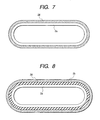
- the conductive member of the present invention may further be of various shapes such as the shape of a sheet, the shape of a belt, the shape of a film and the shape of a plate, as shown in Figs. 5 to 8.
- the layer construction described above may be employed.
- the binder material used to form the surface layer of the conductive member of the present invention may preferably be a resin or an elastomer, and may more preferably be a resin as mentioned above.
- the resin may include fluorine resins, polyamide resins, acrylic resins, polyurethane resins, silicone resins, butyral resins, styrene-ethylene/butylene-olefin copolymers (SEBC) and olefin-ethylene/butylene-olefin copolymers (CEBC).
- SEBC styrene-ethylene/butylene-olefin copolymers
- CEBC olefin-ethylene/butylene-olefin copolymers
- the elastomer may include natural rubbers (which may be vulcanized), synthetic rubbers and thermoplastic elastomers.
- the synthetic rubbers may include EPDM (ethylene-propylene-diene-methylene rubber), SBR (styrene-butadiene rubber), silicone rubber, urethane rubber, IR (isoprene rubber), BR (butadiene rubber), NBR (nitrile-butadiene rubber) and CR (chloroprene rubber).
- EPDM ethylene-propylene-diene-methylene rubber
- SBR styrene-butadiene rubber
- silicone rubber urethane rubber
- IR isoprene rubber
- BR butadiene rubber
- NBR nitrile-butadiene rubber
- CR chloroprene rubber
- the thermoplastic elastomers may include polyolefin type thermoplastic elastomers, urethane type thermoplastic elastomers, polystyrene type thermoplastic elastomers, fluorine rubber type thermoplastic elastomers, polyester type thermoplastic elastomers, polyamide type thermoplastic elastomers, polybutadiene type thermoplastic elastomers, ethylene-vinyl acetate type thermoplastic elastomers, polyvinyl chloride type thermoplastic elastomers and chlorinated polyethylene type thermoplastic elastomers.
- binder materials may be used alone, may be a mixture of two or more types, or may form a copolymer.
- the surface layer 2d is endowed with conductivity by adding conductive fine particles.
- conductive fine particles For the purposes of controlling conductivity, controlling surface properties and improving reinforcing properties, it may further be incorporated with insulating fine particles and different type of conductive fine particles.
- these conductive fine particles and insulating fine particles the fine particles described previously may be used.
- These fine particles may also be those having been subjected to surface treatment, to modification, to introduction of functional groups or molecular chains and to coating, which may be of various types.
- the elastic layer 2b has an appropriate conductivity and elasticity in order to ensure the charging ability to the electrophotographic photosensitive member and the uniform close contact with other members coming into contact with it, such as the electrophotographic photosensitive member.
- the roller in order to ensure the good uniform close contact of the conductive member with other members coming into contact with it, such as the electrophotographic photosensitive member, the roller may preferably be formed into what is called a crown, which is a shape having the largest diameter at the middle and diameters made smaller toward the both ends. It may be formed into the crown by, e.g., sanding the elastic layer 2b.
- the conductive member having the shape of a roller such as the charging roller
- other members coming into contact with it such as the electrophotographic photosensitive member
- the pressure is low at the middle and is larger toward the both ends.
- the conductive member having the shape of a roller has a sufficient straightness. If, however, it has an insufficient straightness, it may cause charge non-uniformity between the middle and the both ends and, corresponding to this non-uniformity, may cause density non-uniformity in images. It is formed into the crown in order to prevent this.
- any materials may be used as long as they are elastomers such as synthetic rubbers and thermoplastic elastomers.
- the elastomers the same elastomers as those described above may be used.
- a foam obtained by foam molding may also be used as the elastic material.
- a synthetic rubber material may preferably be used as the elastic material.
- the elastic layer 2b may preferably be endowed with conductivity to have an electrical resistance adjusted to less than 10 8 ⁇ cm, by adding to the above elastic material the above conductive fine particles or insulating fine particles, or by adding thereto a conducting compound such as an alkali metal salt or an ammonium salt, or by using these in combination. If the elastic layer 2b has an electrical resistance of 10 8 ⁇ cm or more, the conductive member may have a lower charging ability to make it unable to satisfy the charging uniformity to the electrophotographic photosensitive member.
- the elasticity and hardness of the elastic layer 2b may be controlled by adding a softening oil, a plasticizer or the like or by foaming the elastic material.
- the support 2a may at least have conductivity, and a metallic material such as iron, copper, stainless steel, aluminum or nickel may be used.
- a metallic material such as iron, copper, stainless steel, aluminum or nickel
- the metal surface thereof may further be subjected to plating to such an extent that its conductivity is not damaged.
- the surface layer 2d may preferably have an electrical resistance controlled to be higher than the electrical resistance of the elastic layer 2b and to be not higher than 10 16 ⁇ cm. If the surface layer 2d has an electrical resistance lower than that of the elastic layer 2b, it may be unable to prevent leak due to pinholes and scratches of the electrophotographic photosensitive member surface. If it has an electrical resistance higher than 10 16 ⁇ cm, the conductive member (charging member) may have a lower charging ability to make it unable to satisfy charging uniformity.
- the conductive member may be provided with the resistance layer 2c at the position contiguous to the elastic layer 2b, in order that the softening oil or plasticizer contained in the elastic layer can be prevented from bleeding out to the conductive member surface.
- the resistance layer 2c As materials constituting the resistance layer 2c, the same materials as those used in the elastic layer 2b may be used.
- the resistance layer 2c may also preferably have conductivity or semiconductivity.
- the above conductive fine particles of various types As a material which provides conductivity, the above conductive fine particles of various types may be used. In this case, in order to achieve the desired electrical resistance, the above conductive fine particles of various types may be used in combination of two or more.
- the resistance layer 2c may preferably have an electrical resistance controlled to be not higher than the electrical resistance of the surface layer 2d and not lower than the electrical resistance of the elastic layer 2b. If its electrical resistance deviates from this range, it may be unable to satisfy charging uniformity.
- a material having different function may appropriately be used in the elastic layer 2b, the surface layer 2d and the resistance layer 2c.
- a different material may include, in the case of, e.g., the elastic layer 2b, antiaging agents (antioxidants) such as 2-mercaptobenzimidazole, and lubricants such as stearic acid and zinc stearate.
- the elastic layer 2b, the surface layer 2d and the resistance layer 2c may also be subjected to surface treatment.
- the surface treatment may include surface processing treatment making use of ultraviolet rays or electron rays and surface-modifying treatment in which a compound is made to adhere to the surfaces of the layers or the latter is impregnated with the former.
- the electrical resistance (volume resistivity; unit: ⁇ cm) of the elastic layer 2b, surface layer 2d and resistance layer 2c is measured with, e.g., a resistance measuring instrument, an insulation resistance meter HIRESTA-UP, manufactured by Mitsubishi Chemical Corporation.
- the elastic layer material itself is molded into a sheet with a thickness of 2 mm, 250 V of voltage is applied for 30 seconds in an environment of 23°C and 55%RH to measure the volume resistivity.
- the same binder material as that used to form each layer is made into a coating fluid, and its clear coating fluid is coated on an aluminum sheet, where the volume resistivity of each layer is measured under the same conditions as those for the elastic layer 2b.
- the elastic layer 2b, the surface layer 2d and the resistance layer 2c may be formed by any method without any particular limitations as long as it is suited for forming each layer in the desired thickness (with regard to the surface layer, a preferable method of forming it has been described above).
- Known methods concerning layer formation making use of polymeric materials such as resins may be employed.
- These layers may each be formed by bonding a sheetlike or tubelike layer formed previously in a stated thickness, or by covering with the same, or may be formed by, or according to, a conventionally known method such as electrostatic spraying or dipping.
- a method may also be used in which the layers are roughly formed by extrusion and thereafter their shapes are adjusted, or a method in which materials are cured into a stated shape in a mold, followed by forming.
- the elastic layer 2b may preferably have a layer thickness of 0.5 mm or more. If the elastic layer has a layer thickness of less than 0.5 mm, the elastic layer can not have appropriate elasticity, so that its contact with the electrophotographic photosensitive member may come improper to make the conductive member (charging member) not satisfy charging uniformity.
- the surface layer 2d may preferably have a layer thickness of from 1 ⁇ m to 1,000 ⁇ m. If the surface layer has a layer thickness of less than 1 ⁇ m, it tends to have non-uniform layer thickness, and any unevenness of the elastic layer may appear as it is to the surface of the conductive member to make the conductive member (charging member) not satisfy charging uniformity. At the same time, since the surface of the conductive member stands rough (greatly uneven), toner particles and external additives may come to tend to adhere to the conductive member surface. If on the other hand the surface layer is thicker than 1,000 ⁇ m, the appropriate elasticity given to the elastic layer may be lost, so that its contact with the electrophotographic photosensitive member may come improper to make the conductive member (charging member) not satisfy charging uniformity.
- the resistance layer 2c may also preferably have a layer thickness of from 1 ⁇ m to 1,000 ⁇ m.
- layer sections are observed on an optical microscope and their thickness is actually measured. Stated specifically, the conductive member is cut with a cutting knife, and its cut section is observed on an optical or electron microscope and the thickness of each layer is measured.
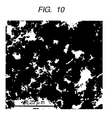
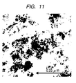
- the particle diameter and average particle diameter of the fine particles 100 particles are picked up at random under observation on a TEM (transmission electron microscope), and the space between two horizontal lines which hold fine particles between them is regarded as the particle diameter of the particles, and its number-based average is regarded as the average particle diameter.
- the area where the fine particles are present is calculated under observation on the transmission electron microscope, and the proportion of the area where the fine particles are present that is held in the whole area is regarded as their content.
- the value measured by connecting MCP-PD41 to LORESTA-GP or HIRESTA-UP is regarded as the volume resistivity of the fine particles.
- the quantity of a sample therefor may preferably appropriately be adjusted according to the density or the like of the fine particles.
- 1.5 g of the sample is weighed in regard to tin oxide, and 0.5 g in regard to carbon black, where applied pressure is set constant at 10.1 MPa (102 kgf/cm 2 ).
- Applied voltage is fixed at 10 V when measured with LORESTA-GP.
- the applied voltage is appropriately changed in accordance with the resistance value to be measured.
- the value of microhardness measured with a microhardness meter MD-1 (manufactured by Kohbunshi Keiki K.K.) is regarded as the hardness.
- the microhardness is what is found when an indenter point (reverse-conical) of 0.16 mm in diameter at the root and 0.5 mm in length is pressed against a sample and the amount of indentation (displacement) of the indenter point at the time of pressing is indicated as hardness value. This enables measurement of the hardness of the surface and its vicinity of the conductive member. Hence, the hardness of materials used in the respective layers can be measured more faithfully.
- the measurement is also made in a peak hold mode in an environment of 23°C/55%RH.
- a sample is molded in the same manner as the sheet sample used to measure the electrical resistance and a measuring terminal is precisely pressed against it, where the value after 5 seconds is read. This is repeated several times, and its average value is regarded as elastic-layer hardness in the present invention.
- the surface layer it is difficult to mold the material into a sheet of 2 mm thick. Accordingly, four sheets of 0.5 mm thick are prepared, and these are superposed together to make a sheet sample of 2 mm thick.
- the value measured in the same manner as the elastic layer is regarded as surface layer hardness in the present invention.
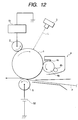
- Fig. 12 is a schematic illustration of the construction of the electrophotographic apparatus of the present invention.
- the electrophotographic apparatus shown in Fig. 12 is an apparatus of a reverse development system utilizing transfer type electrophotography, and is an apparatus having employed the conductive member of the present invention as a charging member.
- Reference numeral 1 denotes a rotating-drum type electrophotographic photosensitive member.
- This electrophotographic photosensitive member 1 is rotatingly driven at a stated peripheral speed (process speed) in the clockwise direction as shown by an arrow in the drawing.
- the process speed is set variable.
- a known electrophotographic photosensitive member may be employed which has a cylindrical support having conductivity and provided on this support a photosensitive layer containing an inorganic photosensitive material or an organic photosensitive material.
- the electrophotographic photosensitive member 1 may further have a charge injection layer for charging the electrophotographic photosensitive member surface to stated polarity and potential.
- Reference numeral 2 denotes a charging roller serving as the charging member (the conducting member of the present invention).
- the charging roller 2 and a charging-bias-applying power source S1 which applies a charging bias to the charging roller 2 constitute a charging means.
- the charging roller 2 is kept in contact with the electrophotographic photosensitive member 1 under a stated pressure. In this apparatus, it is rotatingly driven in the direction following the rotation of the electrophotographic photosensitive member 1. Only a stated DC voltage (in this example, set at -1,200 V) is applied to this charging roller 2 from the charging-bias-applying power source S1, thus the surface of the electrophotographic photosensitive member is electrostatically uniformly charged to stated polarity and potential (in this example, set at a dark-area potential of -600 V).
- Reference numeral 3 denotes an exposure means.
- a known means may be used as the exposure means 3.
- a laser beam scanner is available.
- the surface to be charged is exposed to laser light L corresponding to the intended image information, which is exposed through the exposure means 3, so that the surface potential (set at a light-area potential of -350 V) of the electrophotographic photosensitive member at exposed light areas of the charged surface lowers (attenuates) selectively and an electrostatic latent image is formed on the electrophotographic photosensitive member 1.
- Reference numeral 4 denotes a developing means.
- a known means may be used as the developing means.
- the developing means 4 in this example is so constructed as to have i) a toner-carrying member 4a which is provided at an opening of a developing container holding a toner, and carries and transports the toner, ii) an agitation member 4b which agitates the toner held in the developing container and iii) a toner control member 4c which controls (regulates) the quantity of the toner held on the toner-carrying member 4a (i.e., toner layer thickness).
- a toner (a negative toner) standing charged electrostatically in this example, at a development bias of -350 V) to the same polarity as the charge polarity of the electrophotographic photosensitive member 1 is made to adhere selectively to the exposed light areas of the electrostatic latent image on the electrophotographic photosensitive member surface to render the electrostatic latent image visible as a toner image.
- a developing system there are no particular limitations, and an existent system may be used.
- the existent system may include, e.g., a jumping developing system, a contact developing system and a magnetic-brush developing system.
- the contact developing system is preferred in order to, e.g., prevent the toner from scattering.
- the toner-carrying member 4a used in the contact developing system, it may preferably contain a compound having an elasticity such as rubber, from the viewpoint of ensuring contact stability.
- a developing roller having a support made of a metal or the like and provided thereon an elastic layer endowed with. conductivity may be used.
- This elastic layer may be formed using as an elastic material a foam obtained by foam molding.
- An additional layer may also be provided thereon, or the layer may be subjected to surface treatment.
- the surface treatment may include surface processing treatment making use of ultraviolet rays or electron rays and surface-modifying treatment in which a compound is made to adhere to the layers or the latter is impregnated with the former.
- Reference numeral 5 denotes a transfer roller as a transfer means.
- a known means may be used as the transfer roller 5.
- a transfer roller having a support made of a metal or the like and covered thereon with an elastic resin layer controlled to medium resistance may be used.
- the transfer roller 5 is kept in contact with the electrophotographic photosensitive member 1 under a stated pressure to form a transfer nip, and is rotated in the direction following the rotation of the electrophotographic photosensitive member 1 at a peripheral speed substantially equal to the peripheral speed of the rotation of the electrophotographic photosensitive member 1.
- a transfer voltage having the polarity opposite to the charge polarity of the toner is applied from a transfer bias-applying power source S2.
- a transfer material P is fed at a stated timing from a paper feed mechanism section (not shown) to the transfer nip, and is charged on its back, to the polarity opposite to the charge polarity of the toner by means of a transfer roller 5 to which a transfer voltage is kept applied, whereby the toner image on the side of the electrophotographic photosensitive member 1 surface is electrostatically transferred to the surface side of the transfer material P at the transfer nip.
- the transfer material P to which the toner image has been transferred at the transfer nip is separated from the surface of the electrophotographic photosensitive member 1, and is guided into a toner image fixing means (not shown), where the toner image is subjected to fixing. Then the image-fixed transfer material is put out as an image-formed matter. In the case of a double-side image-forming mode or a multiple-image-forming mode, this image-formed matter is guided into a recirculation delivery mechanism (not shown) and is again guided to the transfer nip.
- Residues on the electrophotographic photosensitive member 1, such as transfer residual toner, are collected from the surface of the electrophotographic photosensitive member 1 by a cleaning means (not shown) which is of, e.g., a blade type. Thereafter, the surface of the electrophotographic photosensitive member 1 is again electrostatically charged by the charging roller 2, and images are repeatedly formed.
- the electrophotographic apparatus in this example may be an apparatus having a process cartridge (not shown) which is so constructed that the electrophotographic photosensitive member 1 and the charging roller 2 are integrally supported by a supporting member such as a resin molded member, and is, in the state of this integral construction, set detachably mountable to the body of the electrophotographic apparatus. It may also be a process cartridge in which not only the electrophotographic photosensitive member 1 and the charging roller 2 but also the developing means 4, the transfer means transfer roller 5 and so forth are integrally supported together.
- the above materials were kneaded for 10 minutes by means of an enclosed mixer adjusted to 50°C, to prepare a raw-material compound.
- a raw-material compound based on 100 parts by weight of the raw-material epichlorohydrin rubber, 1 part by weight of sulfur as a vulcanizing agent, and as vulcanization accelerators 1 part by weight of DM (dibenzothiazyl sulfide) and 0.5 part by weight of TS (tetramethylthiuram monosulfide) were added, and these were kneaded for 10 minutes by means of a twin-roll mill kept cooled to 20°C.
- DM dibenzothiazyl sulfide
- TS tetramethylthiuram monosulfide
- the compound thus obtained was extruded by means of an extruder onto a stainless-steel mandrel of 6 mm in diameter so as to be made into a roller of 15 mm in outer diameter, which was then vulcanized by heating with steam, followed by sanding so as to come to 12 mm in outer diameter to form the elastic layer 2b.
- the roller was in a length of 232 mm.
- the surface layer 2d was formed on the elastic layer to cover it.
- the surface layer 2d was formed by coating the following surface layer coating fluids by dipping. The dipping was carried out twice.
- a liquid mixture was prepared in a container glass bottle, using the following materials.
- Caprolactone-modified acryl-polyol solution 100 parts Methyl isobutyl ketone 250 parts
- Conductive fine tin oxide particles product treated with trifluoropropyltrimethoxysilane; average particle diameter: 0.05 ⁇ m; volume resistivity: 10 3 ⁇ cm
- Hydrophobic fine silica particles product treated with hexamethyldisilazane; average particle diameter: 0.012 ⁇ m; volume resistivity: 10 16 ⁇ cm
- Modified dimethylsilicone oil 0.08 part
- a coating fluid for second-time dipping, a coating fluid was prepared in the same manner as the coating fluid for first-time dipping but using as the fine particles the following particles instead and changing the paint shaker dispersion time to 16 hours.
- Conductive fine tin oxide particles product treated with trifluoropropyltrimethoxysilane; average particle diameter: 0.02 ⁇ m; volume resistivity: 10 3 ⁇ cm
- Hydrophobic fine silica particles product treated with hexamethyldisilazane; average particle diameter: 0.012 ⁇ m; volume resistivity: 10 16 ⁇ cm
- the above surface layer coating solutions were coated by dipping carried out twice.
- draw-up speed the initial speed was set at 16 mm/s, and thereafter the speed was linearly reduced at a rate 1.125 mm/s per second.
- the coating fluid for first-time dipping was coated, followed by air drying at normal temperature for 10 to 30 minutes.
- the roller was reversed, and the coating fluid for second-time dipping was coated in the same manner as the coating fluid for first-time dipping, followed by air drying at normal temperature for 30 minutes or more, and subsequently drying in a circulating hot air dryer at 160°C for 1 hour.
- the surface layer having been dried was in a layer thickness of 15 ⁇ m.
- a section (inclusive of the surface layer) of the charging roller was cured with an acrylic resin, and this was cut with a microtome to prepare slices for transmission electron microscope photography. A transmission electron microscope photograph of this sample was taken and observed to determine average particle diameter by the method described previously.
- Figs. 9 to 11 Part of the transmission electron microscope photograph used to determine the average particle diameter and content is shown in Figs. 9 to 11.
- Fig. 9 shows how the surface layer stands in its total layer thickness;
- Fig. 10 the surface layer lower part;
- Fig. 11 the surface layer upper part.
- the hardness of the elastic layer and surface layer was measured by the method described previously.
- the hardness of the elastic layer was found to be 50°.
- the hardness of the sheet sample prepared using the coating fluid for first-time dipping was 90° and the hardness of the sheet sample prepared using the coating fluid for second-time dipping was 95°; the both being higher than the hardness 50° of the elastic layer.
- the hardness of the whole surface layer can be deemed to be higher than the hardness of the elastic layer.
- the above charging roller was set in the electrophotographic apparatus constructed as shown in Fig. 12, and halftone images were reproduced in each environment of Environment 1 (temperature: 23°C; relative humidity: 55%), Environment 2 (temperature: 32.5°C; relative humidity: 80%) and Environment 3 (temperature: 15°C; relative humidity: 10%).
- the electrophotographic apparatus used in this Example was drivable at process speeds of 94 mm/s and 30 mm/s.
- the images were reproduced also controlling the applied voltage in each environment in such a way that the surface potential V D of the electrophotographic photosensitive member 1 came to -600 V.
- Pinholes of 0.1 mm in diameter and 0.2 mm in diameter were made at the surface of the electrophotographic photosensitive member, and this electrophotographic photosensitive member and the above charging roller were set in the electrophotographic apparatus constructed as shown in Fig. 12, and halftone images were reproduced in each environment in the same manner as in the evaluation of charging uniformity.
- DC -600 V
- AC frequency of 1,000 Hz
- VPP peak-to-peak voltage
- image levels are ranked as follows: Rank 1: no leak is seen on halftone images; Rank 2: leak images of 3 mm or less in diameter are seen on both sides of the pinhole of 0.1 mm in diameter; Rank 3: leak images are seen at the pinhole of 0.1 mm in diameter; and Rank 4: leak images are seen at the pinhole of 0.2 mm in diameter.
- image levels are ranked as follows: Rank 1: no changes from initial-stage images; Rank 2: coarse images (due to slight wear) are slightly seen in halftone images; Rank 3: coarse images and dots (due to slight coming-off of fine particles which is caused by wear) appear slightly in halftone images; and Rank 4: coarse images and dots appear in halftone images.
- the elastic layer was formed in the same manner as in Example 1.
- the surface layer 2d was formed on the elastic layer to cover it.
- the surface layer 2d was formed by coating the following surface layer coating fluid by dipping. The dipping was carried out three times.
- a liquid mixture was prepared in a container glass bottle, using the following materials as materials for the surface layer 2d.
- Caprolactone-modified acryl-polyol solution 100 parts Methyl isobutyl ketone 350 parts
- Conductive fine tin oxide particles product treated with hexyltrimethoxysilane; average particle diameter: 0.10 ⁇ m; volume resistivity: 35 ⁇ cm
- dispersion media glass beads (average particle diameter: 1.0 mm) were so packed as to be in a packing of 70%, followed by dispersion for 7 hours using a paint shaker dispersion machine.
- HDI hexamethylene diisocyanate
- IPDI isophorone diisocyanates
- a coating fluid for third-time dipping a coating fluid was prepared in the same manner as the coating fluid for first-time dipping and second-time dipping but using as the fine particles the following particles instead, changing the dispersion media glass beads for those having an average particle diameter of 0.8 ⁇ m and changing the paint shaker dispersion time to 25 hours.
- Conductive fine tin oxide particles product treated with hexyltrimethoxysilane; average particle diameter: 0.02 ⁇ m; volume resistivity: 20 ⁇ cm
- the above surface layer coating solutions were coated by dipping carried out three times.
- the draw-up speed was fixed to 7 mm/s.
- the coating fluid for first-time dipping was coated, followed by air drying at normal temperature for 10 to 30 minutes.
- the roller was reversed, and the coating fluid for second-time dipping, the same coating fluid as the coating fluid for first-time dipping, was coated in the same manner. Thereafter, this was air-dryed at normal temperature for 10 to 30 minutes, and then the coating fluid for third-time dipping was coated.
- the coating fluid was coated changing the draw-up speed in the same manner as in Example 1.
- the coating thus carried out was followed by air drying at normal temperature for 30 minutes or more, and subsequently drying in a circulating hot air dryer at 160°C for 1 hour.
- the surface layer having been dried was in a layer thickness of 25 ⁇ m.
- the hardness of the sheet sample prepared using the coating fluid for first-time dipping and second-time dipping was 89° and the hardness of the sheet sample prepared using the coating fluid for third-time dipping was 86°; the both being higher than the hardness 50° of the elastic layer.
- the hardness of the whole surface layer can be deemed to be higher than the hardness of the elastic layer.
- the elastic layer was formed in the same manner as in Example 1.
- the surface layer 2d was formed on the elastic layer by carrying out dipping twice.
- the surface layer 2d was formed using twice the same one as the coating fluid for first-time dipping in Example 1.
- the draw-up speed was fixed to 7 mm/s.
- the coating fluid for first-time dipping was coated, followed by air drying at normal temperature for 10 to 30 minutes.
- the coating fluid was allowed to stand also for the same time.
- the roller was reversed, and the same coating fluid as the coating fluid for first-time dipping was coated.
- the coating thus carried out was followed by air drying at normal temperature for 30 minutes or more, and subsequently drying in a circulating hot air dryer at 160°C for 1 hour.
- the surface layer having been dried was in a layer thickness of 20 ⁇ m.
- the hardness of the surface layer was measured in the same manner as in Example 1.
- the hardness of the sheet sample prepared using the coating fluid for dipping was 89°, which was higher than the hardness 50° of the elastic layer.
- the hardness of the whole surface layer can be deemed to be higher than the hardness of the elastic layer.
- the elastic layer was formed in the same manner as in Example 1.
- the surface layer 2d was formed on the elastic layer by carrying out dipping once.
- the surface layer 2d was formed using the same one as the coating fluid for first-time dipping in Example 1.
- the draw-up speed was the same as that in Example 1 except that the initial-stage speed was set at 25 mm/s.
- the coating thus carried out was followed by air drying at normal temperature for 30 minutes or more, and subsequently drying in a circulating hot air dryer at 160°C for 1 hour.
- the surface layer having been dried was in a layer thickness of 18 ⁇ m.
- the hardness of the sheet sample prepared using the coating fluid for dipping was 88°.
- the charging roller in this Example was produced in the same manner as in Example 2 except that, in the coating fluid for first-time dipping and second-time dipping, the conductive fine tin oxide particles were changed for surface-untreated ones (average particle diameter: 0.10 ⁇ m; volume resistivity: 10 ⁇ cm).
- the surface layer having been dried was in a layer thickness of 40 ⁇ m.
- the hardness of the sheet sample prepared using the coating fluid for first-time dipping and second-time dipping was 90° and the hardness of the sheet sample prepared using the coating fluid for third-time dipping was 86°; the both being higher than the hardness 50° of the elastic layer.
- the hardness of the whole surface layer can be deemed to be higher than the hardness of the elastic layer.
- a charging roller was produced in the following way. (by weight) NBR 100 parts Quaternary ammonium salt (the same one as that in Example 1) 4 parts. Calcium carbonate 30 parts Zinc oxide 5 parts Aliphatic acid 2 parts
- the above materials were kneaded for 10 minutes by means of an enclosed mixer adjusted to 50°C, and then further kneaded for 20 minutes by means of an enclosed mixer kept cooled to 20°C to prepare a raw-material compound.
- a raw-material compound based on 100 parts by weight of the raw-material NBR, 1 part by weight of sulfur as a vulcanizing agent and 3 part by weight of NOCCELER TS (as a vulcanization accelerator were added, and these were kneaded for 10 minutes by means of a twin-roll mill kept cooled to 20°C.
- the compound thus obtained was extruded by means of an extruder around the periphery of a stainless-steel mandrel of 6 mm in diameter so as to be made into a roller, which was then vulcanized by heating and shaped by forming, followed by sanding so as to come to 12 mm in outer diameter to form the elastic layer 2b.
- the roller was in a length of 232 mm.
- the surface layer 2d was formed on the elastic layer to cover it.
- the surface layer 2d was formed by coating the following surface layer coating fluids by dipping. The dipping was carried out twice.
- a liquid mixture was prepared by mixing the following materials. (by weight) Caprolactone-modified acryl-polyol solution 100 parts Methyl ethyl ketone 200 parts Carbon black (product treated with hexyltrimethoxysilane; average particle diameter: 0.2 ⁇ m; volume resistivity: 0.1 ⁇ cm) 25 parts
- a coating fluid for second-time dipping a coating fluid was prepared in the same manner as the coating fluid for first-time dipping but changing the carbon black for the following one and changing the bead mill dispersion for that of 100-time circulation. (by weight) Carbon black (product treated with hexyltrimethoxysilane; average particle diameter: 0.06 ⁇ m; volume resistivity: 10 ⁇ cm) 5 parts
- the surface layer was formed by coating in the same manner as in Example 1.
- the surface layer was in a layer thickness of 21 ⁇ m.
- the hardness of the elastic layer and surface layer was measured in the same manner as in Example 1.
- the elastic layer was found to have a hardness of 45°.
- the hardness of the sheet sample prepared using the coating fluid for first-time dipping was 80° and the hardness of the sheet sample prepared using the coating fluid for second-time dipping was 76°; the both being higher than the hardness 45° of the elastic layer.
- the hardness of the whole surface layer can be deemed to be higher than the hardness of the elastic layer.
- the elastic layer was formed in the same manner as in Example 4.
- the surface layer 2d was formed on the elastic layer to cover it.
- the surface layer 2d was formed by coating the following surface layer coating fluids by dipping. The dipping was carried out twice.
- a liquid mixture was prepared by mixing the following materials. (by weight) Polyurethane resin 100 parts Methyl ethyl ketone 200 parts Carbon black (product treated with isopropyltriisostearoyl titanate; average particle diameter: 0.1 ⁇ m; volume resistivity: 1 ⁇ cm) 30 parts
- the above liquid mixture was circulated ten times in this dispersion machine to effect dispersion.
- the surface layer coating fluid for first-time dipping was prepared.
- a liquid mixture was prepared in a container glass bottle, using the following materials.
- Polyurethane resin 100 parts Methyl ethyl ketone 200 parts Conductive fine tin oxide particles (product treated with hexyltrimethoxysilane; average particle diameter: 0.02 ⁇ m; volume resistivity: 20 ⁇ cm) 50 parts
- glass beads (average particle diameter: 0.8 mm) were so packed as to be in a packing of 80%, followed by dispersion for 6 hours using a paint shaker dispersion machine.
- the surface layer was formed by coating in the same manner as in Example 1.
- the surface layer was in a layer thickness of 25 ⁇ m.
- the hardness of the elastic layer and surface layer was measured in the same manner as in Example 1.
- the hardness of the sheet sample prepared using the coating fluid for first-time dipping was 58° and the hardness of the sheet sample prepared using the coating fluid for second-time dipping was 65°; the both being higher than the hardness 50° of the elastic layer.
- the hardness of the whole surface layer can be deemed to be higher than the hardness of the elastic layer.
- the elastic layer was formed in the same manner as in Example 4.
- the surface layer 2d was formed on the elastic layer to cover it.
- the surface layer 2d was formed by coating the following surface layer coating fluids by dipping. The dipping was carried out twice.
- a liquid mixture was prepared in a container glass bottle, using the following materials. (by weight) Polyvinyl butyral resin 100 parts Ethanol 200 parts Carbon black (product treated with isopropyltriisostearoyl titanate; average particle diameter: 0.1 ⁇ m; volume resistivity: 2 ⁇ cm) 50 parts
- glass beads (average particle diameter: 0.8 mm) were so packed as to be in a packing of 50%, followed by dispersion for 0.5 hour using a paint shaker dispersion machine to prepare the coating fluid for first-time dipping.
- a liquid mixture was prepared in a container glass bottle, using the following materials.
- Polyvinyl butyral resin 100 parts Ethanol 200 parts Carbon black (product treated with hexyltrimethoxysilane; average particle diameter: 0.1 ⁇ m; volume resistivity: 10 ⁇ cm) 50 parts
- glass beads (average particle diameter: 0.8 mm) were so packed as to be in a packing of 70%, followed by dispersion for 3 hours using a paint shaker dispersion machine.
- the surface layer was formed by coating in the same manner as in Example 1.
- the surface layer was in a layer thickness of 25 ⁇ m.
- the hardness of the surface layer was measured in the same manner as in Example 1.
- the hardness of the sheet sample prepared using the coating fluid for first-time dipping was 60° and the hardness of the sheet sample prepared using the coating fluid for second-time dipping was 61°; the both being higher than the hardness 50° of the elastic layer.
- the hardness of the whole surface layer can be deemed to be higher than the hardness of the elastic layer.
- a charging roller was produced in the same manner as in Example 4 except that as the fine particles the following particles were used instead in both the coating fluid for first-time dipping and the coating fluid for second-time dipping.
- Fine alumina particles surface-untreated product; average particle diameter: 0.03 ⁇ m; volume resistivity: 10 11 ⁇ cm
- the surface layer was in a layer thickness of 30 ⁇ m.
- the hardness of the surface layer was measured in the same manner as in Example 1.
- the hardness of the sheet sample prepared using the coating fluid for first-time dipping was 81° and the hardness of the sheet sample prepared using the coating fluid for second-time dipping was 78°; the both being higher than the hardness 50° of the elastic layer.
- the hardness of the whole surface layer can be deemed to be higher than the hardness of the elastic layer.
- a charging roller was produced in the same manner as in Example 4 except that as the fine particles the following particles were used instead in both the coating fluid for first-time dipping and the coating fluid for second-time dipping.
- Fine titanium oxide particles product treated with hexyltrimethoxysilane; average particle diameter: 0.03 ⁇ m; volume resistivity: 100 ⁇ cm
- the surface layer was in a layer thickness of 35 ⁇ m.
- the hardness of the surface layer was measured in the same manner as in Example 1.
- the hardness of the sheet sample prepared using the coating fluid for first-time dipping was 76° and the hardness of the sheet sample prepared using the coating fluid for second-time dipping was 72°; the both being higher than the hardness 50° of the elastic layer.
- the hardness of the whole surface layer can be deemed to be higher than the hardness of the elastic layer.
- Example 5 the same evaluation as that in Example 5 was made except that an electrophotographic apparatus drivable at process speeds of 94 mm/s and 47 mm/s was used instead.
- the results are shown in Tables 1 and 2.
- Example 5 the same evaluation as that in Example 5 was made except that an electrophotographic apparatus drivable at process speeds of 94 mm/s and 16 mm/s was used instead.
- the results are shown in Tables 1 and 2.
- a charging roller was produced in the following way. (by weight) EPDM 100 parts Conductive carbon black (surface-untreated product) 20 parts. Zinc oxide 100 parts Aliphatic acid 2 parts
- the above materials were kneaded for 10 minutes by means of an enclosed mixer adjusted to 60°C. Thereafter, based on 100 parts by weight of the EPDM, 15 parts by weight of paraffin oil was added, and these were further kneaded for 20 minutes by means of an enclosed mixer kept cooled to 20°C to prepare a raw-material compound.
- the compound thus obtained was extruded by means of an extruder around the periphery of a stainless-steel mandrel of 6 mm in diameter so as to be made into a roller of 12 mm in outer diameter, which was then vulcanized by heating and shaped by forming to form an elastic layer.
- the roller was in a length of 232 mm.
- a surface layer was formed on the elastic layer by coating the following surface layer coating fluid by dipping. The dipping was carried out once.
- a liquid mixture was prepared in a container glass, using the following materials. (by weight) Polyvinyl butyral resin 100 parts Ethanol 200 parts Carbon black (surface-untreated product; average particle diameter: 0.1 ⁇ m; volume resistivity: 0.8 ⁇ cm) 25 parts
- glass beads (average particle diameter: 0.8 mm) were so packed as to be in a packing of 80%, followed by dispersion for 24 hours using a paint shaker dispersion machine to prepare the surface layer coating fluid.
- the surface layer was formed by coating in the same manner as in Example 1.
- the surface layer was in a layer thickness of 16 ⁇ m.
- the hardness of the elastic layer and surface layer was measured in the same manner as in Example 1.
- the hardness of the elastic layer was 55°, and the hardness of the surface layer was 54°.
- the elastic layer was formed in the same manner as in Comparative Example 1.
- the surface layer of this Comparative Example was formed on the above elastic layer by coating the following surface layer coating fluids by dipping carried out twice.
- Comparative Example 1 As a coating fluid for first-time dipping, the same coating fluid for dipping as that in Comparative Example 1 was used, and was coated in the same manner as Comparative Example 1.
- the surface layer was formed by coating in the same manner as in Example 1.
- the surface layer was in a layer thickness of 40 ⁇ m.
- the hardness of the surface layer was measured in the same manner as in Example 1.
- the hardness of the sheet sample prepared using the coating fluid for first-time dipping was 54° and the hardness of the sheet sample prepared using the coating fluid for second-time dipping was 52°; the both being lower than the hardness 55° of the elastic layer.
- the hardness of the whole surface layer can be deemed to be lower than the hardness of the elastic layer.
- the charging roller in this Comparative Example it was produced in the same manner as in Comparative Example 2 except that in the coating fluid for second-time dipping the carbon black was in an amount of 0 part by weight.
- the hardness of the surface layer was measured in the same manner as in Example 1.
- the hardness of the sheet sample prepared using the coating fluid for first-time dipping was 54° and the hardness of the sheet sample prepared using the coating fluid for second-time dipping was 50°; the both being lower than the hardness 55° of the elastic layer.
- the hardness of the whole surface layer can be deemed to be lower than the hardness of the elastic layer.
- the elastic layer was formed in the same manner as in Comparative Example 1.
- the surface layer of this Comparative Example was formed on the above elastic layer by coating the following surface layer coating fluids by dipping carried out twice.
- a liquid mixture was prepared in a container glass bottle, using the following materials.
- SEBS styrene-ethylene/butylene-styrene
- Methanol 100 parts
- Toluene 100 parts
- Carbon black surface-untreated product; average particle diameter: 0.2 ⁇ m; volume resistivity: 2 ⁇ cm
- glass beads (average particle diameter: 0.8 mm) were so packed as to be in a packing of 50%, followed by dispersion for 0.5 hour using a paint shaker dispersion machine to prepare the coating fluid for first-time dipping.
- a coating fluid for second-time dipping it was prepared in the same manner as the above coating fluid for first-time dipping but using the following materials instead and changing the paint shaker dispersion time to 2 hours.
- SEBS styrene-ethylene/butylene-styrene
- Methanol 100 parts
- Toluene 100 parts
- Carbon black surface-untreated product; average particle diameter: 0.15 ⁇ m; volume resistivity: 2 ⁇ cm
- the surface layer was formed by coating in the same manner as in Example 1.
- the surface layer was in a layer thickness of 32 ⁇ m.
- the hardness of the surface layer was measured in the same manner as in Example 1.
- the hardness of the sheet sample prepared using the coating fluid for first-time dipping was 53° and the hardness of the sheet sample prepared using the coating fluid for second-time dipping was 54°; the both being lower than the hardness 55° of the elastic layer.
- the hardness of the whole surface layer can be deemed to be lower than the hardness of the elastic layer.
- the elastic layer was formed in the same manner as in Comparative Example 1.
- the surface layer of this Comparative Example was formed on the above elastic layer by coating the following surface layer coating fluids by dipping carried out twice.
- a liquid mixture was prepared by mixing the following materials. (by weight) SEBS (styrene-ethylene/butylene-styrene) 100 parts Methanol 100 parts Toluene 100 parts Carbon black (product treated with isopropyltriisostearoyl titanate; average particle diameter: 0.02 ⁇ m; volume resistivity: 0.8 ⁇ cm) 10 parts
- the above liquid mixture was circulated for 72 hours in this dispersion machine to effect dispersion.
- the surface layer coating fluid for first-time dipping was prepared.
- a coating fluid for second-time dipping it was prepared in the same manner as the above coating fluid for first-time dipping but using the following materials instead and changing the dispersion time to 100 hours.
- SEBS styrene-ethylene/butylene-styrene
- Methanol 100 parts
- Toluene 100 parts
- Carbon black surface-untreated product; average particle diameter: 0.15 ⁇ m; volume resistivity: 2 ⁇ cm
- the surface layer was formed by coating in the same manner as in Example 1.
- the surface layer was in a layer thickness of 26 ⁇ m.
- the hardness of the surface layer was measured in the same manner as in Example 1.
- the hardness of the sheet sample prepared using the coating fluid for first-time dipping was 50° and the hardness of the sheet sample prepared using the coating fluid for second-time dipping was 51°; the both being lower than the hardness 55° of the elastic layer.
- the hardness of the whole surface layer can be deemed to be lower than the hardness of the elastic layer.
- the present invention can provide the conductive member which can contribute to the formation of good images over a long period of time even in the electrophotographic apparatus that can set a plurality of different process speed in one machine so as to be adaptable to various kinds of media (transfer materials), and also can be used as a charging member to which only direct-current voltage is applied.
- the present invention can also provide the process cartridge and the electrophotographic apparatus which have the above conductive member as a charging member.
- the cover layer has a surface layer, and the surface layer contains fine particles.
- fine particles present at the surface layer lower part corresponding to a range within 30% of the total layer thickness from the lowermost plane have an average particle diameter which is larger than the average particle diameter of fine particles present at the surface layer upper part corresponding to a range within 30% of the total layer thickness from the uppermost plane.
- a process cartridge and an electrophotographic apparatus have such a conductive member.
Landscapes
- Engineering & Computer Science (AREA)
- Physics & Mathematics (AREA)
- Architecture (AREA)
- Civil Engineering (AREA)
- Structural Engineering (AREA)
- Plasma & Fusion (AREA)
- General Physics & Mathematics (AREA)
- Electrostatic Charge, Transfer And Separation In Electrography (AREA)
- Photoreceptors In Electrophotography (AREA)
- Electrophotography Configuration And Component (AREA)
Priority Applications (1)
| Application Number | Priority Date | Filing Date | Title |
|---|---|---|---|
| EP11181224.4A EP2397916B1 (fr) | 2002-04-19 | 2003-04-16 | Procédé pour produire un élément conducteur |
Applications Claiming Priority (2)
| Application Number | Priority Date | Filing Date | Title |
|---|---|---|---|
| JP2002117323 | 2002-04-19 | ||
| JP2002117323 | 2002-04-19 |
Related Child Applications (1)
| Application Number | Title | Priority Date | Filing Date |
|---|---|---|---|
| EP11181224.4 Division-Into | 2011-09-14 |
Publications (3)
| Publication Number | Publication Date |
|---|---|
| EP1355199A2 true EP1355199A2 (fr) | 2003-10-22 |
| EP1355199A3 EP1355199A3 (fr) | 2006-11-15 |
| EP1355199B1 EP1355199B1 (fr) | 2013-04-10 |
Family
ID=28672678
Family Applications (2)
| Application Number | Title | Priority Date | Filing Date |
|---|---|---|---|
| EP03008919.7A Expired - Lifetime EP1355199B1 (fr) | 2002-04-19 | 2003-04-16 | Elément conducteur, unité de traitement et appareil électrophotographique l'utilisant |
| EP11181224.4A Expired - Lifetime EP2397916B1 (fr) | 2002-04-19 | 2003-04-16 | Procédé pour produire un élément conducteur |
Family Applications After (1)
| Application Number | Title | Priority Date | Filing Date |
|---|---|---|---|
| EP11181224.4A Expired - Lifetime EP2397916B1 (fr) | 2002-04-19 | 2003-04-16 | Procédé pour produire un élément conducteur |
Country Status (4)
| Country | Link |
|---|---|
| US (1) | US6962746B2 (fr) |
| EP (2) | EP1355199B1 (fr) |
| KR (1) | KR100572285B1 (fr) |
| CN (1) | CN100349071C (fr) |
Cited By (5)
| Publication number | Priority date | Publication date | Assignee | Title |
|---|---|---|---|---|
| KR100730679B1 (ko) * | 2003-12-11 | 2007-06-21 | 캐논 가부시끼가이샤 | 현상 장치, 카트리지 및 화상 형성 장치 |
| US8064803B2 (en) | 2006-02-28 | 2011-11-22 | Canon Kabushiki Kaisha | Charging member, process cartridge, and electrophotographic apparatus |
| EP2397916A1 (fr) | 2002-04-19 | 2011-12-21 | Canon Kabushiki Kaisha | Procédé pour produire un élément conducteur |
| EP2345937A4 (fr) * | 2008-10-31 | 2014-04-23 | Canon Kk | Rouleau de charge, cartouche de procédé et dispositif électro-photographique |
| CN112771277A (zh) * | 2019-01-30 | 2021-05-07 | 住友理工株式会社 | 电子照相设备用带电辊 |
Families Citing this family (21)
| Publication number | Priority date | Publication date | Assignee | Title |
|---|---|---|---|---|
| US7054579B2 (en) * | 2003-06-30 | 2006-05-30 | Canon Kabushiki Kaisha | Charging member, process cartridge, and electrophotographic apparatus |
| JP2005283848A (ja) * | 2004-03-29 | 2005-10-13 | Sharp Corp | 帯電器及び画像形成装置 |
| US7937023B2 (en) * | 2004-07-09 | 2011-05-03 | Eastman Kodak Company | Method and a composition for producing an undercoat layer using dialkyl malonate blocked isocyanates (for electrophotographic applications) |
| CN100416421C (zh) * | 2004-08-05 | 2008-09-03 | 佳能株式会社 | 充电部件、处理盒和电子照相装置 |
| JP5183018B2 (ja) * | 2004-08-05 | 2013-04-17 | キヤノン株式会社 | 帯電部材、プロセスカートリッジ及び電子写真装置 |
| WO2006070904A1 (fr) * | 2004-12-28 | 2006-07-06 | Canon Kabushiki Kaisha | Element de charge, cartouche de traitement et appareil electrophotographique |
| JP4679914B2 (ja) * | 2005-01-27 | 2011-05-11 | キヤノン化成株式会社 | 導電性ローラー及び該導電性ローラーを有するプロセスカートリッジ及び電子写真装置 |
| US20080220363A1 (en) * | 2007-03-09 | 2008-09-11 | Konica Minolta Business Technologies, Inc. | Developing roller and image forming method using the same |
| JP2009237463A (ja) * | 2008-03-28 | 2009-10-15 | Konica Minolta Business Technologies Inc | 現像ローラ |
| JP5424795B2 (ja) * | 2008-10-27 | 2014-02-26 | キヤノン株式会社 | 帯電部材及びその製造方法、プロセスカートリッジ及び電子写真装置 |
| JP4455671B1 (ja) * | 2008-11-18 | 2010-04-21 | キヤノン株式会社 | 現像ローラ及びその製造方法、プロセスカートリッジ、電子写真画像形成装置 |
| US8483591B2 (en) * | 2009-08-27 | 2013-07-09 | Xerox Corporation | Bias charging overcoat |
| US8768219B2 (en) * | 2009-11-20 | 2014-07-01 | Xerox Corporation | Bias charging overcoat |
| US8649704B2 (en) * | 2009-11-20 | 2014-02-11 | Xerox Corporation | Bias charging overcoat |
| US9500555B2 (en) * | 2010-01-19 | 2016-11-22 | Clark Robert Gunness | Method and system for leak detection in roofing and waterproofing membranes |
| JP4942233B2 (ja) * | 2010-09-27 | 2012-05-30 | キヤノン株式会社 | 帯電部材、プロセスカートリッジおよび電子写真装置 |
| KR101543139B1 (ko) * | 2011-02-15 | 2015-08-07 | 캐논 가부시끼가이샤 | 대전 부재, 그 제조 방법, 프로세스 카트리지 및 전자 사진 장치 |
| JP6053354B2 (ja) * | 2011-07-06 | 2016-12-27 | キヤノン株式会社 | 帯電部材とその製造方法、および電子写真装置 |
| JP6067632B2 (ja) | 2013-11-21 | 2017-01-25 | 三星電子株式会社Samsung Electronics Co.,Ltd. | 帯電部材 |
| US9360789B1 (en) * | 2014-11-28 | 2016-06-07 | Canon Kabushiki Kaisha | Member for electrophotography, process cartridge and image forming apparatus |
| JP2017025213A (ja) * | 2015-07-23 | 2017-02-02 | 富士ゼロックス株式会社 | 画像形成装置用表面処理カーボンブラック、画像形成装置用管状体、画像形成装置用管状体ユニット、及び画像形成装置 |
Citations (2)
| Publication number | Priority date | Publication date | Assignee | Title |
|---|---|---|---|---|
| JP2000039755A (ja) | 1998-07-24 | 2000-02-08 | Hokushin Ind Inc | 導電部材 |
| JP2001209235A (ja) | 2000-01-25 | 2001-08-03 | Hokushin Ind Inc | 導電部材 |
Family Cites Families (9)
| Publication number | Priority date | Publication date | Assignee | Title |
|---|---|---|---|---|
| JP2759510B2 (ja) * | 1989-07-28 | 1998-05-28 | キヤノン株式会社 | 現像剤及び画像形成方法 |
| JPH0387843A (ja) | 1989-08-31 | 1991-04-12 | Canon Inc | 画像形成装置 |
| JP3575054B2 (ja) * | 1994-04-22 | 2004-10-06 | 東海ゴム工業株式会社 | 導電性ロールの製造方法 |
| JP3376289B2 (ja) * | 1998-09-04 | 2003-02-10 | キヤノン株式会社 | 帯電部材、帯電方法、帯電装置、画像形成装置、及びプロセスカートリッジ |
| US6035163A (en) * | 1998-11-20 | 2000-03-07 | Xerox Corporation | Vibration absorbing bias charge roll |
| US6558781B1 (en) | 1999-07-12 | 2003-05-06 | Canon Kabushiki Kaisha | Conductive roller, process cartridge and image forming apparatus |
| US6337962B1 (en) | 1999-08-12 | 2002-01-08 | Canon Kabushiki Kaisha | Process cartridge and electrophotographic apparatus |
| EP1089132B1 (fr) * | 1999-09-30 | 2008-10-08 | Canon Kabushiki Kaisha | Méthode de production d'un elément conducteur pour un appareil de formation d'images |
| US6962746B2 (en) | 2002-04-19 | 2005-11-08 | Canon Kasei Kabushiki Kaisha | Conductive member, and process cartridge and electrophotographic apparatus which make use of the same |
-
2003
- 2003-04-10 US US10/410,299 patent/US6962746B2/en not_active Expired - Lifetime
- 2003-04-16 EP EP03008919.7A patent/EP1355199B1/fr not_active Expired - Lifetime
- 2003-04-16 EP EP11181224.4A patent/EP2397916B1/fr not_active Expired - Lifetime
- 2003-04-17 CN CNB031221432A patent/CN100349071C/zh not_active Expired - Fee Related
- 2003-04-19 KR KR1020030024874A patent/KR100572285B1/ko not_active Expired - Fee Related
Patent Citations (2)
| Publication number | Priority date | Publication date | Assignee | Title |
|---|---|---|---|---|
| JP2000039755A (ja) | 1998-07-24 | 2000-02-08 | Hokushin Ind Inc | 導電部材 |
| JP2001209235A (ja) | 2000-01-25 | 2001-08-03 | Hokushin Ind Inc | 導電部材 |
Cited By (6)
| Publication number | Priority date | Publication date | Assignee | Title |
|---|---|---|---|---|
| EP2397916A1 (fr) | 2002-04-19 | 2011-12-21 | Canon Kabushiki Kaisha | Procédé pour produire un élément conducteur |
| KR100730679B1 (ko) * | 2003-12-11 | 2007-06-21 | 캐논 가부시끼가이샤 | 현상 장치, 카트리지 및 화상 형성 장치 |
| US8064803B2 (en) | 2006-02-28 | 2011-11-22 | Canon Kabushiki Kaisha | Charging member, process cartridge, and electrophotographic apparatus |
| EP2345937A4 (fr) * | 2008-10-31 | 2014-04-23 | Canon Kk | Rouleau de charge, cartouche de procédé et dispositif électro-photographique |
| CN112771277A (zh) * | 2019-01-30 | 2021-05-07 | 住友理工株式会社 | 电子照相设备用带电辊 |
| CN112771277B (zh) * | 2019-01-30 | 2023-02-17 | 住友理工株式会社 | 电子照相设备用带电辊 |
Also Published As
| Publication number | Publication date |
|---|---|
| CN1453651A (zh) | 2003-11-05 |
| US20030219589A1 (en) | 2003-11-27 |
| CN100349071C (zh) | 2007-11-14 |
| US6962746B2 (en) | 2005-11-08 |
| KR100572285B1 (ko) | 2006-04-19 |
| KR20040021504A (ko) | 2004-03-10 |
| EP1355199B1 (fr) | 2013-04-10 |
| EP1355199A3 (fr) | 2006-11-15 |
| EP2397916A1 (fr) | 2011-12-21 |
| EP2397916B1 (fr) | 2013-04-10 |
Similar Documents
| Publication | Publication Date | Title |
|---|---|---|
| EP2397916B1 (fr) | Procédé pour produire un élément conducteur | |
| US5978639A (en) | Intermediate transfer member and intermediate transfer device | |
| EP2667258B1 (fr) | Rouleau de développement, dispositif de développement et dispositif de formation d'image | |
| US6400919B1 (en) | Conducting member, process cartridge and image-forming apparatus | |
| EP1624347B1 (fr) | Elément de chargement, cartouche de traitement et appareil électrophotographique | |
| JP2010086003A (ja) | 帯電部材、プロセスカートリッジおよび電子写真装置 | |
| CN102002227A (zh) | 用于导电辊的组合物、导电辊、充电单元、成像装置、处理盒、以及制造导电辊的方法 | |
| JP2008129481A (ja) | 画像形成用半導電性部材、並びに画像形成装置、画像形成方法、及びプロセスカートリッジ | |
| JP4328554B2 (ja) | 導電性部材、これを用いた電子写真装置およびプロセスカートリッジ | |
| KR20210091622A (ko) | 대전 부재 및 이를 채용한 전자사진 화상 형성 장치 | |
| JP4227448B2 (ja) | 導電性部材、画像形成装置及びプロセスカートリッジ | |
| JP4473298B2 (ja) | 導電性部材の製造方法 | |
| HK1059830A (en) | Conductive member, and process cartridge and electrophotographic apparatus which make use of the same | |
| JP2005037931A (ja) | 帯電部材、プロセスカートリッジおよび電子写真装置 | |
| HK1159763A (en) | Process for producing a conductive member | |
| JP2005315979A (ja) | 導電性部材、プロセスカートリッジ及び画像形成装置 | |
| JP5178073B2 (ja) | 帯電部材及び帯電装置 | |
| JP2006113377A (ja) | 帯電部材、これを用いたプロセスカートリッジ及び電子写真装置 | |
| US20080124130A1 (en) | Charging device, image forming apparatus and charging method | |
| JP4217578B2 (ja) | 帯電部材、これを用いたプロセスカートリッジ及び電子写真装置 | |
| JP2005165213A (ja) | 帯電部材、画像形成装置、帯電方法及びプロセスカートリッジ | |
| JP2024083236A (ja) | プロセスカートリッジおよび画像形成装置 | |
| JP5776245B2 (ja) | 導電性部材、帯電装置、プロセスカートリッジおよび画像形成装置 | |
| JP2006234898A (ja) | 導電性部材の製造方法及び電子写真用導電性部材 | |
| JP2008026400A (ja) | プロセスカートリッジ及び画像形成装置 |
Legal Events
| Date | Code | Title | Description |
|---|---|---|---|
| PUAI | Public reference made under article 153(3) epc to a published international application that has entered the european phase |
Free format text: ORIGINAL CODE: 0009012 |
|
| AK | Designated contracting states |
Kind code of ref document: A2 Designated state(s): AT BE BG CH CY CZ DE DK EE ES FI FR GB GR HU IE IT LI LU MC NL PT RO SE SI SK TR |
|
| AX | Request for extension of the european patent |
Extension state: AL LT LV MK |
|
| RIN1 | Information on inventor provided before grant (corrected) |
Inventor name: INOUE, HIROSHI Inventor name: KURODA, NORIAKI Inventor name: DOI, SHINJI Inventor name: IKEDA, ATSUSHI,C/O CANON KASEI KABUSHIKI KAISHA Inventor name: OTAKA, TOSHIHIRO,C/O CANON KASEI KABUSHIKI KAISHA Inventor name: KATO, HISAO Inventor name: TSURU, SEIJI Inventor name: OSADA, HIROYUKI Inventor name: TANIGUCHI, TOMOHITO |
|
| REG | Reference to a national code |
Ref country code: HK Ref legal event code: DE Ref document number: 1059830 Country of ref document: HK |
|
| PUAL | Search report despatched |
Free format text: ORIGINAL CODE: 0009013 |
|
| AK | Designated contracting states |
Kind code of ref document: A3 Designated state(s): AT BE BG CH CY CZ DE DK EE ES FI FR GB GR HU IE IT LI LU MC NL PT RO SE SI SK TR |
|
| AX | Request for extension of the european patent |
Extension state: AL LT LV MK |
|
| 17P | Request for examination filed |
Effective date: 20070514 |
|
| AKX | Designation fees paid |
Designated state(s): DE FR GB IT |
|
| 17Q | First examination report despatched |
Effective date: 20090914 |
|
| GRAP | Despatch of communication of intention to grant a patent |
Free format text: ORIGINAL CODE: EPIDOSNIGR1 |
|
| GRAS | Grant fee paid |
Free format text: ORIGINAL CODE: EPIDOSNIGR3 |
|
| GRAA | (expected) grant |
Free format text: ORIGINAL CODE: 0009210 |
|
| AK | Designated contracting states |
Kind code of ref document: B1 Designated state(s): DE FR GB IT |
|
| REG | Reference to a national code |
Ref country code: GB Ref legal event code: FG4D Ref country code: DE Ref legal event code: R081 Ref document number: 60343708 Country of ref document: DE Owner name: CANON KABUSHIKI KAISHA, JP Free format text: FORMER OWNER: CANON K.K., CANON KASEI K.K., , JP Ref country code: DE Ref legal event code: R081 Ref document number: 60343708 Country of ref document: DE Owner name: CANON KABUSHIKI KAISHA, JP Free format text: FORMER OWNERS: CANON K.K., TOKYO, JP; CANON KASEI K.K., TSUKUBA, JP |
|
| REG | Reference to a national code |
Ref country code: DE Ref legal event code: R096 Ref document number: 60343708 Country of ref document: DE Effective date: 20130613 |
|
| REG | Reference to a national code |
Ref country code: HK Ref legal event code: WD Ref document number: 1059830 Country of ref document: HK |
|
| PLBE | No opposition filed within time limit |
Free format text: ORIGINAL CODE: 0009261 |
|
| STAA | Information on the status of an ep patent application or granted ep patent |
Free format text: STATUS: NO OPPOSITION FILED WITHIN TIME LIMIT |
|
| 26N | No opposition filed |
Effective date: 20140113 |
|
| REG | Reference to a national code |
Ref country code: DE Ref legal event code: R097 Ref document number: 60343708 Country of ref document: DE Effective date: 20140113 |
|
| PGFP | Annual fee paid to national office [announced via postgrant information from national office to epo] |
Ref country code: GB Payment date: 20140416 Year of fee payment: 12 |
|
| PGFP | Annual fee paid to national office [announced via postgrant information from national office to epo] |
Ref country code: IT Payment date: 20140418 Year of fee payment: 12 Ref country code: FR Payment date: 20140409 Year of fee payment: 12 |
|
| REG | Reference to a national code |
Ref country code: DE Ref legal event code: R082 Ref document number: 60343708 Country of ref document: DE Representative=s name: TBK, DE Ref country code: DE Ref legal event code: R081 Ref document number: 60343708 Country of ref document: DE Owner name: CANON KABUSHIKI KAISHA, JP Free format text: FORMER OWNER: CANON KABUSHIKI KAISHA, CANON KASEI K.K., , JP Ref country code: DE Ref legal event code: R081 Ref document number: 60343708 Country of ref document: DE Owner name: CANON KABUSHIKI KAISHA, JP Free format text: FORMER OWNERS: CANON KABUSHIKI KAISHA, TOKYO, JP; CANON KASEI K.K., TSUKUBA, JP |
|
| GBPC | Gb: european patent ceased through non-payment of renewal fee |
Effective date: 20150416 |
|
| PG25 | Lapsed in a contracting state [announced via postgrant information from national office to epo] |
Ref country code: IT Free format text: LAPSE BECAUSE OF NON-PAYMENT OF DUE FEES Effective date: 20150416 Ref country code: GB Free format text: LAPSE BECAUSE OF NON-PAYMENT OF DUE FEES Effective date: 20150416 |
|
| REG | Reference to a national code |
Ref country code: FR Ref legal event code: ST Effective date: 20151231 |
|
| PG25 | Lapsed in a contracting state [announced via postgrant information from national office to epo] |
Ref country code: FR Free format text: LAPSE BECAUSE OF NON-PAYMENT OF DUE FEES Effective date: 20150430 |
|
| PGFP | Annual fee paid to national office [announced via postgrant information from national office to epo] |
Ref country code: DE Payment date: 20210323 Year of fee payment: 19 |
|
| REG | Reference to a national code |
Ref country code: DE Ref legal event code: R119 Ref document number: 60343708 Country of ref document: DE |
|
| PG25 | Lapsed in a contracting state [announced via postgrant information from national office to epo] |
Ref country code: DE Free format text: LAPSE BECAUSE OF NON-PAYMENT OF DUE FEES Effective date: 20221103 |