EP1355416B1 - CMOS high impedance circuit - Google Patents
CMOS high impedance circuit Download PDFInfo
- Publication number
- EP1355416B1 EP1355416B1 EP03076181A EP03076181A EP1355416B1 EP 1355416 B1 EP1355416 B1 EP 1355416B1 EP 03076181 A EP03076181 A EP 03076181A EP 03076181 A EP03076181 A EP 03076181A EP 1355416 B1 EP1355416 B1 EP 1355416B1
- Authority
- EP
- European Patent Office
- Prior art keywords
- circuit
- mosfet device
- channel
- input
- impedance
- Prior art date
- Legal status (The legal status is an assumption and is not a legal conclusion. Google has not performed a legal analysis and makes no representation as to the accuracy of the status listed.)
- Expired - Lifetime
Links
Images




Classifications
-
- H—ELECTRICITY
- H03—ELECTRONIC CIRCUITRY
- H03F—AMPLIFIERS
- H03F3/00—Amplifiers with only discharge tubes or only semiconductor devices as amplifying elements
- H03F3/181—Low-frequency amplifiers, e.g. audio preamplifiers
-
- H—ELECTRICITY
- H03—ELECTRONIC CIRCUITRY
- H03F—AMPLIFIERS
- H03F1/00—Details of amplifiers with only discharge tubes, only semiconductor devices or only unspecified devices as amplifying elements
- H03F1/30—Modifications of amplifiers to reduce influence of variations of temperature or supply voltage or other physical parameters
- H03F1/301—Modifications of amplifiers to reduce influence of variations of temperature or supply voltage or other physical parameters in MOSFET amplifiers
Definitions
- a hearing aid utilizes three basic components, a microphone, an amplifier and a receiver or loudspeaker component.
- the microphone generally includes a transducer for converting incoming sound pressure levels to corresponding electrical signals.
- the amplifier amplifies these electrical signals to a desired level, and the receiver or loudspeaker component translates these amplified electrical signals to an acoustical sound output, or outgoing sound pressure level.
- the microphone component includes a transducer such as an electret microphone, and a buffer amplifier or "preamplifier.”
- a CMOS amplifier component is used as the preamplifier, e.g. as disclosed in US 5 861 779 and JP 08 182 092 .
- the input of this CMOS preamplifier must be biased to ground level.
- the impedance of the preamplifier input should be relatively large, and preferably, as large as possible.
- bias resistor values of about 10 Gohms are utilized. For further noise reduction, this value might be increased up to 100 Gohms.
- resistors cannot be implemented on ICs but must be made on a thick film hybrid.
- a pair of small diodes coupled in parallel but in opposite polarity i.e., "antiparallel" are sometimes used. This permits a relatively large impedance value to be obtained, which value is strongly dependant upon process variations.
- diodes for this purpose has the disadvantages of slow settling and slow overload recovery, which are characteristics of diodes.
- the bias voltage for the input of a preamplifier is supplied through a high-ohmic resistance or through a pair of anti-parallel diodes.
- the impedance of such device must be very high.
- the impedance has a certain maximum level, in order to enable a fast startup of the amplifier, and a fast recovery after overload.
- An integrated diode pair forms too high an impedance for guaranteeing stability; however, adding a parallel resistor (10-100 Gohms) introduces a level of noise.
- a high impedance input circuit for a buffer amplifier/preamplifier of a hearing aid microphone comprises a CMOS transistor circuit coupled across an input of said buffer amplifier/preamplifier and providing a high impedance.
- a high impedance input circuit for a buffer amplifier/preamplifier of a hearing aid microphone comprises a diode-connected MOSFET circuit.
- a high impedance circuit comprises a CMOS transistor circuit providing a high impedance equivalent to a pair of antiparallel diodes.
- a high impedance circuit comprises a diode-connected MOSFET circuit.
- a method of constructing a high impedance circuit comprises forming on an integrated chip at least one p-channel transistor and at least one n-channel transistor coupled in circuit to provide a diode-switched high impedance.
- a schematic circuit diagram of a microphone 10 for a hearing aid is designated generally by the reference numeral 10.
- the microphone includes a transducer component 12 such as an electret microphone which is symbolized in FIG. 1 as a current source.
- the microphone 10 also includes a buffer amplifier/preamplifier circuit portion 14 (hereinafter “preamplifier”)which may comprise an MOS field effect transistor (FET) 16 wired in a common source configuration.
- FET MOS field effect transistor
- a positive voltage 18 is provided with a suitable biasing resistor 19 for the transistor 16.
- a common or negative voltage connection 20 is also provided.
- the source electrode of the FET 16 provides the output 22 of the preamplifier 14.
- the preamplifier circuit 14 may be realized on a single integrated circuit (IC) chip 15.
- the input of the preamplifier 14 for the microphone 10 must be biased to ground level. Since the signal source in the electret 12 is a very small capacitor, the impedance of the amplifier input must be as large as possible. Currently, a bias resistor 24 of about 10 Gohms is used. For reasons of noise reduction this value may be increased up to 100 Gohms. These resistors cannot be realized on IC's, therefore they are usually made on a thick film hybrid.
- FIG. 2 a similar microphone 10 employing an electret transducer or microphone 12 and a preamplifier circuit 14, on an IC chip 15, is illustrated. Like reference numerals are utilized to designate like elements in FIG. 2 .
- the input impedance for the preamplifier 14 may be integrated onto the same chip 15 in the form of a pair of parallel diodes 26, 28 connected in reverse polarity.
- a relatively large impedance value can be obtained by the use of such diodes 26, 28, however, the value is strongly dependant on process variations. That is, it is difficult in the integrated circuit manufacture process to accurately predict the value of the impedance obtained by use of diodes 26, 28 within acceptable tolerance levels.
- the diodes 26, 28 also exhibit properties typical of diodes, in that they are relatively slow in settling of the voltage over the diode or reaching steady state conditions, exhibit relatively slow overload recovery times, and the like.
- the input impedance in FIG. 3 is provided by an additional CMOS transistor or MOSFET circuit 30.
- the MOSFET circuit 30 is used as a high impedance transconductance.
- the MOS transistor circuit 30 may be integrated by CMOS technology onto the same chip 15 as the preamplifier circuit 14.
- the components of circuit 30 may be integrated on the same chip with the existing components of FIG. 2 , with the circuit 30 in parallel with the diodes 26, 28. This approach affords some economy in that the entire chip does not have to be redesigned and refabricated.
- the specifications of the MOSFET circuit 30 are such that the influence of the diodes 26, 28 on its performance is negligible.
- the chip may be fabricated without the diodes 26, 28, if desired.
- the MOSFET circuit 30 is designed so that the impedance is always higher than some selected minimum value, e.g. 50-100 Gohms, at the minimum control voltage.
- MOSFETs 90, 92, 94, 96 are used. Both p-channel 90, 92 and n-channel 94, 96 devices are used in the configuration shown in order to obtain symmetry.
- the circuit of four MOSFETS may be parallel with a diode pair 26, 28 of FIG. 2 , as noted above.
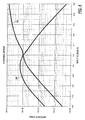
- the graph of FIG. 4 shows the impedance curve of two ways to connect an n-channel device.
- the curve marked 100 is the impedance of the n-channel device 96 of FIG. 3
- the curve marked 102 is the impedance of the n-channel device 94 of FIG. 3 .
- the bulk connections are all grounded.
- the impedance of the parallel connection of both n-channels devices ( FIG. 6 ) is almost symmetrical for positive and negative input voltages.
- the graph of FIG. 5 shows the impedance curves of two ways to connect a p-channel device.
- the curve marked 104 is the impedance of the p-channel device 92 of FIG. 3
- the curve marked 106 is the impedance of the p-channel device 90 of FIG. 3 .
- the impedance of the parallel connection of both p-channels devices ( FIG. 7 ) is almost symmetrical for positive and negative input voltages, and is a mirror image compared with the n-channels graph of FIG. 6 .
- FIGS. 5 and 7 show the same behavior, and are mirror images compared with the n-channels graphs of FIGS. 4 and 6 .
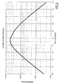
- the graph of FIG. 8 shows the impedance of the series connection of the n-channel pair and the p-channel pair of FIG. 3 .
- This graph is symmetrical.
- the devices are scaled, so that the impedance at zero bias voltage is at the desired level. At this point, all devices contribute to the total impedance equally, so that the sensitivity of the impedance due to component variation is minimal.
- the circuitry of the invention can be integrated onto a common chip with the buffer amplifier/preamplifier circuitry. Unlike the diodes utilized in the embodiment of FIG. 2 , the circuit of the invention is relatively insensitive to process variations in the IC manufacture process.
- the extremely high impedance which can be achieved by the circuitry of the invention minimizes the noise figure and optimizes signal to noise ratio of the microphone component including the electret 12 and preamplifier 14. Also, the controlled impedance of the invention further limits and minimizes input settling time of the buffer amplifier circuitry 14.
- the design is dimensioned, depending on the characteristics of the CMOS process, in such a way that the minimum impedance (i.e., with the minimum occurring threshold voltages) of the circuit is about 100 Gohms.
- the maximum impedance is about a factor of 10 higher.
- the impedance is more stable for process variations than the impedance of the anti-parallel diodes.
- the circuit is much simpler and requires much less chip area than the advanced "high impedance bias device.”
- the additional parasitic capacitance is very small (since the sizes of the MOSFETs are very small, and only small diffusion areas are connected to the signal input).
- the circuit can also be placed in parallel with the anti-parallel diodes (in order to cover a wider range of process variations).
- the circuit is passive, no risk for oscillation and no battery/current consumption.
- Linearity is very good for signals up to 300 mV amplitude.
- CMOS high impedance circuit has been described above with reference to its use as a high input impedance bias circuit for a CMOS preamplifier, such as in a hearing aid, it has many other uses.
- CMOS high impedance circuit is a simple, very powerful passive circuit that can be applied everywhere there is a need for a high impedance, low noise circuit.
- a high input impedance input circuit for a buffer amplifier/preamplifier of a hearing aid microphone said high input impedance circuit comprising: a CMOS transistor circuit providing an impedance equivalent to a pair of antiparallel diodes connected between an input of said buffer amplifier and a reference voltage.
- Said transistor circuit may be integrated on a single integrated circuit chip with said buffer amplifier/preamplifier.
- Said high impedance circuit may comprises at least one p-channel MOSFET device or at least one n-channel MOSFET device, wherein a drain terminal of said MOSFET device is connected with said buffer amplifier input, and all other terminals of said MOSFET device are connected with said reference voltage.
- said high impedance circuit may comprises at least one p-channel MOSFET device or at least one n-channel MOSFET device, and wherein drain and gate terminals of said MOSFET device are connected with said buffer amplifier input, and source and bulk terminals of said MOSFET device are connected with said reference voltage.
- said high impedance circuit may comprise a parallel connection of at least one first circuit and at least one second circuit, said first circuit comprising at least one p-channel MOSFET device and at least one n-channel MOSFET device, wherein a drain terminal of said MOSFET device is connected with said buffer amplifier input, and all other terminals of said MOSFET device are connected with said reference voltage and said second circuit comprising at least one p-channel MOSFET device or at least one n-channel MOSFET device, wherein drain and gate terminals of said MOSFET device are connected with said buffer amplifier input, and source and bulk terminals of said MOSFET device are connected with said reference voltage.
- said high impedance circuit may comprise the series connection of at least one first circuit and at least one second circuit, said first circuit being connected between said buffer amplifier input and a common node between said first circuit and said second circuit, and said second circuit being connected between said common node and said reference voltage, wherein said first circuit comprises a parallel connection of at least one third circuit and at least one fourth circuit, said third circuit comprising at least one p-channel MOSFET device or at least one n-channel MOSFET device, wherein a drain terminal of said MOSFET device is connected with said buffer amplifier input, and all other terminals of said MOSFET device are connected with said common node, and said fourth circuit comprising at least one p-channel MOSFET device or at least one n-channel MOSFET device, wherein drain and gate terminals of said MOSFET device are connected with said buffer amplifier input, and source and bulk terminals of said MOSFET device are connected with said common node, said second circuit comprises a parallel connection of at least one fifth circuit and at least one sixth circuit, said fifth circuit comprising of
- the invention further relates to a method of constructing high input impedance input circuit for a buffer amplifier/preamplifier of a hearing aid microphone on a single integrated circuit chip with said buffer amplifier/preamplifier said method comprising: forming on said integrated circuit chip at least one p-channel transistor or at least one n-channel transistor coupled across an input of said buffer amplifier/preamplifier and providing a high impedance.
- said high impedance may comprise a symmetrical high impedance.
- Said forming at least one transistor may comprise forming a diode-connected MOS component.
- Said forming at least one transistor may include forming at least one p-channel MOSFET device or at least one n-channel MOSFET device, connecting a drain terminal of said MOSFET device with an input of said buffer amplifier and connecting all other terminals of said MOSFET device with a reference voltage.
- Said forming furthermore may include forming at least one p-channel MOSFET device or at least one n-channel MOSFET device, connecting drain and gate terminals of said MOSFET device with an input of said buffer amplifier and connecting source and bulk terminals of said MOSFET device with a reference voltage.
- said forming may comprise forming at least one first p-channel MOSFET device and at least one first n-channel MOSFET device, connecting a drain terminal of said first MOSFET device with an input of said buffer amplifier and connecting all other terminals of said first MOSFET device with a reference voltage, and forming at least one second p-channel MOSFET device or at least one second n-channel MOSFET device, connecting drain and gate terminals of said second MOSFET device with an input of said buffer amplifier and connecting source and bulk terminals of said second MOSFET device with a reference voltage and connecting said first and second device in parallel.
- said forming said circuit may comprise forming the series connection of at least one first circuit and at least one second circuit, said first circuit being connected between said buffer amplifier input and a common node between said first circuit and said second circuit, and said second circuit being connected between said common node and said reference voltage, said first circuit comprises a parallel connection of at least one third circuit and at least one fourth circuit, said third circuit comprising at least one p-channel MOSFET device or at least one n-channel MOSFET device, wherein a drain terminal of said MOSFET device is connected with said buffer amplifier input, and all other terminals of said MOSFET device are connected with said common node, and said fourth circuit comprising at least one p-channel MOSFET device or at least one n-channel MOSFET device, wherein drain and gate terminals of said MOSFET device are connected with said buffer amplifier input, and source and bulk terminals of said MOSFET device are connected with said common node, said second circuit comprises a parallel connection of at least one fifth circuit and at least one sixth circuit, said fifth circuit comprising at least
- the invention is further characterized by a high input impedance input circuit for a buffer amplifier/preamplifier of a hearing aid microphone, said high input impedance circuit comprising a diode-connected MOSFET circuit.
- Said MOSFET circuit may comprise at least one p-channel transistor or at least one n-channel transistor.
- Said MOSFET circuit may comprise two or more p-channel and/or n-channel transistors coupled in parallel or in series.
- Said MOSFET circuit may include said high impedance circuit comprises at least one p-channel MOSFET device or at least one n-channel MOSFET device, and wherein a drain terminal of said MOSFET device is connected with said buffer amplifier input, and all other terminals of said MOSFET device are connected with said reference voltage.
- Said MOSFET circuit may include said high impedance circuit comprising at least one p-channel MOSFET device or at least one n-channel MOSFET device, and wherein drain and gate terminals of said MOSFET device are connected with said buffer amplifier input, and source and bulk terminals of said MOSFET device are connected with said reference voltage.
- said high impedance circuit may comprise a parallel connection of at least one first circuit and at least one second circuit, said first circuit comprising at least one p-channel MOSFET device and at least one n-channel MOSFET device, wherein a drain terminal of said MOSFET device is connected with said buffer amplifier input, and all other terminals of said MOSFET device are connected with said reference voltage and said second circuit comprising at least one p-channel MOSFET device or at least one n-channel MOSFET device, wherein drain and gate terminals of said MOSFET device are connected with said buffer amplifier input, and source and bulk terminals of said MOSFET device are connected with said reference voltage.
- Said high impedance circuit may comprise the series connection of at least one first circuit and at least one second circuit, said first circuit being connected between said buffer amplifier input and a common node between said first circuit and said second circuit, and said second circuit being connected between said common node and said reference voltage, wherein said first circuit comprises a parallel connection of at least one third circuit and at least one fourth circuit, said third circuit comprising at least one p-channel MOSFET device or at least one n-channel MOSFET device, wherein a drain terminal of said MOSFET device is connected with said buffer amplifier input, and all other terminals of said MOSFET device are connected with said common node, and said fourth circuit comprising at least one p-channel MOSFET device or at least one n-channel MOSFET device, wherein drain and gate terminals of said MOSFET device are connected with said buffer amplifier input, and source and bulk terminals of said MOSFET device are connected with said common node, said second circuit comprises a parallel connection of at least one fifth circuit and at least one sixth circuit, said fifth circuit comprising
- the invention is regards a high input impedance circuit comprising a diode connected MOSFET circuit.
- Said MOSFET circuit may comprise a CMOS circuit providing an impedance equivalent to a pair of antiparallel diodes.
- Said MOSFET circuit may be integrated on a single integrated circuit chip.
- Said MOSFET circuit may comprise at least one p-channel transistor device or at least one n-channel transistor device.
- said MOSFET circuit may include said high impedance circuit comprising at least one p-channel MOSFET device or at least one n-channel MOSFET device, and wherein a drain terminal of said MOSFET device is connected with said buffer amplifier input, and all other terminals of said MOSFET device are connected with said reference voltage.
- Said MOSFET circuit may include said high impedance circuit comprises at least one p-channel MOSFET device or at least one n-channel MOSFET device, and wherein drain and gate terminals of said MOSFET device are connected with said buffer amplifier input, and source and bulk terminals of said MOSFET device are connected with said reference voltage.
- said high impedance circuit may comprise a parallel connection of at least one first circuit and at least one second circuit, said first circuit comprising at least one p-channel MOSFET device and at least one n-channel MOSFET device, wherein a drain terminal of said MOSFET device is connected with said buffer amplifier input, and all other terminals of said MOSFET device are connected with said reference voltage and said second circuit comprising at least one p-channel MOSFET device or at least one n-channel MOSFET device, wherein drain and gate terminals of said MOSFET device are connected with said buffer amplifier input, and source and bulk terminals of said MOSFET device are connected with said reference voltage.
- said high impedance circuit may comprise the series connection of at least one first circuit and at least one second circuit, said first circuit being connected between said buffer amplifier input and a common node between said first circuit and said second circuit, and said second circuit being connected between said common node and said reference voltage, wherein said first circuit comprises a parallel connection of at least one third circuit and at least one fourth circuit, said third circuit comprising at least one p-channel MOSFET device or at least one n-channel MOSFET device, wherein a drain terminal of said MOSFET device is connected with said buffer amplifier input, and all other terminals of said MOSFET device are connected with said common node, and said fourth circuit comprising at least one p-channel MOSFET device or at least one n-channel MOSFET device, wherein drain and gate terminals of said MOSFET device are connected with said buffer amplifier input, and source and bulk terminals of said MOSFET device are connected with said common node, said second circuit comprises a parallel connection of at least one fifth circuit and at least one sixth circuit, said fifth circuit
- the invention is related to a method of constructing a high impedance circuit, said method comprising: forming on an integrated chip at least one p-channel transistor and at least one n-channel transistor coupled in circuit to provide high impedance.
- said high impedance may comprise a symmetrical high impedance.
- said transistors may comprise diode-connected CMOS components.
- said forming at least one transistor may include forming at least one p-channel MOSFET device or at least one n-channel MOSFET device, connecting a drain terminal of said MOSFET device with an input of said buffer amplifier and connecting all other terminals of said MOSFET device with a reference voltage.
- Said forming may include forming at least one p-channel MOSFET device or at least one n-channel MOSFET device, connecting drain and gate terminals of said MOSFET device with an input of said buffer amplifier and connecting source and bulk terminals of said MOSFET device with a reference voltage.
- Said forming may comprise forming at least one first p-channel MOSFET device and at least one first n-channel MOSFET device, connecting a drain terminal of said first MOSFET device with an input of said buffer amplifier and connecting all other terminals of said first MOSFET device with a reference voltage, and forming at least one second p-channel MOSFET device or at least one second n-channel MOSFET device, connecting drain and gate terminals of said second MOSFET device with an input of said buffer amplifier and connecting source and bulk terminals of said second MOSFET device with a reference voltage and connecting said first and second device in parallel.
- Said forming said circuit may comprise forming the series connection of at least one first circuit and at least one second circuit, said first circuit being connected between said buffer amplifier input and a common node between said first circuit and said second circuit, and said second circuit being connected between said common node and said reference voltage, said first circuit comprises a parallel connection of at least one third circuit and at least one fourth circuit, said third circuit comprising at least one p-channel MOSFET device or at least one n-channel MOSFET device, wherein a drain terminal of said MOSFET device is connected with said buffer amplifier input, and all other terminals of said MOSFET device are connected with said common node, and said fourth circuit comprising at least one p-channel MOSFET device or at least one n-channel MOSFET device, wherein drain and gate terminals of said MOSFET device are connected with said buffer amplifier input, and source and bulk terminals of said MOSFET device are connected with said common node, said second circuit comprises a parallel connection of at least one fifth circuit and at least one sixth circuit, said fifth circuit comprising at
- the invention is related to a microphone, comprising: a transducing assembly for converting an input sound into an electrical signal; a buffer amplifier for amplifying said electrical signal; and a high input impedance input circuit for said buffer amplifier, said high input impedance circuit comprising a diode-connected MOSFET circuit.
- said MOSFET circuit may be integrated on a single integrated circuit chip with said buffer amplifier/preamplifier.
- said MOSFET circuit may comprise at least one p-channel transistor coupled in circuit with at least one n-channel transistor.
- Said MOSFET circuit may include said high impedance circuit comprising at least one p-channel MOSFET device or at least one n-channel MOSFET device, and wherein a drain terminal of said MOSFET device is connected with said buffer amplifier input, and all other terminals of said MOSFET device are connected with said reference voltage.
- Said MOSFET circuit may include said high impedance circuit comprises at least one p-channel MOSFET device or at least one n-channel MOSFET device, and wherein drain and gate terminals of said MOSFET device are connected with said buffer amplifier input, and source and bulk terminals of said MOSFET device are connected with said reference voltage.
- Said high impedance circuit may comprise a parallel connection of at least one first circuit and at least one second circuit, said first circuit comprising at least one p-channel MOSFET device and at least one n-channel MOSFET device, wherein a drain terminal of said MOSFET device is connected with said buffer amplifier input, and all other terminals of said MOSFET device are connected with said reference voltage and said second circuit comprising at least one p-channel MOSFET device or at least one n-channel MOSFET device, wherein drain and gate terminals of said MOSFET device are connected with said buffer amplifier input, and source and bulk terminals of said MOSFET device are connected with said reference voltage.
- Said high impedance circuit may comprise the series connection of at least one first circuit and at least one second circuit, said first circuit being connected between said buffer amplifier input and a common node between said first circuit and said second circuit, and said second circuit being connected between said common node and said reference voltage, wherein said first circuit comprises a parallel connection of at least one third circuit and at least one fourth circuit, said third circuit comprising at least one p-channel MOSFET device or at least one n-channel MOSFET device, wherein a drain terminal of said MOSFET device is connected with said buffer amplifier input, and all other terminals of said MOSFET device are connected with said common node, and said fourth circuit comprising at least one p-channel MOSFET device or at least one n-channel MOSFET device, wherein drain and gate terminals of said MOSFET device are connected with said buffer amplifier input, and source and bulk terminals of said MOSFET device are connected with said common node, said second circuit comprises a parallel connection of at least one fifth circuit and at least one sixth circuit, said fifth circuit comprising
Landscapes
- Engineering & Computer Science (AREA)
- Power Engineering (AREA)
- Multimedia (AREA)
- Amplifiers (AREA)
- Details Of Connecting Devices For Male And Female Coupling (AREA)
- Handcart (AREA)
- Heterocyclic Carbon Compounds Containing A Hetero Ring Having Oxygen Or Sulfur (AREA)
- Networks Using Active Elements (AREA)
Applications Claiming Priority (2)
| Application Number | Priority Date | Filing Date | Title |
|---|---|---|---|
| US125245 | 2002-04-18 | ||
| US10/125,245 US7149317B2 (en) | 2002-04-18 | 2002-04-18 | CMOS high impedance circuit |
Publications (2)
| Publication Number | Publication Date |
|---|---|
| EP1355416A1 EP1355416A1 (en) | 2003-10-22 |
| EP1355416B1 true EP1355416B1 (en) | 2008-07-09 |
Family
ID=28674712
Family Applications (1)
| Application Number | Title | Priority Date | Filing Date |
|---|---|---|---|
| EP03076181A Expired - Lifetime EP1355416B1 (en) | 2002-04-18 | 2003-04-22 | CMOS high impedance circuit |
Country Status (5)
| Country | Link |
|---|---|
| US (1) | US7149317B2 (da) |
| EP (1) | EP1355416B1 (da) |
| AT (1) | ATE400921T1 (da) |
| DE (1) | DE60321986D1 (da) |
| DK (1) | DK1355416T3 (da) |
Families Citing this family (14)
| Publication number | Priority date | Publication date | Assignee | Title |
|---|---|---|---|---|
| DE602005010129D1 (de) * | 2004-01-12 | 2008-11-20 | Sonion As | Verstärkerschaltung für kapazitive Umformer |
| EP1742506B1 (en) | 2005-07-06 | 2013-05-22 | Epcos Pte Ltd | Microphone assembly with P-type preamplifier input stage |
| CN101287304B (zh) * | 2006-12-18 | 2013-02-06 | 桑尼奥公司 | 具有厚氧化物输入级晶体管的深亚微米mos前置放大器 |
| US8401208B2 (en) * | 2007-11-14 | 2013-03-19 | Infineon Technologies Ag | Anti-shock methods for processing capacitive sensor signals |
| KR101183986B1 (ko) | 2008-12-19 | 2012-09-19 | 한국전자통신연구원 | 고입력 임피던스를 갖는 리드아웃 회로 |
| US8536924B2 (en) * | 2010-09-02 | 2013-09-17 | Fairchild Semiconductor Corporation | High-impedance network |
| US8829991B2 (en) | 2011-01-14 | 2014-09-09 | Fairchild Semiconductor Corporation | DC offset tracking circuit |
| US8935450B2 (en) * | 2011-09-16 | 2015-01-13 | Nxp B.V. | Network communications circuit, system and method |
| FR3012699A1 (fr) * | 2013-10-31 | 2015-05-01 | St Microelectronics Tours Sas | Circuit de commande pour diodes en demi-pont |
| US10541683B2 (en) | 2016-03-07 | 2020-01-21 | Infineon Technologies Ag | System and method for high-ohmic circuit |
| US10264361B2 (en) | 2016-11-18 | 2019-04-16 | Sonion Nederland B.V. | Transducer with a high sensitivity |
| EP3324645A1 (en) | 2016-11-18 | 2018-05-23 | Sonion Nederland B.V. | A phase correcting system and a phase correctable transducer system |
| US20180145643A1 (en) | 2016-11-18 | 2018-05-24 | Sonion Nederland B.V. | Circuit for providing a high and a low impedance and a system comprising the circuit |
| EP3324538A1 (en) | 2016-11-18 | 2018-05-23 | Sonion Nederland B.V. | A sensing circuit comprising an amplifying circuit |
Family Cites Families (11)
| Publication number | Priority date | Publication date | Assignee | Title |
|---|---|---|---|---|
| US4748445A (en) * | 1983-07-13 | 1988-05-31 | Citizen Watch Co., Ltd. | Matrix display panel having a diode ring structure as a resistive element |
| US5097224A (en) * | 1991-04-11 | 1992-03-17 | Telex Communications, Inc. | Self-biasing, low noise amplifier of extended dynamic range |
| JP2786104B2 (ja) | 1994-02-28 | 1998-08-13 | 日本電気株式会社 | 半導体装置 |
| US5446413A (en) * | 1994-05-20 | 1995-08-29 | Knowles Electronics, Inc. | Impedance circuit for a miniature hearing aid |
| US5589799A (en) | 1994-09-29 | 1996-12-31 | Tibbetts Industries, Inc. | Low noise amplifier for microphone |
| JP3371045B2 (ja) | 1994-12-26 | 2003-01-27 | 株式会社オーディオテクニカ | コンデンサマイクロホン |
| JPH0951238A (ja) * | 1995-08-09 | 1997-02-18 | Mitsubishi Electric Corp | マイクロ波増幅器回路 |
| EP0814502A1 (en) * | 1996-06-21 | 1997-12-29 | Matsushita Electric Industrial Co., Ltd. | Complementary semiconductor device and method for producing the same |
| US6023194A (en) | 1997-05-23 | 2000-02-08 | Tibbetts Industries, Inc. | Amplifier with reduced input capacitance |
| US6107893A (en) * | 1998-12-02 | 2000-08-22 | Micron Technology, Inc. | Voltage tunable active inductorless oscillator |
| US6353344B1 (en) * | 2000-05-22 | 2002-03-05 | Microtronic Us, Inc. | High impedance bias circuit |
-
2002
- 2002-04-18 US US10/125,245 patent/US7149317B2/en not_active Expired - Fee Related
-
2003
- 2003-04-22 DK DK03076181T patent/DK1355416T3/da active
- 2003-04-22 AT AT03076181T patent/ATE400921T1/de not_active IP Right Cessation
- 2003-04-22 EP EP03076181A patent/EP1355416B1/en not_active Expired - Lifetime
- 2003-04-22 DE DE60321986T patent/DE60321986D1/de not_active Expired - Fee Related
Also Published As
| Publication number | Publication date |
|---|---|
| US7149317B2 (en) | 2006-12-12 |
| ATE400921T1 (de) | 2008-07-15 |
| DK1355416T3 (da) | 2008-10-06 |
| DE60321986D1 (de) | 2008-08-21 |
| US20030199130A1 (en) | 2003-10-23 |
| EP1355416A1 (en) | 2003-10-22 |
Similar Documents
| Publication | Publication Date | Title |
|---|---|---|
| US7110560B2 (en) | Electret condensor microphone preamplifier that is insensitive to leakage currents at the input | |
| KR101408529B1 (ko) | 용량성 신호 소스 증폭기를 위한 시스템 및 방법 | |
| EP1553696B1 (en) | Amplifier circuit for capacitive transducers | |
| EP1355416B1 (en) | CMOS high impedance circuit | |
| US6160450A (en) | Self-biased, phantom-powered and feedback-stabilized amplifier for electret microphone | |
| Duisters et al. | A-90-dB THD rail-to-rail input opamp using a new local charge pump in CMOS | |
| US7622994B2 (en) | Bias circuit with increased power supply rejection | |
| US6353344B1 (en) | High impedance bias circuit | |
| US10582309B2 (en) | MEMS transducer amplifiers | |
| US12199575B2 (en) | Super source follower | |
| EP0874451A2 (en) | Variable gain amplifier | |
| KR20150054214A (ko) | 커패시터형 센서 리드아웃 회로 | |
| US6833760B1 (en) | Low power differential amplifier powered by multiple unequal power supply voltages | |
| US4443717A (en) | High resolution fast diode clamped comparator | |
| CN110225425B (zh) | 一种麦克风输入电路 | |
| US6714079B2 (en) | Differential amplifier with gain substantially independent of temperature | |
| US7259627B1 (en) | True differential microphone amplifier | |
| US11101776B2 (en) | Common source preamplifier for a MEMS capacitive sensor | |
| EP4290882B1 (en) | A capacitive linearization method applied to mems microphones systems | |
| JP2005109842A (ja) | コンデンサ・マイクロフォン用増幅回路 | |
| US20250226800A1 (en) | Amplifier circuit for microphone, microphone circuit and electronic device | |
| KR20010086324A (ko) | 차동 증폭기를 가진 집적 회로 |
Legal Events
| Date | Code | Title | Description |
|---|---|---|---|
| PUAI | Public reference made under article 153(3) epc to a published international application that has entered the european phase |
Free format text: ORIGINAL CODE: 0009012 |
|
| AK | Designated contracting states |
Kind code of ref document: A1 Designated state(s): AT BE BG CH CY CZ DE DK EE ES FI FR GB GR HU IE IT LI LU MC NL PT RO SE SI SK TR |
|
| AX | Request for extension of the european patent |
Extension state: AL LT LV MK |
|
| 17P | Request for examination filed |
Effective date: 20040214 |
|
| AKX | Designation fees paid |
Designated state(s): AT BE BG CH CY CZ DE DK EE ES FI FR GB GR HU IE IT LI LU MC NL PT RO SE SI SK TR |
|
| GRAP | Despatch of communication of intention to grant a patent |
Free format text: ORIGINAL CODE: EPIDOSNIGR1 |
|
| RAP1 | Party data changed (applicant data changed or rights of an application transferred) |
Owner name: SONION NEDERLAND B.V. |
|
| GRAS | Grant fee paid |
Free format text: ORIGINAL CODE: EPIDOSNIGR3 |
|
| GRAA | (expected) grant |
Free format text: ORIGINAL CODE: 0009210 |
|
| AK | Designated contracting states |
Kind code of ref document: B1 Designated state(s): AT BE BG CH CY CZ DE DK EE ES FI FR GB GR HU IE IT LI LU MC NL PT RO SE SI SK TR |
|
| REG | Reference to a national code |
Ref country code: GB Ref legal event code: FG4D |
|
| REG | Reference to a national code |
Ref country code: CH Ref legal event code: EP |
|
| REF | Corresponds to: |
Ref document number: 60321986 Country of ref document: DE Date of ref document: 20080821 Kind code of ref document: P |
|
| REG | Reference to a national code |
Ref country code: IE Ref legal event code: FG4D |
|
| REG | Reference to a national code |
Ref country code: CH Ref legal event code: NV Representative=s name: R. A. EGLI & CO. PATENTANWAELTE |
|
| NLV1 | Nl: lapsed or annulled due to failure to fulfill the requirements of art. 29p and 29m of the patents act | ||
| PG25 | Lapsed in a contracting state [announced via postgrant information from national office to epo] |
Ref country code: PT Free format text: LAPSE BECAUSE OF FAILURE TO SUBMIT A TRANSLATION OF THE DESCRIPTION OR TO PAY THE FEE WITHIN THE PRESCRIBED TIME-LIMIT Effective date: 20081209 Ref country code: ES Free format text: LAPSE BECAUSE OF FAILURE TO SUBMIT A TRANSLATION OF THE DESCRIPTION OR TO PAY THE FEE WITHIN THE PRESCRIBED TIME-LIMIT Effective date: 20081020 Ref country code: NL Free format text: LAPSE BECAUSE OF FAILURE TO SUBMIT A TRANSLATION OF THE DESCRIPTION OR TO PAY THE FEE WITHIN THE PRESCRIBED TIME-LIMIT Effective date: 20080709 |
|
| PG25 | Lapsed in a contracting state [announced via postgrant information from national office to epo] |
Ref country code: SI Free format text: LAPSE BECAUSE OF FAILURE TO SUBMIT A TRANSLATION OF THE DESCRIPTION OR TO PAY THE FEE WITHIN THE PRESCRIBED TIME-LIMIT Effective date: 20080709 Ref country code: BG Free format text: LAPSE BECAUSE OF FAILURE TO SUBMIT A TRANSLATION OF THE DESCRIPTION OR TO PAY THE FEE WITHIN THE PRESCRIBED TIME-LIMIT Effective date: 20081009 Ref country code: AT Free format text: LAPSE BECAUSE OF FAILURE TO SUBMIT A TRANSLATION OF THE DESCRIPTION OR TO PAY THE FEE WITHIN THE PRESCRIBED TIME-LIMIT Effective date: 20080709 Ref country code: FI Free format text: LAPSE BECAUSE OF FAILURE TO SUBMIT A TRANSLATION OF THE DESCRIPTION OR TO PAY THE FEE WITHIN THE PRESCRIBED TIME-LIMIT Effective date: 20080709 |
|
| PG25 | Lapsed in a contracting state [announced via postgrant information from national office to epo] |
Ref country code: BE Free format text: LAPSE BECAUSE OF FAILURE TO SUBMIT A TRANSLATION OF THE DESCRIPTION OR TO PAY THE FEE WITHIN THE PRESCRIBED TIME-LIMIT Effective date: 20080709 |
|
| PG25 | Lapsed in a contracting state [announced via postgrant information from national office to epo] |
Ref country code: EE Free format text: LAPSE BECAUSE OF FAILURE TO SUBMIT A TRANSLATION OF THE DESCRIPTION OR TO PAY THE FEE WITHIN THE PRESCRIBED TIME-LIMIT Effective date: 20080709 |
|
| PLBE | No opposition filed within time limit |
Free format text: ORIGINAL CODE: 0009261 |
|
| STAA | Information on the status of an ep patent application or granted ep patent |
Free format text: STATUS: NO OPPOSITION FILED WITHIN TIME LIMIT |
|
| PG25 | Lapsed in a contracting state [announced via postgrant information from national office to epo] |
Ref country code: RO Free format text: LAPSE BECAUSE OF FAILURE TO SUBMIT A TRANSLATION OF THE DESCRIPTION OR TO PAY THE FEE WITHIN THE PRESCRIBED TIME-LIMIT Effective date: 20080709 Ref country code: CZ Free format text: LAPSE BECAUSE OF FAILURE TO SUBMIT A TRANSLATION OF THE DESCRIPTION OR TO PAY THE FEE WITHIN THE PRESCRIBED TIME-LIMIT Effective date: 20080709 Ref country code: SK Free format text: LAPSE BECAUSE OF FAILURE TO SUBMIT A TRANSLATION OF THE DESCRIPTION OR TO PAY THE FEE WITHIN THE PRESCRIBED TIME-LIMIT Effective date: 20080709 |
|
| 26N | No opposition filed |
Effective date: 20090414 |
|
| PG25 | Lapsed in a contracting state [announced via postgrant information from national office to epo] |
Ref country code: IT Free format text: LAPSE BECAUSE OF FAILURE TO SUBMIT A TRANSLATION OF THE DESCRIPTION OR TO PAY THE FEE WITHIN THE PRESCRIBED TIME-LIMIT Effective date: 20080709 |
|
| REG | Reference to a national code |
Ref country code: CH Ref legal event code: PL |
|
| REG | Reference to a national code |
Ref country code: DK Ref legal event code: EBP |
|
| GBPC | Gb: european patent ceased through non-payment of renewal fee |
Effective date: 20090422 |
|
| REG | Reference to a national code |
Ref country code: FR Ref legal event code: ST Effective date: 20091231 |
|
| PG25 | Lapsed in a contracting state [announced via postgrant information from national office to epo] |
Ref country code: SE Free format text: LAPSE BECAUSE OF FAILURE TO SUBMIT A TRANSLATION OF THE DESCRIPTION OR TO PAY THE FEE WITHIN THE PRESCRIBED TIME-LIMIT Effective date: 20081009 Ref country code: LI Free format text: LAPSE BECAUSE OF NON-PAYMENT OF DUE FEES Effective date: 20090430 Ref country code: DE Free format text: LAPSE BECAUSE OF NON-PAYMENT OF DUE FEES Effective date: 20091103 Ref country code: CH Free format text: LAPSE BECAUSE OF NON-PAYMENT OF DUE FEES Effective date: 20090430 |
|
| REG | Reference to a national code |
Ref country code: IE Ref legal event code: MM4A |
|
| PG25 | Lapsed in a contracting state [announced via postgrant information from national office to epo] |
Ref country code: FR Free format text: LAPSE BECAUSE OF NON-PAYMENT OF DUE FEES Effective date: 20091222 Ref country code: IE Free format text: LAPSE BECAUSE OF NON-PAYMENT OF DUE FEES Effective date: 20090422 Ref country code: GB Free format text: LAPSE BECAUSE OF NON-PAYMENT OF DUE FEES Effective date: 20090422 Ref country code: MC Free format text: LAPSE BECAUSE OF NON-PAYMENT OF DUE FEES Effective date: 20090430 Ref country code: DK Free format text: LAPSE BECAUSE OF NON-PAYMENT OF DUE FEES Effective date: 20090430 |
|
| PG25 | Lapsed in a contracting state [announced via postgrant information from national office to epo] |
Ref country code: GR Free format text: LAPSE BECAUSE OF FAILURE TO SUBMIT A TRANSLATION OF THE DESCRIPTION OR TO PAY THE FEE WITHIN THE PRESCRIBED TIME-LIMIT Effective date: 20081010 |
|
| PG25 | Lapsed in a contracting state [announced via postgrant information from national office to epo] |
Ref country code: LU Free format text: LAPSE BECAUSE OF NON-PAYMENT OF DUE FEES Effective date: 20090422 |
|
| PG25 | Lapsed in a contracting state [announced via postgrant information from national office to epo] |
Ref country code: HU Free format text: LAPSE BECAUSE OF FAILURE TO SUBMIT A TRANSLATION OF THE DESCRIPTION OR TO PAY THE FEE WITHIN THE PRESCRIBED TIME-LIMIT Effective date: 20090110 |
|
| PG25 | Lapsed in a contracting state [announced via postgrant information from national office to epo] |
Ref country code: TR Free format text: LAPSE BECAUSE OF FAILURE TO SUBMIT A TRANSLATION OF THE DESCRIPTION OR TO PAY THE FEE WITHIN THE PRESCRIBED TIME-LIMIT Effective date: 20080709 |
|
| PG25 | Lapsed in a contracting state [announced via postgrant information from national office to epo] |
Ref country code: CY Free format text: LAPSE BECAUSE OF FAILURE TO SUBMIT A TRANSLATION OF THE DESCRIPTION OR TO PAY THE FEE WITHIN THE PRESCRIBED TIME-LIMIT Effective date: 20080709 |