EP1356524B1 - Esd-schutzeinrichtungen - Google Patents
Esd-schutzeinrichtungen Download PDFInfo
- Publication number
- EP1356524B1 EP1356524B1 EP01991758A EP01991758A EP1356524B1 EP 1356524 B1 EP1356524 B1 EP 1356524B1 EP 01991758 A EP01991758 A EP 01991758A EP 01991758 A EP01991758 A EP 01991758A EP 1356524 B1 EP1356524 B1 EP 1356524B1
- Authority
- EP
- European Patent Office
- Prior art keywords
- circuit
- terminals
- switching element
- esd protection
- esd
- Prior art date
- Legal status (The legal status is an assumption and is not a legal conclusion. Google has not performed a legal analysis and makes no representation as to the accuracy of the status listed.)
- Expired - Lifetime
Links
- 230000003071 parasitic effect Effects 0.000 abstract description 2
- 230000006378 damage Effects 0.000 description 3
- 230000015556 catabolic process Effects 0.000 description 1
- 230000000694 effects Effects 0.000 description 1
- 238000004880 explosion Methods 0.000 description 1
- 238000002844 melting Methods 0.000 description 1
- 230000008018 melting Effects 0.000 description 1
- 238000000034 method Methods 0.000 description 1
- 238000012986 modification Methods 0.000 description 1
- 230000004048 modification Effects 0.000 description 1
- 229910021332 silicide Inorganic materials 0.000 description 1
- FVBUAEGBCNSCDD-UHFFFAOYSA-N silicide(4-) Chemical compound [Si-4] FVBUAEGBCNSCDD-UHFFFAOYSA-N 0.000 description 1
- 230000001960 triggered effect Effects 0.000 description 1
Images

Classifications
-
- H—ELECTRICITY
- H10—SEMICONDUCTOR DEVICES; ELECTRIC SOLID-STATE DEVICES NOT OTHERWISE PROVIDED FOR
- H10D—INORGANIC ELECTRIC SEMICONDUCTOR DEVICES
- H10D89/00—Aspects of integrated devices not covered by groups H10D84/00 - H10D88/00
- H10D89/60—Integrated devices comprising arrangements for electrical or thermal protection, e.g. protection circuits against electrostatic discharge [ESD]
- H10D89/601—Integrated devices comprising arrangements for electrical or thermal protection, e.g. protection circuits against electrostatic discharge [ESD] for devices having insulated gate electrodes, e.g. for IGFETs or IGBTs
- H10D89/811—Integrated devices comprising arrangements for electrical or thermal protection, e.g. protection circuits against electrostatic discharge [ESD] for devices having insulated gate electrodes, e.g. for IGFETs or IGBTs using FETs as protective elements
-
- H—ELECTRICITY
- H03—ELECTRONIC CIRCUITRY
- H03K—PULSE TECHNIQUE
- H03K17/00—Electronic switching or gating, i.e. not by contact-making and –breaking
- H03K17/08—Modifications for protecting switching circuit against overcurrent or overvoltage
- H03K17/081—Modifications for protecting switching circuit against overcurrent or overvoltage without feedback from the output circuit to the control circuit
- H03K17/0812—Modifications for protecting switching circuit against overcurrent or overvoltage without feedback from the output circuit to the control circuit by measures taken in the control circuit
- H03K17/08126—Modifications for protecting switching circuit against overcurrent or overvoltage without feedback from the output circuit to the control circuit by measures taken in the control circuit in bipolar transitor switches
-
- H—ELECTRICITY
- H10—SEMICONDUCTOR DEVICES; ELECTRIC SOLID-STATE DEVICES NOT OTHERWISE PROVIDED FOR
- H10D—INORGANIC ELECTRIC SEMICONDUCTOR DEVICES
- H10D89/00—Aspects of integrated devices not covered by groups H10D84/00 - H10D88/00
- H10D89/60—Integrated devices comprising arrangements for electrical or thermal protection, e.g. protection circuits against electrostatic discharge [ESD]
- H10D89/601—Integrated devices comprising arrangements for electrical or thermal protection, e.g. protection circuits against electrostatic discharge [ESD] for devices having insulated gate electrodes, e.g. for IGFETs or IGBTs
- H10D89/911—Integrated devices comprising arrangements for electrical or thermal protection, e.g. protection circuits against electrostatic discharge [ESD] for devices having insulated gate electrodes, e.g. for IGFETs or IGBTs using passive elements as protective elements
Definitions
- the invention generally relates to electronic protection devices, and more particularly to electrostatic discharge (ESD) protection devices.
- ESD electrostatic discharge
- Integrated circuits are susceptible to a variety of reliability problems.
- One of these issues is the possible vulnerability to ESD events.
- ESD occurs when a charged object, e.g., a piece of equipment used to install integrated circuits into a printed circuit board, is brought into close proximity to a pin of an integrated circuit that is at a different potential compared to the charged object.
- the discharge consists, typically, of current levels exceeding an ampere during a time period less than 200 nanoseconds.
- the magnitude of the peak current and the waveshape of the discharge depend on the effective resistance, capacitance and inductance of the system and the amount of charge present before the discharge.
- the result of ESD on unprotected integrated circuits is often destruction characterized by melting and/or explosion of part of the circuit. It is common practice for the designer to include extra components in an integrated circuit that are intended to provide protection against ESD damage by providing paths for the ESD events that bypass the components used for the normal circuit functions and are not destroyed by the ESD events.
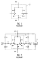
- a frequently used circuit configuration is a differential pair 10 of bipolar transistors, as shown in Fig. 1.
- this configuration is used as an input with the bases of the transistors connected to external bonding pads, it is very difficult to protect these transistors from ESD events.
- US-A-4206418 describes a circuit including means for limiting the potential difference that can exist between corresponding electrodes of two input transistors interconnected to form a differential amplifier stage.
- the control electrode of each input transistor is coupled via a normally conducting gating transistor to its respective input terminal and via a normally non-conducting clamping transistor to a common point to which is connected one end (source or emitter) of the main conduction paths of the two input transistors.
- the gating transistor is turned off and decouples the control electrode of the input transistor from its corresponding input terminal.
- the circuit may also include means connected to the output (drain or collector) electrodes of the two input transistor to prevent excessive voltage differentials between their output electrodes.
- WO92/07402 describes a circuit protection arrangement comprises a series switching circuit that is intended to be connected in a line of the circuit and will switch to an open state when subjected to an over current, and a shunt switching circuit that is open under normal operating conditions but will shunt the over current across the load of the circuit or to ground when triggered by the series switching circuit.
- the series switching circuit comprises a switching transistor (4) that is controlled by a control transistor (6)
- the shunt switching circuit comprises a shunt-switching transistor (9) that is controlled by a shunt control transistor (11), which is itself controlled by the series switching circuit.
- the shunt switching circuit may be connected to ground or it may be connected to a back-up load or voltage foldback device such as a triac.
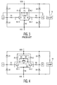
- FIG. 2 A typical ESD protection scheme is shown in Fig. 2. If pad A is stressed positive with respect to pad B, one of the likely paths for the ESD current is through a resistor R1, the forward biased base-emitter junction BE-1, the reverse biased base-emitter junction BE-2, and a resistor R2.
- transistors Q 1 and Q2 are small in area, significantly limiting the ability of the base-emitter junction to carry current in the forward direction before the internal power dissipation is sufficient to cause damage.
- the base-emitter junction is very weak in the reverse direction, with a typical breakdown voltage of 4 V or less.
- Resistors R1 and R2 are often low-valued resistors to improve performance. The result of this configuration is that it is very difficult to protect the differential pair against the effects of ESD events.
- the ESD protection scheme shown in FIG. 2 is required to limit the voltage between points C and D to a safe value during a typical ESD event, where the discharge current may exceed 2 A.
- the internal series resistance of the diode results in a larger forward drop (typically 2 to 3 V) than the typical low current diode drop (0.7 V).
- the preferred current path would be through diode D1, a power supply clamp 12, and diode D2. If it is assumed that the voltage drop across power supply clamp 12 is 5 V, and the voltage across each of the two diodes in forward bias under the ESD event is 3 V, then 11 V appears from pad A to pad B.
- An alternative approach is to divert the current from the input pads A and B directly.
- One such approach is shown in FIG. 3, where anti-parallel diodes, D5 and D6, are connected between pads A and B.
- This approach limits the voltage across the differential pair to one high current diode drop (approximately 3 V), if the same assumptions as in the above for FIG. 2 are used.
- the other diodes are also necessary to provide protection for ESD stresses from the pads to the power supply and ground.
- the major difficulty with this approach is that the input signal is also diverted by the diode pair D5 and D6, limiting the input swing to approximately 0.6 V in either polarity. If the input swing is larger than this voltage, the anti-parallel diodes D5 and D6 are no longer a valid solution for ESD protection.
- the invention provides a way of protecting a differential pair of bipolar transistors by diverting the current into an n-channel MOSFET which is driven into conduction during an ESD event and allows a larger swing of input voltage than the anti-parallel diode pair. No extra processing steps are required and the MOSFET is driven on, rather than relying on the parasitic bipolar npn transistor triggering into snap-back as in the grounded gate n-MOS transistor that is commonly used for ESD protection in CMOS integrated circuits.
- an ESD protection circuit for protecting a differential pair of transistors having two input terminals.
- the circuit comprises a switching element (such as an NMOS transistor) having first and second terminals and a control terminal; a first resistive element, coupled between the first and control terminals of the switching element; and a second resistive element, coupled between the second and control terminals of the switching element; wherein the first and second terminals of the switching element are for connecting, respectively, to input terminals of the different pair.
- the first and second resistive elements in the protection circuit are two resistors.
- the resistance values of the two resistors are preferably equal.
- each of the first and second resistive elements in the protection circuit includes a parallel circuit.
- Each parallel circuit includes a pair of anti-parallel diodes.
- each parallel circuit in the protection circuit further includes two resistors each connected in series with one of the diodes of the parallel circuit.
- the resistance values of the two resistors in each parallel circuit are preferably equal.
- FIG. 4 shows an ESD protection circuit 20 having a MOS transistor Q3 and resistors RC and RD.
- Transistor Q3 is placed with its source and drain directly in parallel with differential pair Q1 and Q2, between points C and D.
- transistor Q3 is a symmetrical NMOSFET designed using ESD rules (e.g., silicide is blocked on both sides of the gate to improve the reliability of the transistor under ESD stress).
- resistors RC and RD are equal in magnitude and large in value (typically 50k ⁇ to 100k ⁇ to limit the current through these resistors during normal operation.
- the time constant of the parallel combination of RC and RD and the gate to source capacitance of Q3 should typically be less than 1 nanosecond to assure that Q3 turns on fast enough to protect the bipolar transistors.
- the width of Q3 is determined by how much of the ESD event is to be absorbed in the structure, as discussed below.
- the length of Q3 may be the minimum value allowed in the process.
- the triggering voltage of the protection scheme using Q3 is determined by the threshold voltage, VT, of Q3 (typically 0.6 V). When the voltage from C to D reaches approximately twice the magnitude of VT in either polarity, Q3 will turn on to draw current. A voltage drop across resistors R1 and R2 will occur due to the current.
- the result will be that the pad voltage from A to B will continue to rise until the diode-clamp combination (D1, Clamp 12 and D4) becomes the primary current path, and the voltage across C to D remains clamped to approximately_twice VT.
- the size of resistors R1 and R2 determines the current level that Q3 must be able to absorb during an ESD event. In general, the larger R1 and R2, the smaller the width required for Q3, and vice versa. For example, if R1 and R2 are 1 ⁇ , and clamp 12 requires 5 V to trigger, then the current through R1 and R2 (and Q3) must be approximately 3 A before some of the current will be diverted from Q3.
- Fig. 5 illustrates an ESD protection circuit 20, in which resistors RC and RD are replaced with two pairs of anti-parallel diodes. This will provide a similar performance as that in Fig. 4, with a voltage swing limit of approximately 1.4 V.
- the present invention may also be used in place of the diode D 1 between pad A and power supply and the diode D2 between pad A and ground, and in a similar manner, in place of diodes D3 and D4 connected to pad B.
- the entire ESD event must go through the MOSFET, so the width of the device would be similar to that of the grounded gate MOSFET currently used as the primary protection in many CMOS integrated circuits.
Landscapes
- Semiconductor Integrated Circuits (AREA)
- Metal-Oxide And Bipolar Metal-Oxide Semiconductor Integrated Circuits (AREA)
- Emergency Protection Circuit Devices (AREA)
- Amplifiers (AREA)
- Control Of Eletrric Generators (AREA)
Claims (7)
- ESD-Schutzschaltung (20) zum Schützen eines Differential-Paares von Transistoren (Q1, Q2), das zwei Eingangsanschlüsse (A, B) aufweist,- mit einem Schaltelement (Q3), das erste und zweite Anschlüsse und einen Steueranschluss aufweist,- mit einem ersten Widerstandselement (RC), das zwischen dem ersten Anschluss und dem Steueranschluss des Schaltelementes geschaltet ist, und- mit einem zweiten Widerstandselement (RD), das zwischen dem zweiten Anschluss und dem Steueranschluss des Schaltelementes geschaltet ist,- wobei der erste und zweite Anschluss des Schaltelementes zum Verbinden mit entsprechenden Eingangsanschlüssen des Differential-Paares vorgesehen sind,dadurch gekennzeichnet, dass in der ESD-Schutzschaltung jedes der ersten und zweiten Widerstandselemente ein Paar antiparallel geschalteter Dioden enthält.
- Schaltung nach Anspruch 1, dadurch gekennzeichnet, dass das Schaltelement ein NMOS-Transistor und der Steueranschluss sein Gate-Anschluss ist.
- Schaltung nach Anspruch 1, dadurch gekennzeichnet, dass die ersten und zweiten Widerstandselemente zwei Widerstände sind.
- Schaltung nach Anspruch 3, dadurch gekennzeichnet, dass die Widerstandswerte der beiden Widerstände gleich sind.
- Schaltung nach Anspruch 1, dadurch gekennzeichnet, dass jedes der ersten und zweiten Widerstandselemente zwei Widerstände (RG, RJ, RH, RK) enthält, von denen jeder in Serie mit einer der Dioden der Parallelschaltung geschaltet ist.
- Schaltung nach Anspruch 5, dadurch gekennzeichnet, dass die Widerstandswerte der beiden Widerstände (RG, RJ, RH, RK) in jeder Parallelschaltung gleich sind.
- Schaltungsanordnung- mit einem Differential-Paar von Transistoren (Q1, Q2), das zwei Eingangsanschlüsse aufweist, und- mit einer ESD-Schutzschaltung (20) nach den vorhergehenden Ansprüchen, die zwischen die beiden Eingangsanschlüsse des Differential-Paares geschaltet ist.
Applications Claiming Priority (3)
| Application Number | Priority Date | Filing Date | Title |
|---|---|---|---|
| US733518 | 2000-12-07 | ||
| US09/733,518 US6507471B2 (en) | 2000-12-07 | 2000-12-07 | ESD protection devices |
| PCT/EP2001/013744 WO2002047166A2 (en) | 2000-12-07 | 2001-11-23 | Esd protection devices |
Publications (2)
| Publication Number | Publication Date |
|---|---|
| EP1356524A2 EP1356524A2 (de) | 2003-10-29 |
| EP1356524B1 true EP1356524B1 (de) | 2007-08-22 |
Family
ID=24947952
Family Applications (1)
| Application Number | Title | Priority Date | Filing Date |
|---|---|---|---|
| EP01991758A Expired - Lifetime EP1356524B1 (de) | 2000-12-07 | 2001-11-23 | Esd-schutzeinrichtungen |
Country Status (6)
| Country | Link |
|---|---|
| US (1) | US6507471B2 (de) |
| EP (1) | EP1356524B1 (de) |
| JP (1) | JP2004515923A (de) |
| AT (1) | ATE371268T1 (de) |
| DE (1) | DE60130146T2 (de) |
| WO (1) | WO2002047166A2 (de) |
Cited By (1)
| Publication number | Priority date | Publication date | Assignee | Title |
|---|---|---|---|---|
| TWI509928B (zh) * | 2013-03-15 | 2015-11-21 | Taiwan Semiconductor Mfg Co Ltd | 靜電放電防護裝置以及電路與解耦合方法 |
Families Citing this family (35)
| Publication number | Priority date | Publication date | Assignee | Title |
|---|---|---|---|---|
| US6650165B1 (en) * | 2002-05-02 | 2003-11-18 | Micrel, Incorporated | Localized electrostatic discharge protection for integrated circuit input/output pads |
| US6861711B2 (en) * | 2003-01-03 | 2005-03-01 | Micrel, Incorporated | Thick gate oxide transistor and electrostatic discharge protection utilizing thick gate oxide transistors |
| US6864537B1 (en) | 2003-01-03 | 2005-03-08 | Micrel, Incorporated | Thick gate oxide transistor and electrostatic discharge protection utilizing thick gate oxide transistors |
| US6888710B2 (en) | 2003-01-03 | 2005-05-03 | Micrel, Incorporated | Insulated gate bipolar transistor and electrostatic discharge cell protection utilizing insulated gate bipolar transistors |
| US6882224B1 (en) * | 2003-04-03 | 2005-04-19 | Xilinx, Inc. | Self-biasing for common gate amplifier |
| US7616414B2 (en) * | 2003-04-25 | 2009-11-10 | Broadcom Corporation | ESD protection circuit for high speed signaling including T/R switches |
| US6970337B2 (en) * | 2003-06-24 | 2005-11-29 | Linear X Systems Inc. | High-voltage low-distortion input protection current limiter |
| US7167331B1 (en) | 2003-10-23 | 2007-01-23 | Marvell International Ltd. | Electrostatic discharge protection circuit for magneto-resistive read elements |
| US7286328B1 (en) | 2003-10-23 | 2007-10-23 | Marvell International Ltd. | Electrostatic discharge protection circuit for preamps connected to magneto-resistive read elements |
| DE102004004789B3 (de) * | 2004-01-30 | 2005-03-03 | Infineon Technologies Ag | ESD-Schutzschaltkreis für eine elektronische Schaltung mit mehreren Versorgungsspannungen |
| US20050254158A1 (en) * | 2004-05-13 | 2005-11-17 | Kuehne Stephen C | ESD protection for differential mode magnetic transducer |
| JP3874776B2 (ja) * | 2004-10-15 | 2007-01-31 | ローム株式会社 | 演算増幅器 |
| DE102004052868B4 (de) * | 2004-11-02 | 2007-02-08 | Infineon Technologies Ag | Integrierte Schaltkreis-Anordnung und Schaltkreis-Array |
| US8144441B2 (en) * | 2006-08-30 | 2012-03-27 | Triquint Semiconductor, Inc. | Electrostatic discharge protection circuit for compound semiconductor devices and circuits |
| US7974053B2 (en) * | 2008-05-29 | 2011-07-05 | Amazing Microelectronic Corp | ESD protection circuit for differential I/O pair |
| US7826188B2 (en) * | 2008-06-17 | 2010-11-02 | International Business Machines Corporation | Methods, design structures, and systems for current mode logic (CML) differential driver ESD protection circuitry |
| US8823417B2 (en) * | 2008-07-09 | 2014-09-02 | Siemens Industry, Inc. | Combination AC/DC peak detector and signal type discriminator |
| US7880195B2 (en) * | 2008-12-08 | 2011-02-01 | United Microelectronics Corp. | Electrostatic discharge protection device and related circuit |
| US20110089902A1 (en) * | 2009-10-21 | 2011-04-21 | K2 Energy Solutions, Inc. | Circuitry for balancing charging of series connected battery cells |
| US8008970B1 (en) | 2010-06-07 | 2011-08-30 | Skyworks Solutions, Inc. | Apparatus and method for enabled switch detection |
| US8656761B2 (en) * | 2011-05-27 | 2014-02-25 | General Electric Company | Systems and methods for use in providing a sensor signal independent of ground |
| CN102957136B (zh) * | 2011-08-19 | 2015-01-14 | 登丰微电子股份有限公司 | 具有冲击电流保护的负载驱动电路 |
| WO2013106484A1 (en) * | 2012-01-09 | 2013-07-18 | Skyworks Solutions, Inc. | Devices and methods related to electrostatic discharge-protected cmos switches |
| EP2815478B1 (de) * | 2012-02-15 | 2017-03-22 | Qualcomm Incorporated | Überspannungsschutz für differentielle eingangs-/ausgangsschnittstellen |
| US9929698B2 (en) * | 2013-03-15 | 2018-03-27 | Qualcomm Incorporated | Radio frequency integrated circuit (RFIC) charged-device model (CDM) protection |
| US10026729B2 (en) * | 2014-03-12 | 2018-07-17 | Mediatek Inc. | Surge-protection circuit and surge-protection method |
| US9882377B2 (en) | 2015-01-28 | 2018-01-30 | International Business Machines Corporation | Electrostatic discharge protection solutions |
| TWI591795B (zh) | 2016-05-09 | 2017-07-11 | 瑞昱半導體股份有限公司 | 靜電放電保護電路 |
| CN107369672A (zh) * | 2016-05-12 | 2017-11-21 | 瑞昱半导体股份有限公司 | 静电放电保护电路 |
| TWI627809B (zh) * | 2017-01-25 | 2018-06-21 | 瑞昱半導體股份有限公司 | 靜電放電防護電路 |
| US10547312B2 (en) * | 2017-03-15 | 2020-01-28 | Silicon Laboratories Inc. | Wide voltage range input interface |
| TWI654733B (zh) * | 2018-06-04 | 2019-03-21 | 茂達電子股份有限公司 | 靜電放電保護電路 |
| CN110198028B (zh) * | 2019-05-13 | 2021-08-24 | 深圳市华星光电半导体显示技术有限公司 | 静电防护电路 |
| US11664741B2 (en) * | 2019-07-25 | 2023-05-30 | Susan Rhodes | System and method for AC power control |
| US11398468B2 (en) * | 2019-12-12 | 2022-07-26 | Micron Technology, Inc. | Apparatus with voltage protection mechanism |
Family Cites Families (9)
| Publication number | Priority date | Publication date | Assignee | Title |
|---|---|---|---|---|
| US3879640A (en) * | 1974-02-11 | 1975-04-22 | Rca Corp | Protective diode network for MOS devices |
| US4044313A (en) * | 1976-12-01 | 1977-08-23 | Rca Corporation | Protective network for an insulated-gate field-effect (IGFET) differential amplifier |
| US4206418A (en) * | 1978-07-03 | 1980-06-03 | Rca Corporation | Circuit for limiting voltage differential in differential amplifiers |
| JPS55154809A (en) * | 1979-05-23 | 1980-12-02 | Toshiba Corp | Input protecting circuit of operational amplifier |
| US4940907A (en) * | 1989-01-19 | 1990-07-10 | Ford Motor Company | Precision CMOS comparator with hysteresis |
| PT99196B (pt) * | 1990-10-12 | 1999-02-26 | Raychem Ltd | Dispositivo para a proteccao de circuitos e unidade de proteccao que os compreende |
| US5311083A (en) | 1993-01-25 | 1994-05-10 | Standard Microsystems Corporation | Very low voltage inter-chip CMOS logic signaling for large numbers of high-speed output lines each associated with large capacitive loads |
| US5574618A (en) * | 1994-02-17 | 1996-11-12 | Harris Corporation | ESD protection using SCR clamping |
| US5862031A (en) * | 1997-11-26 | 1999-01-19 | Analog Devices, Inc. | ESD protection circuit for integrated circuits having a bipolar differential input |
-
2000
- 2000-12-07 US US09/733,518 patent/US6507471B2/en not_active Expired - Fee Related
-
2001
- 2001-11-23 JP JP2002548786A patent/JP2004515923A/ja active Pending
- 2001-11-23 EP EP01991758A patent/EP1356524B1/de not_active Expired - Lifetime
- 2001-11-23 WO PCT/EP2001/013744 patent/WO2002047166A2/en not_active Ceased
- 2001-11-23 DE DE60130146T patent/DE60130146T2/de not_active Expired - Lifetime
- 2001-11-23 AT AT01991758T patent/ATE371268T1/de not_active IP Right Cessation
Cited By (1)
| Publication number | Priority date | Publication date | Assignee | Title |
|---|---|---|---|---|
| TWI509928B (zh) * | 2013-03-15 | 2015-11-21 | Taiwan Semiconductor Mfg Co Ltd | 靜電放電防護裝置以及電路與解耦合方法 |
Also Published As
| Publication number | Publication date |
|---|---|
| WO2002047166A2 (en) | 2002-06-13 |
| EP1356524A2 (de) | 2003-10-29 |
| US6507471B2 (en) | 2003-01-14 |
| WO2002047166A3 (en) | 2003-08-07 |
| US20020071230A1 (en) | 2002-06-13 |
| DE60130146T2 (de) | 2008-05-21 |
| ATE371268T1 (de) | 2007-09-15 |
| JP2004515923A (ja) | 2004-05-27 |
| DE60130146D1 (de) | 2007-10-04 |
Similar Documents
| Publication | Publication Date | Title |
|---|---|---|
| US6507471B2 (en) | ESD protection devices | |
| EP1417758B1 (de) | Esd-schutzvorrichtungen für ein differentielles transistorpaar | |
| US5946175A (en) | Secondary ESD/EOS protection circuit | |
| KR100297014B1 (ko) | Npn 바이폴라 트랜지스터를 사용하는 정전방전(esd)보호 | |
| US7400480B2 (en) | Electrostatic discharge protection circuit | |
| US6442008B1 (en) | Low leakage clamp for E.S.D. protection | |
| KR980006248A (ko) | 고전압 보호회로를 갖는 집적회로 | |
| KR100854008B1 (ko) | 정전기 방전으로부터 전기 엘리먼트를 보호하는 방법 및 장치 | |
| JPH11252780A (ja) | シュミットトリガ構成を有する電磁放電防止回路 | |
| EP0783787B1 (de) | Abschaltvorrichtung | |
| JP2549741B2 (ja) | Cmos集積回路用の静電放電気からの保護回路 | |
| US5644460A (en) | Multi-rail electrostatic discharge protection device | |
| JP2007511901A (ja) | アクティブ保護回路装置 | |
| US5535086A (en) | ESD protection circuit and method for BICMOS devices | |
| US5990723A (en) | Filter circuits for protecting against transient electrical pulses | |
| US20250248130A1 (en) | Electrostatic discharge clamp circuit containing a disable circuit to selectively disable a discharge circuit | |
| JPH11289053A (ja) | 静電気放電保護装置 | |
| US5745327A (en) | Device for preventing surge noise in connecting computers and peripherals thereof | |
| JP3003825B2 (ja) | サージ電圧保護回路 | |
| KR0154824B1 (ko) | 히스테리시스 특성을 갖는 전류제한 보호회로 | |
| WO2025165405A1 (en) | Electrostatic discharge clamp circuit containing a disable circuit to selectively disable a discharge circuit | |
| JPH0575031A (ja) | 半導体装置 | |
| JPH10500840A (ja) | 電流制限用回路装置 | |
| JPH05335567A (ja) | 半導体装置 | |
| JPH0471320A (ja) | 過電流防止回路 |
Legal Events
| Date | Code | Title | Description |
|---|---|---|---|
| PUAI | Public reference made under article 153(3) epc to a published international application that has entered the european phase |
Free format text: ORIGINAL CODE: 0009012 |
|
| AK | Designated contracting states |
Kind code of ref document: A2 Designated state(s): AT BE CH CY DE DK ES FI FR GB GR IE IT LI LU MC NL PT SE TR |
|
| 17P | Request for examination filed |
Effective date: 20040209 |
|
| GRAP | Despatch of communication of intention to grant a patent |
Free format text: ORIGINAL CODE: EPIDOSNIGR1 |
|
| RIC1 | Information provided on ipc code assigned before grant |
Ipc: H01L 27/02 20060101AFI20070213BHEP Ipc: H02H 9/04 20060101ALI20070213BHEP Ipc: H03K 17/0812 20060101ALI20070213BHEP |
|
| GRAS | Grant fee paid |
Free format text: ORIGINAL CODE: EPIDOSNIGR3 |
|
| GRAA | (expected) grant |
Free format text: ORIGINAL CODE: 0009210 |
|
| RAP1 | Party data changed (applicant data changed or rights of an application transferred) |
Owner name: NXP B.V. |
|
| AK | Designated contracting states |
Kind code of ref document: B1 Designated state(s): AT BE CH CY DE DK ES FI FR GB GR IE IT LI LU MC NL PT SE TR |
|
| REG | Reference to a national code |
Ref country code: GB Ref legal event code: FG4D |
|
| REG | Reference to a national code |
Ref country code: CH Ref legal event code: EP |
|
| REG | Reference to a national code |
Ref country code: IE Ref legal event code: FG4D |
|
| REF | Corresponds to: |
Ref document number: 60130146 Country of ref document: DE Date of ref document: 20071004 Kind code of ref document: P |
|
| ET | Fr: translation filed | ||
| PG25 | Lapsed in a contracting state [announced via postgrant information from national office to epo] |
Ref country code: ES Free format text: LAPSE BECAUSE OF FAILURE TO SUBMIT A TRANSLATION OF THE DESCRIPTION OR TO PAY THE FEE WITHIN THE PRESCRIBED TIME-LIMIT Effective date: 20071203 Ref country code: FI Free format text: LAPSE BECAUSE OF FAILURE TO SUBMIT A TRANSLATION OF THE DESCRIPTION OR TO PAY THE FEE WITHIN THE PRESCRIBED TIME-LIMIT Effective date: 20070822 Ref country code: NL Free format text: LAPSE BECAUSE OF FAILURE TO SUBMIT A TRANSLATION OF THE DESCRIPTION OR TO PAY THE FEE WITHIN THE PRESCRIBED TIME-LIMIT Effective date: 20070822 |
|
| NLV1 | Nl: lapsed or annulled due to failure to fulfill the requirements of art. 29p and 29m of the patents act | ||
| PG25 | Lapsed in a contracting state [announced via postgrant information from national office to epo] |
Ref country code: AT Free format text: LAPSE BECAUSE OF FAILURE TO SUBMIT A TRANSLATION OF THE DESCRIPTION OR TO PAY THE FEE WITHIN THE PRESCRIBED TIME-LIMIT Effective date: 20070822 Ref country code: LI Free format text: LAPSE BECAUSE OF FAILURE TO SUBMIT A TRANSLATION OF THE DESCRIPTION OR TO PAY THE FEE WITHIN THE PRESCRIBED TIME-LIMIT Effective date: 20070822 Ref country code: CH Free format text: LAPSE BECAUSE OF FAILURE TO SUBMIT A TRANSLATION OF THE DESCRIPTION OR TO PAY THE FEE WITHIN THE PRESCRIBED TIME-LIMIT Effective date: 20070822 |
|
| REG | Reference to a national code |
Ref country code: CH Ref legal event code: PL |
|
| PG25 | Lapsed in a contracting state [announced via postgrant information from national office to epo] |
Ref country code: BE Free format text: LAPSE BECAUSE OF FAILURE TO SUBMIT A TRANSLATION OF THE DESCRIPTION OR TO PAY THE FEE WITHIN THE PRESCRIBED TIME-LIMIT Effective date: 20070822 |
|
| PG25 | Lapsed in a contracting state [announced via postgrant information from national office to epo] |
Ref country code: DK Free format text: LAPSE BECAUSE OF FAILURE TO SUBMIT A TRANSLATION OF THE DESCRIPTION OR TO PAY THE FEE WITHIN THE PRESCRIBED TIME-LIMIT Effective date: 20070822 Ref country code: GR Free format text: LAPSE BECAUSE OF FAILURE TO SUBMIT A TRANSLATION OF THE DESCRIPTION OR TO PAY THE FEE WITHIN THE PRESCRIBED TIME-LIMIT Effective date: 20071123 |
|
| PG25 | Lapsed in a contracting state [announced via postgrant information from national office to epo] |
Ref country code: PT Free format text: LAPSE BECAUSE OF FAILURE TO SUBMIT A TRANSLATION OF THE DESCRIPTION OR TO PAY THE FEE WITHIN THE PRESCRIBED TIME-LIMIT Effective date: 20080122 |
|
| PLBE | No opposition filed within time limit |
Free format text: ORIGINAL CODE: 0009261 |
|
| STAA | Information on the status of an ep patent application or granted ep patent |
Free format text: STATUS: NO OPPOSITION FILED WITHIN TIME LIMIT |
|
| PG25 | Lapsed in a contracting state [announced via postgrant information from national office to epo] |
Ref country code: MC Free format text: LAPSE BECAUSE OF NON-PAYMENT OF DUE FEES Effective date: 20071130 Ref country code: SE Free format text: LAPSE BECAUSE OF FAILURE TO SUBMIT A TRANSLATION OF THE DESCRIPTION OR TO PAY THE FEE WITHIN THE PRESCRIBED TIME-LIMIT Effective date: 20071122 |
|
| 26N | No opposition filed |
Effective date: 20080526 |
|
| PG25 | Lapsed in a contracting state [announced via postgrant information from national office to epo] |
Ref country code: IE Free format text: LAPSE BECAUSE OF NON-PAYMENT OF DUE FEES Effective date: 20071123 |
|
| PG25 | Lapsed in a contracting state [announced via postgrant information from national office to epo] |
Ref country code: CY Free format text: LAPSE BECAUSE OF FAILURE TO SUBMIT A TRANSLATION OF THE DESCRIPTION OR TO PAY THE FEE WITHIN THE PRESCRIBED TIME-LIMIT Effective date: 20070822 |
|
| PG25 | Lapsed in a contracting state [announced via postgrant information from national office to epo] |
Ref country code: LU Free format text: LAPSE BECAUSE OF NON-PAYMENT OF DUE FEES Effective date: 20071123 |
|
| PG25 | Lapsed in a contracting state [announced via postgrant information from national office to epo] |
Ref country code: TR Free format text: LAPSE BECAUSE OF FAILURE TO SUBMIT A TRANSLATION OF THE DESCRIPTION OR TO PAY THE FEE WITHIN THE PRESCRIBED TIME-LIMIT Effective date: 20070822 |
|
| PGFP | Annual fee paid to national office [announced via postgrant information from national office to epo] |
Ref country code: DE Payment date: 20091119 Year of fee payment: 9 |
|
| PGFP | Annual fee paid to national office [announced via postgrant information from national office to epo] |
Ref country code: FR Payment date: 20091123 Year of fee payment: 9 Ref country code: GB Payment date: 20091118 Year of fee payment: 9 |
|
| PG25 | Lapsed in a contracting state [announced via postgrant information from national office to epo] |
Ref country code: IT Free format text: LAPSE BECAUSE OF NON-PAYMENT OF DUE FEES Effective date: 20071130 |
|
| GBPC | Gb: european patent ceased through non-payment of renewal fee |
Effective date: 20101123 |
|
| REG | Reference to a national code |
Ref country code: FR Ref legal event code: ST Effective date: 20110801 |
|
| REG | Reference to a national code |
Ref country code: DE Ref legal event code: R119 Ref document number: 60130146 Country of ref document: DE Effective date: 20110601 Ref country code: DE Ref legal event code: R119 Ref document number: 60130146 Country of ref document: DE Effective date: 20110531 |
|
| PG25 | Lapsed in a contracting state [announced via postgrant information from national office to epo] |
Ref country code: FR Free format text: LAPSE BECAUSE OF NON-PAYMENT OF DUE FEES Effective date: 20101130 |
|
| PG25 | Lapsed in a contracting state [announced via postgrant information from national office to epo] |
Ref country code: GB Free format text: LAPSE BECAUSE OF NON-PAYMENT OF DUE FEES Effective date: 20101123 |
|
| PG25 | Lapsed in a contracting state [announced via postgrant information from national office to epo] |
Ref country code: DE Free format text: LAPSE BECAUSE OF NON-PAYMENT OF DUE FEES Effective date: 20110531 |