EP1357779A1 - Dispositif haute frequence - Google Patents
Dispositif haute frequence Download PDFInfo
- Publication number
- EP1357779A1 EP1357779A1 EP02800730A EP02800730A EP1357779A1 EP 1357779 A1 EP1357779 A1 EP 1357779A1 EP 02800730 A EP02800730 A EP 02800730A EP 02800730 A EP02800730 A EP 02800730A EP 1357779 A1 EP1357779 A1 EP 1357779A1
- Authority
- EP
- European Patent Office
- Prior art keywords
- board
- frequency
- frequency device
- output
- frame
- Prior art date
- Legal status (The legal status is an assumption and is not a legal conclusion. Google has not performed a legal analysis and makes no representation as to the accuracy of the status listed.)
- Withdrawn
Links
Images


Classifications
-
- H—ELECTRICITY
- H05—ELECTRIC TECHNIQUES NOT OTHERWISE PROVIDED FOR
- H05K—PRINTED CIRCUITS; CASINGS OR CONSTRUCTIONAL DETAILS OF ELECTRIC APPARATUS; MANUFACTURE OF ASSEMBLAGES OF ELECTRICAL COMPONENTS
- H05K9/00—Screening of apparatus or components against electric or magnetic fields
- H05K9/0007—Casings
- H05K9/006—Casings specially adapted for signal processing applications, e.g. CATV, tuner, antennas amplifier
Definitions
- the present invention relates to a high-frequency device including plural high-frequency circuits, in which the high-frequency circuits are prevented from leakage and radiation of undesired high-frequency signals between the circuits.
- a VHF/UHF tuner for receiving television (TV) signals as a conventional high-frequency device will be described.
- the VHF/UHF tuner includes a VHF section and a UHF section. Since the sections are almost the same in structure, the VHF section will be explained. As shown in Fig.
- the VHF section includes input terminal 1 for receiving the TV signals, low-pass filter (LPF) 2a coupled to input terminal 1, tuning filter 3a coupled to an output of LPF 2a, high-frequency amplifier 4a coupled to an output of tuning filter 3a, inter-stage filter 5a coupled to an output of high-frequency amplifier 4a, mixer 7a having an input port coupled to an output of inter-stage filter 5a and another input port coupled to an output of local oscillator 6a, intermediate-frequency amplifier 8 coupled to an output of mixer 7a, and output terminal 9 coupled to an output of intermediate-frequency amplifier 8.
- LPF low-pass filter
- the UHF section includes high-pass filter 2b instead of low-pass filter 2a in the VHF section. That is, filters 2a and 2b separates the received signals into VHF signals and UHF signals. Other than this are substantially identical to each other between the two sections except for handling frequencies of different bandwidths.
- components of the UHF section commonly used in the VHF section are denoted by reference numerals with a subscript "b".
- Input terminal 1, intermediate-frequency amplifier 8, and output terminal 9 are shared between the two sections.
- circuits are formed on a printed circuit board, and are accommodated, as shown in Fig. 8, in metallic shield case 10. To avoid interference between circuits, these circuits are isolated from each other by metallic partitions 11 in high frequencies.
- Partition 11a is located between tuning filters 3a, 3b and inter-stage filters 5a, 5b, and more specifically, located above transistors in high-frequency amplifiers 4a and 4b. If outputs from high-frequency amplifiers 4a and 4b return upstream, abnormal oscillation may occurs. Partition 11a is inserted to avoid the inconvenience.
- Partition 11b is located between local oscillators 6a, 6b and inter-stage filters 5a, 5b. Partition 11b blocks leakage of signals generated by local oscillators 6a and 6b through input terminal 1 to the outside, which may affects other televisions. For designing a device that uses public radio waves with others, it is important to avoid affecting others. The leakage of signals is thus double-blocked by partitions 11b and 11a.
- partitions 11a and 11b are made of metal, and isolates electrically and mechanically between the circuits.
- the circuits include components which are limited in their arrangement.
- a high-frequency device includes a board, plural high-frequency circuits provided on the board, and a partition located between the high-frequency circuits and including a frame made of conductive material.
- the frame prevents a signal generated in the high-frequency circuits from passing through said frame.
- the high-frequency device is not limited in arrangement of components.
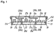
- Fig. 1 is a sectional view of a high-frequency device according to an exemplary embodiment of the present invention.
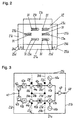
- Fig. 2 shows an exploded view of a shield case of the high-frequency device.
- metallic shield case 20 has bottom 22 and sides 21a, 21b, 21c, and 21d formed by Bending each side of a rectangular plate. Bent-up strips 23a, 23b, 23c, 23d, 23e, and 23f are formed on bottom 22 by bending up a portion of - the bottom.
- Legs 24b and 24d are formed unitarily with sides 21b and 21d, respectively.
- insert portions 25b and 25d are formed with legs 24b and 24d, respectively. Insert portions 25b and 25d are inserted into a printed circuit board for having high-frequency components mounted thereon, and are soldered with the circuit board.
- single-sided printed circuit board 26 having a high-frequency circuit mounted thereon is accommodated in shield case 20.
- high-frequency electronic components 27 including core-less coils 27a, 27b, and chip component 27c are mounted by reflow soldering.
- Printed circuit board 26 has holes 28a and 28d into which bent-up strips 23a and 23d are inserted then soldered, respectively. Bent-up strips 23a and 23d have holders 31 at their bases, as shown in Fig. 2. Holder 31 supports printed circuit board 26. Printed circuit board 26 is held and secured mainly by lug 30 located on side 21 of shield case 20.
- Metallic lid 32 for covering shield case 20 has contact lugs 33a to 33f corresponding to bent-up strips 23a-23f of case 20.
- Contact lugs 33a to 33f is elastic since being formed by bent up, so that the lugs elastically contacts strips 23a to 23f, respectively.
- bottom 22, bent-up strips 23a-23f, contact lugs 33a-33f, and lid 32 form frame 50 made of conductive material.
- Frame 50 has a side shorter than the wavelength of a signal generated in the high-frequency device mounted on the printed circuit board.
- the distances between strips 23a-23f for example, the distance between strip 23a and strip 23d should be shorter than the wavelength of the signal. This prevents the signal from passing through the frame.
- Frame 50 serves not only as a partition of the high-frequency circuits, but also as a protector against interference between the circuits.
- electronic components 27c and 27d can be located within frame 50.
- frame 50 is located between core-less coils 27a and 27b, and located between chip components 27c and 27d.
- Frame 50 of the embodiment has a rectangular shape, however, may have a round or oval shaped, providing the same effect.
- the round shape has a diameter shorter than the wavelength of an undesired signal, or the oval shape has a long-axis diameter shorter than the wavelength for blocking the signal.
- Fig. 3 is a circuit diagram of a VHF/UHF tuner for receiving television (TV) signals as the high-frequency device of the embodiment.
- the VHF/UHF tuner includes a VHF section and a UHF section.
- the VHF section includes input terminal 41 for receiving TV signals, low-pass filter (LPF) 42a coupled to input terminal 41, tuning filter 43a coupled to an output of LPF 42a, high-frequency amplifier 44a coupled to an output of tuning filter 43a, inter-stage filter 45a coupled to an output of high-frequency amplifier 44a, mixer 47a having an input port coupled to an output of inter-stage filter 45a and another input port coupled to an output of local oscillator 46a, intermediate frequency amplifier 48 coupled to an output of mixer 47a, and output terminal 49 coupled to an output of intermediate frequency amplifier 48.
- LPF low-pass filter
- the UHF section includes high-pass filter (HPF) 42b instead of LPF 42a in the VHF section. That is, filters 42a and 42b separate signals into VHF signals and UHF signals. Other portions of the two sections are substantially the same except handling frequencies of different bandwidths.
- HPF high-pass filter
- Input terminal 41, intermediate frequency amplifier 48, and output terminal 49 are shared between the two sections.
- the VHF/UHF tuner having the structure above will be described. As described above, operations of the sections except their handling frequencies of different bandwidths are almost identical. Therefore, the VHF section will be mainly explained.
- a VHF signal out of TV signals received at input terminal is supplied to tuning filter 43a through LPF 42a.
- a UHF signal out of the TV signals is supplied to tuning filter 43b through HPF 42b. That is, filters 42a and 42b separate the input signals into the VHF signal and the UHF signal.
- the VHF signal will be mainly explained.
- Tuning filter 43a has a variable center frequency, which allows frequencies near a desired center frequency to pass through the filter.
- An output of tuning filter 43a is supplied to inter-stage filter 45a via high-frequency amplifier 44a including a transistor.
- Frame 50a formed of bent-up strips 23b, 23f, bottom 22, and lid 32 is located between an input section and an output section of amplifier 44a for preventing an output of high-frequency amplifier 44a from returning back upstream.
- Frame 50a has a side shorter than the wavelength of a frequency passing through amplifier 44a. Frame 50a having such structure therefore blocks the output from returning back to input terminal 41, and thus prevents the circuit from abnormal oscillation.
- Inter-stage filter 45a has a sharp cut-off profile and a passing band narrower than tuning filter 43a, thus allowing only a desired frequency to pass through the filter.
- An output of the filter is supplied to one input port of mixer 47a for mixing the output with an output of local oscillator 46a received at another input port of mixer 47a.
- Mixer 47a outputs an intermediate frequency signal.
- Frames 50b and 50c are located between local oscillator 46a, mixer 47a and inter-stage filter 45a to prevent leakage of a signal from local oscillator 46a to input terminal 41.
- Frame 50b is formed of side 21c, bent-up strip 23c, bottom 22, and lid 32.
- frame 50c is formed of bent-up strips 23c and 23e, bottom 22, and lid 32.
- the output of local oscillator 46a has to pass through frame 50b, or frames 50a and 50c to reach input terminal 41.
- Frames 50b and 50c have sides shorter than the wavelength of the output of local oscillator 46a.
- Frames 50b and 50c having such structures can function as a barrier against the output of local oscillator 46a. That is, frames 50b and 50c can double-block the output of oscillator 46a from reaching input terminal 41.
- mixer 47a The output of mixer 47a is amplified by intermediate frequency amplifier 48 and is then brought to output terminal 49.
- the UHF section includes frame 50d located between an input port and an output port of high-frequency amplifier 44b to preventing an output of amplifier 44b from returning back to input terminal 41.
- Frame 50d is formed of bent-up strips 23a and 23b, bottom 22, and lid 32.
- Frame 50d has a side shorter than the wavelength of a frequency passing through amplifier 44b. Frame 50d having such structure therefore prevents the output from returning back to input terminal 41, thus protecting the circuit from abnormal oscillation.
- Inter-stage filter 45b has a sharp cut-off profile and a passing band narrower than tuning filter 43b, thus allowing only a desired frequency to pass through.
- the output is supplied to one input port of mixer 47b for mixing the output with an output of local oscillator 46b received at another input port of mixer 47a.
- Mixer 47b outputs an intermediate frequency signal.
- Frames 50e and 50f are located between local oscillator 46b, mixer 47b and inter-stage filter 45b in order to protect leakage of a signal from local oscillator 46b to input terminal 41.
- Frame 50e is formed of side 21a, bent-up strip 23d, bottom 22, and lid 32.
- frame 50f is formed of bent-up strips 23d and 23e, bottom 22, and lid 32.
- the oscillated output signal of local oscillator 46b has to pass through frame 50e, or frames 50f and 50d to reach input terminal 41.
- Frames 50e and 50f have sides shorter than the wavelength of the output of local oscillator 46b. That is, frames 50e and 50f can prevent the output of oscillator 46b from reaching input terminal 41.
- Core-less coil 51 forms tuning filter 43
- core-less coil 52 forms inter-stage filter 45
- Frame 50 formed of bent-up strip 23, bottom 22, and lid 32 is located between core-less coils 51 and 52.
- Frame 50 reduces electromagnetic coupling between core-less coils 51 and 52, thus preventing interference between the coils.
- core-less coils 51 and 52 are located so that respective center axes of the coils are substantially perpendicular (angle 53) to each other, as shown in Fig. 4. This arrangement reduces the coupling between core-less coils 51 and 52, thus preventing the coils from interference.
- Fig. 5 shows an arrangement of core-less coils 54 and 55 having respective center axes parallel to each other.
- Frame 50 formed of bent-up strip 23, bottom 22, and lid 32 is located between core-less coils 54 and 55, suppressing electromagnetic interference between the coils.
- an opening angle 57 not narrower than 45° is provided from center axis 56 of core-less coil 54, and core-less coil 55 is located out of the opening angle. This arrangement reduces the coupling between core-less coils 54 and 55, thus preventing the coils from interference.
- Fig. 6 is a plan view of a vicinity of a frame located between high-frequency circuits of the VHF/UHF tuner of the embodiment.
- Power supply pattern 60 is located adjacent to bent-up strip 23 penetrating the printed circuit board.
- Chip capacitor 62 is mounted between power supply pattern 60 and land 61 formed around bent-up strip 23.
- Chip capacitor 62 having a capacitance greater than 1000pF is connected directly to a ground (i.e., bent-up strip 23) can prevents interference waves through power supply pattern 60.
- Power supply pattern 60 being grounded via chip capacitor 62 reduces an impedance of pattern 60, thus protecting the circuit from undesired interference and electromagnetic coupling.
- the VHF/UHF tuner having such structure is accommodated in shield case 20, as shown in Figs. 1 and 2.
- the tuner does not require partitions 11a and 11b included in the conventional tuner.
- This structure can simplifies an arrangement of components, thereby contributing to a small, compact tuner. Furthermore, the structure allows the components of the tuner to be repaired and adjusted easily.
- the shield case can have side 21 by bending bottom 22, thus not needing a back lid.
- This structure simplifies not only the structure of the frame but also handling of the components.
- a single-sided printed circuit board has the components on its top surface, and does not have the components on bottom surface. Therefore, a shield case having the side formed by bending the bottom allows the components to be repaired and adjusted easily.
- a single-sided printed circuit board can also reduce the manufacturing cost of the device.
- the high-frequency device of the embodiment reduces a limitation in an arrangement of the components which increases board density, thus having a reduced size.
- the process of mounting component 27 on printed circuit board 26, and the process of fixing board 26 to shield case 20 can be simultaneously performed by reflow soldering.
- the strip formed by bending up the case itself serves as a side of the frame according to the embodiment.
- a rod-like, or plate-like piece instead of the bent-up strip may provides the same effect.
- the aforementioned piece is prepared separately from the case, and is then connected with the case.
- a conductive material-made frame serves as a partition between high-frequency electronic circuits.
- the frame has sides shorter than the wavelength of an undesired signal.
- the frame prevents leakage or radiation of undesired high frequencies.
- the high-frequency device employing the frame reduces limitation in an arrangement of the components mounted on a printed circuit board. This fact improves board density, thereby reducing the size of the device.
Landscapes
- Engineering & Computer Science (AREA)
- Signal Processing (AREA)
- Microelectronics & Electronic Packaging (AREA)
- Shielding Devices Or Components To Electric Or Magnetic Fields (AREA)
- Structure Of Receivers (AREA)
Applications Claiming Priority (3)
| Application Number | Priority Date | Filing Date | Title |
|---|---|---|---|
| JP2001307257 | 2001-10-03 | ||
| JP2001307257A JP3601497B2 (ja) | 2001-10-03 | 2001-10-03 | 高周波装置 |
| PCT/JP2002/010261 WO2003032703A1 (fr) | 2001-10-03 | 2002-10-02 | Dispositif haute frequence |
Publications (2)
| Publication Number | Publication Date |
|---|---|
| EP1357779A1 true EP1357779A1 (fr) | 2003-10-29 |
| EP1357779A4 EP1357779A4 (fr) | 2009-03-18 |
Family
ID=19126752
Family Applications (1)
| Application Number | Title | Priority Date | Filing Date |
|---|---|---|---|
| EP02800730A Withdrawn EP1357779A4 (fr) | 2001-10-03 | 2002-10-02 | Dispositif haute frequence |
Country Status (5)
| Country | Link |
|---|---|
| US (1) | US7046982B2 (fr) |
| EP (1) | EP1357779A4 (fr) |
| JP (1) | JP3601497B2 (fr) |
| CN (1) | CN1256860C (fr) |
| WO (1) | WO2003032703A1 (fr) |
Cited By (3)
| Publication number | Priority date | Publication date | Assignee | Title |
|---|---|---|---|---|
| EP1515598A1 (fr) * | 2003-09-12 | 2005-03-16 | Sony Ericsson Mobile Communications AB | Blindage pour une plaque de circuit et sa fabrication |
| WO2005027610A3 (fr) * | 2003-09-12 | 2005-06-23 | Sony Ericsson Mobile Comm Ab | Blindage pour carte de circuits imprimes et procede de fabrication associe |
| GB2428137A (en) * | 2005-07-07 | 2007-01-17 | Agilent Technologies Inc | Circuit board housing |
Families Citing this family (6)
| Publication number | Priority date | Publication date | Assignee | Title |
|---|---|---|---|---|
| US7145783B2 (en) * | 2004-06-07 | 2006-12-05 | Ford Global Technologies, Llc | Apparatus reducing radiated emission from electronic modules |
| US7183500B2 (en) * | 2004-06-30 | 2007-02-27 | Intel Corporation | Electromagnetic interference (EMI) filter with passive noise cancellation |
| US7728417B2 (en) * | 2005-05-27 | 2010-06-01 | Stats Chippac Ltd. | Integrated circuit package system including shield |
| WO2009060337A2 (fr) * | 2007-11-05 | 2009-05-14 | Nxp B.V. | Architecture de mélangeur |
| FR2984462A1 (fr) * | 2011-12-15 | 2013-06-21 | Valeo Vision | Dispositif d'eclairage et/ou de signalisation et vehicule automobile comprenant un tel dispositif. |
| CN111373664B (zh) * | 2017-11-28 | 2022-07-29 | 索尼半导体解决方案公司 | 调谐器模块和接收装置 |
Family Cites Families (14)
| Publication number | Priority date | Publication date | Assignee | Title |
|---|---|---|---|---|
| DE2932015C2 (de) * | 1978-08-07 | 1983-12-29 | Mitsumi Electric Co., Ltd., Tokyo | Abschirmvorrichtung für Hochfrequenzschaltungen |
| JPS57173400A (en) | 1981-04-15 | 1982-10-25 | Toshiba Corp | Exciter for synchronous machine |
| JPS6244558Y2 (fr) * | 1981-04-24 | 1987-11-25 | ||
| FR2529430B1 (fr) | 1982-06-25 | 1985-08-09 | Telecommunications Sa | Structure de blindage pour circuit electrique, par exemple hyperfrequence, son procede de montage et l'outillage permettant de mettre en oeuvre ladite structure |
| CA1218713A (fr) * | 1983-05-31 | 1987-03-03 | Hiroshi Saka | Circuit integre a micro-ondes insensible aux affets adverses du blindage |
| JPH0458596A (ja) * | 1990-06-28 | 1992-02-25 | Nippon Telegr & Teleph Corp <Ntt> | 電磁シールド方法 |
| JPH04117801A (ja) * | 1990-09-07 | 1992-04-17 | Mitsubishi Electric Corp | パッケージ |
| JPH0685501A (ja) * | 1992-09-04 | 1994-03-25 | Mitsubishi Electric Corp | マイクロ波回路 |
| JPH1084194A (ja) * | 1996-09-09 | 1998-03-31 | Mitsubishi Electric Corp | 携帯端末のシールド構造 |
| JPH1131891A (ja) | 1997-07-11 | 1999-02-02 | Canon Inc | プリント基板の保持方法および保持構造 |
| JP3612959B2 (ja) * | 1997-11-11 | 2005-01-26 | 松下電器産業株式会社 | フィルタと、このフィルタを用いた高周波装置 |
| US6121546A (en) | 1998-04-20 | 2000-09-19 | Lucent Technologies Inc. | RF shield |
| JP2000032360A (ja) * | 1998-07-10 | 2000-01-28 | Matsushita Electric Ind Co Ltd | 高周波装置 |
| JP3691276B2 (ja) | 1999-02-22 | 2005-09-07 | シャープ株式会社 | 電子機器用筐体 |
-
2001
- 2001-10-03 JP JP2001307257A patent/JP3601497B2/ja not_active Expired - Fee Related
-
2002
- 2002-10-02 EP EP02800730A patent/EP1357779A4/fr not_active Withdrawn
- 2002-10-02 US US10/450,082 patent/US7046982B2/en not_active Expired - Fee Related
- 2002-10-02 CN CN02803391.4A patent/CN1256860C/zh not_active Expired - Fee Related
- 2002-10-02 WO PCT/JP2002/010261 patent/WO2003032703A1/fr not_active Ceased
Cited By (4)
| Publication number | Priority date | Publication date | Assignee | Title |
|---|---|---|---|---|
| EP1515598A1 (fr) * | 2003-09-12 | 2005-03-16 | Sony Ericsson Mobile Communications AB | Blindage pour une plaque de circuit et sa fabrication |
| WO2005027610A3 (fr) * | 2003-09-12 | 2005-06-23 | Sony Ericsson Mobile Comm Ab | Blindage pour carte de circuits imprimes et procede de fabrication associe |
| GB2428137A (en) * | 2005-07-07 | 2007-01-17 | Agilent Technologies Inc | Circuit board housing |
| US7293999B2 (en) | 2005-07-07 | 2007-11-13 | Avago Technologies General Ip (Singapore) Pte. Ltd. | Housing of circuit boards |
Also Published As
| Publication number | Publication date |
|---|---|
| JP2003115687A (ja) | 2003-04-18 |
| US7046982B2 (en) | 2006-05-16 |
| US20040077329A1 (en) | 2004-04-22 |
| WO2003032703A1 (fr) | 2003-04-17 |
| CN1256860C (zh) | 2006-05-17 |
| CN1483304A (zh) | 2004-03-17 |
| JP3601497B2 (ja) | 2004-12-15 |
| EP1357779A4 (fr) | 2009-03-18 |
Similar Documents
| Publication | Publication Date | Title |
|---|---|---|
| KR100313590B1 (ko) | 튜너의구조체및이를사용한케이블모뎀튜너 | |
| US5668701A (en) | Up-down tuner having a grounding plate provided with generally L-shaped soldering portions | |
| US7046982B2 (en) | High frequency device having a frame with segmented compartments for prevented unwanted signal propagation | |
| JPH11122133A (ja) | テレビジョンチュ−ナ | |
| CN102696285A (zh) | 调谐器模块和接收设备 | |
| JP2002353842A (ja) | 携帯端末用無線モジュール | |
| EP0019437B1 (fr) | Dispositif pour la suppression d'interférences de radiofréquence | |
| EP1411756B1 (fr) | Appareil de fréquences radio | |
| US20030021095A1 (en) | Receiving apparatus | |
| US7194245B2 (en) | High-frequency signal receiving apparatus | |
| JP3729708B2 (ja) | 電子機器 | |
| US7247053B2 (en) | High-frequency apparatus having high performance and capable of preventing entry of interfering wave into terminal | |
| US20120314385A1 (en) | Circuit board and electronic apparatus | |
| JP3610196B2 (ja) | ダブルコンバージョンチューナ | |
| US7359693B2 (en) | Enclosure and substrate structure for a tuner module | |
| JP3139080B2 (ja) | カード型電子チューナ | |
| JP6848274B2 (ja) | 表示装置 | |
| JP4611902B2 (ja) | ダイバーシティ受信用チューナ | |
| JP3094608B2 (ja) | カード型電子チューナ | |
| JPH0715361A (ja) | Dbsチューナ | |
| JP2005354147A (ja) | テレビジョンチューナ | |
| JP2000269678A (ja) | 高周波装置 | |
| JPH05122012A (ja) | カード型電子チユーナ | |
| JPH0435305A (ja) | 受信コンバータ | |
| JP2002135140A (ja) | 送受信機用フロントエンド |
Legal Events
| Date | Code | Title | Description |
|---|---|---|---|
| PUAI | Public reference made under article 153(3) epc to a published international application that has entered the european phase |
Free format text: ORIGINAL CODE: 0009012 |
|
| 17P | Request for examination filed |
Effective date: 20030623 |
|
| AK | Designated contracting states |
Kind code of ref document: A1 Designated state(s): AT BE BG CH CY CZ DE DK EE ES FI FR GB GR IE IT LI LU MC NL PT SE SK TR |
|
| RAP1 | Party data changed (applicant data changed or rights of an application transferred) |
Owner name: PANASONIC CORPORATION |
|
| A4 | Supplementary search report drawn up and despatched |
Effective date: 20090216 |
|
| 17Q | First examination report despatched |
Effective date: 20090526 |
|
| STAA | Information on the status of an ep patent application or granted ep patent |
Free format text: STATUS: THE APPLICATION IS DEEMED TO BE WITHDRAWN |
|
| 18D | Application deemed to be withdrawn |
Effective date: 20120503 |