EP1364231B1 - Selbstreinigendes optisches gerät für die euv-lithographie - Google Patents
Selbstreinigendes optisches gerät für die euv-lithographie Download PDFInfo
- Publication number
- EP1364231B1 EP1364231B1 EP01987139A EP01987139A EP1364231B1 EP 1364231 B1 EP1364231 B1 EP 1364231B1 EP 01987139 A EP01987139 A EP 01987139A EP 01987139 A EP01987139 A EP 01987139A EP 1364231 B1 EP1364231 B1 EP 1364231B1
- Authority
- EP
- European Patent Office
- Prior art keywords
- layer
- mirror
- capping
- metal
- euv
- Prior art date
- Legal status (The legal status is an assumption and is not a legal conclusion. Google has not performed a legal analysis and makes no representation as to the accuracy of the status listed.)
- Revoked
Links
Images

Classifications
-
- G—PHYSICS
- G02—OPTICS
- G02B—OPTICAL ELEMENTS, SYSTEMS OR APPARATUS
- G02B1/00—Optical elements characterised by the material of which they are made; Optical coatings for optical elements
-
- B—PERFORMING OPERATIONS; TRANSPORTING
- B08—CLEANING
- B08B—CLEANING IN GENERAL; PREVENTION OF FOULING IN GENERAL
- B08B17/00—Methods preventing fouling
- B08B17/02—Preventing deposition of fouling or of dust
-
- B—PERFORMING OPERATIONS; TRANSPORTING
- B82—NANOTECHNOLOGY
- B82Y—SPECIFIC USES OR APPLICATIONS OF NANOSTRUCTURES; MEASUREMENT OR ANALYSIS OF NANOSTRUCTURES; MANUFACTURE OR TREATMENT OF NANOSTRUCTURES
- B82Y10/00—Nanotechnology for information processing, storage or transmission, e.g. quantum computing or single electron logic
-
- B—PERFORMING OPERATIONS; TRANSPORTING
- B82—NANOTECHNOLOGY
- B82Y—SPECIFIC USES OR APPLICATIONS OF NANOSTRUCTURES; MEASUREMENT OR ANALYSIS OF NANOSTRUCTURES; MANUFACTURE OR TREATMENT OF NANOSTRUCTURES
- B82Y40/00—Manufacture or treatment of nanostructures
-
- G—PHYSICS
- G03—PHOTOGRAPHY; CINEMATOGRAPHY; ANALOGOUS TECHNIQUES USING WAVES OTHER THAN OPTICAL WAVES; ELECTROGRAPHY; HOLOGRAPHY
- G03F—PHOTOMECHANICAL PRODUCTION OF TEXTURED OR PATTERNED SURFACES, e.g. FOR PRINTING, FOR PROCESSING OF SEMICONDUCTOR DEVICES; MATERIALS THEREFOR; ORIGINALS THEREFOR; APPARATUS SPECIALLY ADAPTED THEREFOR
- G03F1/00—Originals for photomechanical production of textured or patterned surfaces, e.g., masks, photo-masks, reticles; Mask blanks or pellicles therefor; Containers specially adapted therefor; Preparation thereof
- G03F1/22—Masks or mask blanks for imaging by radiation of 100nm or shorter wavelength, e.g. X-ray masks, extreme ultraviolet [EUV] masks; Preparation thereof
- G03F1/24—Reflection masks; Preparation thereof
-
- G—PHYSICS
- G03—PHOTOGRAPHY; CINEMATOGRAPHY; ANALOGOUS TECHNIQUES USING WAVES OTHER THAN OPTICAL WAVES; ELECTROGRAPHY; HOLOGRAPHY
- G03F—PHOTOMECHANICAL PRODUCTION OF TEXTURED OR PATTERNED SURFACES, e.g. FOR PRINTING, FOR PROCESSING OF SEMICONDUCTOR DEVICES; MATERIALS THEREFOR; ORIGINALS THEREFOR; APPARATUS SPECIALLY ADAPTED THEREFOR
- G03F7/00—Photomechanical, e.g. photolithographic, production of textured or patterned surfaces, e.g. printing surfaces; Materials therefor, e.g. comprising photoresists; Apparatus specially adapted therefor
- G03F7/70—Microphotolithographic exposure; Apparatus therefor
- G03F7/708—Construction of apparatus, e.g. environment aspects, hygiene aspects or materials
-
- G—PHYSICS
- G21—NUCLEAR PHYSICS; NUCLEAR ENGINEERING
- G21K—HANDLING OF PARTICLES OR IONISING RADIATION NOT OTHERWISE PROVIDED FOR; IRRADIATION DEVICES; GAMMA RAY OR X-RAY MICROSCOPES
- G21K1/00—Arrangements for handling particles or ionising radiation, e.g. focusing or moderating
- G21K1/06—Arrangements for handling particles or ionising radiation, e.g. focusing or moderating using diffraction, refraction or reflection, e.g. monochromators
- G21K1/062—Devices having a multilayer structure
-
- G—PHYSICS
- G21—NUCLEAR PHYSICS; NUCLEAR ENGINEERING
- G21K—HANDLING OF PARTICLES OR IONISING RADIATION NOT OTHERWISE PROVIDED FOR; IRRADIATION DEVICES; GAMMA RAY OR X-RAY MICROSCOPES
- G21K2201/00—Arrangements for handling radiation or particles
- G21K2201/06—Arrangements for handling radiation or particles using diffractive, refractive or reflecting elements
- G21K2201/067—Construction details
Definitions
- This invention pertains generally to a surface or "capping" layer for optics used for lithographic applications, and particularly for extreme ultraviolet lithography.
- the capping layer is such that it also protects the surface from oxidation or oxidative degradation.
- Hydrocarbon molecules and water vapor are ubiquitous in the photolithographic apparatus (stepper) used for EUVL. They are present in the background environment of the stepper and can arise from oils used in vacuum pumps that maintain the required low pressure atmosphere within the stepper as well as from other organic materials within the stepper environment such as photoresist materials and cabling. Water is adsorbed on all surfaces and is very difficult to remove in spite of the use of rigorous vacuum baking techniques. EUV radiation is energetic enough to cause the decomposition of water molecules adsorbed on or proximate to a surface to produce hydrogen and reactive oxygen species that can attack, degrade, or otherwise contaminate optical surfaces. EUV-induced dissociation of organic materials can cause the surfaces of multi-layer Mo/Si optics and masks to become contaminated with carbon.
- a method that can be used for removing carbon contamination employs oxygen-containing molecules, such as H 2 O and O 2 which in the presence of energetic radiation can form reactive chemical species that can react with carbon contamination to form volatile carbon compounds, such as CO and CO 2 , that can be pumped away. While the oxidative treatment works to remove carbon contamination, once the carbon layer is removed from the surface of the Mo/Si multi-layer optic structure, the reactive oxygen species can oxidize the underlying terminating silicon surface layer, forming silicon oxides (generally SiO 2 ). Oxygen is a strong absorber of EUV thus, oxidation of the Si-terminated Mo/Si optic would cause irreversible degradation of the reflective ability of these optics, as shown in FIG. 1.
- U.S. Patent 5,958,605 to Montcalm et al. discloses an overcoat (or "capping") layer applied to the surface of a Mo/Si multilayer mirror structure that resists oxidation.
- an overcoat layer or "capping" layer applied to the surface of a Mo/Si multilayer mirror structure that resists oxidation.
- the overcoat layer does not act to prevent carbon contamination of the multilayer optic.
- the reflective optics and masks used for EUVL are based on a Mo/Si multi-layer structure with the topmost layer consisting of about 40 ⁇ of silicon.
- a thin (about 5-400 ⁇ and preferably 5-10 ⁇ ) metal capping layer is deposited on top of the terminating silicon layer.
- this binding layer be thin (about 1-3 ⁇ ) so as not to materially affect transmission of incident radiation.
- a small pressure (about 10 -8 to 10 -4 Torr) of one or more of the aforementioned reactant gas species in the environment of the capped multilayer optic, and irradiated by EUV, will generate reactive atomic species which, in turn, will react with and remove any carbon contaminants deposited on the optic surface.
- atomic hydrogen can also be used to remove carbon from surfaces as CH 4 for example.
- the metal comprising the capping layer provide a catalytic surface for the binding and dissociation of molecular hydrogen to form atomic hydrogen.
- the present invention is directed to the use of a metal surface or "capping" layer for multilayer mirror structures, and particularly Mo/Si multilayer mirrors that, in combination with gaseous reactants and incident radiation, and particularly extreme ultraviolet (EUV) radiation, provide for continuous cleaning of carbon deposits from the surface.
- a metal surface or "capping" layer for multilayer mirror structures, and particularly Mo/Si multilayer mirrors that, in combination with gaseous reactants and incident radiation, and particularly extreme ultraviolet (EUV) radiation, provide for continuous cleaning of carbon deposits from the surface.
- EUV extreme ultraviolet
- FIG.2 which is used to illustrate and exemplify the invention, shows a typical multilayer reflective mirror structure 200 used for EUV applications.
- multiple alternating layers of Mo 210 and Si 220 comprise the multilayer coating 230 that is deposited onto a substrate 250.
- This particular configuration is used only for purposes of illustration, other structures are possible, such as non-periodic stacks, multilayer stacks with other materials, or more than two materials.
- a metal surface or capping layer 260 that has a typical thickness of 5-400 ⁇ and preferably 5-10 ⁇ , is deposited onto the terminating Si layer 225.
- Layer 260 is comprised of a metal or metal alloy that is not only oxidation resistant but also can bind and catalyze the dissociation of gaseous reactants to produce species that can react with and gasify carbon deposits in the presence of EUV radiation.
- Layer 260 also possesses the ability to transmit at least 90%, and preferably greater than 98%, of the incident EUV radiation, i.e., radiation in the wavelength range of 3-15 nm, and particularly at about 13.4 nm.
- a 10 ⁇ Ru film will transmit at least about 98.5% of the incident radiation at a wavelength of 13.4 nm.
- the reactive oxygen species can react with any carbon coating present on the surface of the metal capping layer as indicated by curve 120 of FIG. 1.
- Gaseous oxidizing reactants can be provided by admitting a small partial pressure about 10 -8 to 10 -4 Torr) of either or all of these oxygen containing gases into the environment of the multilayer mirror.
- curve 100 shows that the reflectivity of a Mo/Si multilayer mirror can be reduced as much as 7 % by exposure to a hydrocarbon vapor in the presence of EUV radiation (about 0.3 mW/mm 2 ) for about 3 hours.
- curve 120 shows no change in reflectivity indicating that any carbon, produced by radiation induced decomposition of the hydrocarbon material deposited on the mirror surface, was immediately oxidized away.
- the oxidizing reactant was removed (3-5 hrs) and the reflectivity began to fall as a carbon deposit began to build up on the mirror surface.
- the oxidizing reactant was again introduced (> 5 hrs.) and reflectivity began to rise indicating oxidative removal of the deposited carbon.
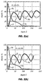
- FIGS. 3a and 3b show sputter Auger depth profile analysis of the interface between a 20 ⁇ thick Ru metal layer capping the Mo surface of a Mo/Si multilayer structure both before (3a) and after (3b) exposure to 5 x 10 -7 Torr water vapor for 4.5 hrs.
- the Ru capped Mo surface was irradiated with a flux of 2 kV electrons at a current density of 5 ⁇ A/cm 2 to simulate exposure to EUV radiation.
- EUV radiation interacts with the Mo/Si mirror and its capping layer to generate secondary electrons that provide for dissociation of reactant gas species
- an electron flux can be used to simulate easily and accurately the reactive conditions produced by EUV radiation.
- the Ru layer itself can also promote the dissociation of molecular H 2 O into reactive oxygen atoms.
- the Auger sputter profiles shown in FIGS. 3a and 3b are practically identical showing that both the Ru capping layer and the underlying terminating Mo surface of the multilayer mirror were not oxidized by the exposure conditions. Moreover, the EUV reflectivity (R) of the multilayer mirror remained practically unchanged, having a value of 63.0% before exposure and 62.8% after, a difference that is within measurement error.
- the metal capping layers can be applied by any means known to the art, such as by magnetron sputtering or e-beam evaporation. In some instances, particularly when the capping layer thickness is greater than about 100 ⁇ , it can be desirable to interpose a thin Cr, Mo, or Ti metal layer between the top surface of the multilayer mirror and the metal capping layer.
- the Cr, Mo, or Ti metal binding layer which can be about 1-3 ⁇ thick, can improve adherence of the capping layer.
- a surface such as the surface of an optic and particularly the surface of a multilayer mirror, with a metal capping layer that is both substantially transparent to radiation, and particularly to EUV radiation, and oxidation resistant, in combination with incident radiation and small amounts of a reactant gas such as H 2 O, O 2 or H 2 , which can be adventitiously present or added deliberately, it is possible to provide a surface which is not only resistant to oxidation but is also continuously cleaned of carbon deposits.
- a reactant gas such as H 2 O, O 2 or H 2
Landscapes
- Engineering & Computer Science (AREA)
- Physics & Mathematics (AREA)
- Nanotechnology (AREA)
- Chemical & Material Sciences (AREA)
- General Physics & Mathematics (AREA)
- Crystallography & Structural Chemistry (AREA)
- High Energy & Nuclear Physics (AREA)
- Epidemiology (AREA)
- Theoretical Computer Science (AREA)
- Manufacturing & Machinery (AREA)
- Spectroscopy & Molecular Physics (AREA)
- General Engineering & Computer Science (AREA)
- Mathematical Physics (AREA)
- Health & Medical Sciences (AREA)
- Environmental & Geological Engineering (AREA)
- Condensed Matter Physics & Semiconductors (AREA)
- Public Health (AREA)
- Optics & Photonics (AREA)
- Exposure Of Semiconductors, Excluding Electron Or Ion Beam Exposure (AREA)
- Exposure And Positioning Against Photoresist Photosensitive Materials (AREA)
- Optical Elements Other Than Lenses (AREA)
- Detergent Compositions (AREA)
- Organic Low-Molecular-Weight Compounds And Preparation Thereof (AREA)
- Cleaning In General (AREA)
Claims (13)
- Ein System für die extreme ultraviolette (EUV) Lithographie einschließend ein selbstreinigendes reflektierendes optisches Element aufweisend eine Basisoptik, welche einen Spiegel umfasst und eine Metalldeckschicht, welche auf einer EUV-reflektierenden Oberfläche des Spiegels angeordnet ist und welche die reflektierende Oberfläche gegen Oxidation schützt und mehr als 90 % der einfallenden EUV Strahlung auf die reflektierende Oberfläche leitet, dadurch gekennzeichnet, dass die metallische Deckschicht eine Rutheniumschicht ist.
- Lithographiesystem nach Anspruch 1, dadurch gekennzeichnet, dass der Spiegel ein Mehrschichtspiegel ist.
- Lithographiesystem nach Anspruch 1 oder 2, dadurch gekennzeichnet, dass der Spiegel eine Mehrzahl von Schichten aufweist, wobei jede einzelne Schicht eine erste Schicht aus Molybdän und eine zweite Schicht aus Silizium umfasst.
- Lithographiesystem nach einem der vorhergehenden Ansprüche, dadurch gekennzeichnet, dass das Metall mehr als 98 % der einfallenden extremen Ultraviolettstrahlung weiterleitet.
- Lithographiesystem nach einem der vorhergehenden Ansprüche, dadurch gekennzeichnet, dass das Metall eine Dicke im Bereich von etwa 5Å bis etwa 400Å hat.
- Lithographiesystem nach einem der vorhergehenden Ansprüche weiterhin einschließend eine zwischen der Oberfläche des Spiegels und der Deckschicht angeordnete Metallschicht.
- Lithographiesystem nach Anspruch 6, dadurch gekennzeichnet, dass die zwischengeordnete Metallschicht aus Chrom, Molybdän oder Titan gemacht ist.
- Verfahren zur Freihaltung der Oberfläche eines reflektierenden optischen Elementes, dass bei extremen Ultraviolett-Lithographieanwendungen eingesetzt wird (EUV), im Wesentlichen von Kohlenstoffverunreinigungen, wobei das optische Element eine Basisoptik aufweist, welche einen Spiegel und eine Metalldeckschicht umfasst, welche auf einer EUV reflektierenden Oberfläche des Spiegels angeordnet ist und welche die reflektierende Oberfläche gegen Oxidation schützt und mehr als 90 % der einfallenden EUV Strahlung auf die reflektierende Oberfläche leitet, wobei das Verfahren die Schritte einschließt, dass man:ein reaktives Gas zur Verfügung stellt; unddie Deckschicht EUV Strahlung aussetzt, wodurch Elektronen erzeugt werden, die mit dem reaktiven Gas unter Erzeugung reaktiver Atomspezies reagieren, welche wiederum mit Kohlenstoffverunreinigungen reagieren, die auf der Deckfläche vorhanden sind;
dadurch gekennzeichnet, dass die Metalldeckschicht eine Rutheniumschicht ist. - Verfahren nach Anspruch 8, dadurch gekennzeichnet, dass der Spiegel ein Mehrschichtspiegel ist.
- Verfahren nach Anspruch 8 oder Anspruch 9, dadurch gekennzeichnet, dass der Spiegel eine Mehrzahl von Schichten aufweist, wobei jede Schicht eine erste Schicht aus Molybdän und eine zweite Schicht aus Silizium umfasst.
- Verfahren nach einem der vorhergehenden Ansprüche 8 bis 10, dadurch gekennzeichnet, dass das Metall mehr als 98 % der einfallenden extremen Ultraviolettstrahlung weiterleitet.
- Verfahren nach einem der vorhergehenden Ansprüche 8 bis 12, dadurch gekennzeichnet, dass die Metalldeckschicht eine Dicke im Bereich von 5Å bis etwa 400Å hat.
- Verfahren nach einem der Ansprüche 8 bis 12, welches den Schritt einschließt, dass man der Umgebung der Deckschicht absichtlich ein reaktives Gas zuführt, welches ausgewählt ist aus der Gruppe bestehend aus Sauerstoff, Wasserdampf, Luft, Wasserstoff und Mischungen daraus, wobei der Druck des Reaktivgases bei wenigstens 10-8 Torr gehalten wird.
Applications Claiming Priority (3)
| Application Number | Priority Date | Filing Date | Title |
|---|---|---|---|
| US754869 | 2001-01-03 | ||
| US09/754,869 US6664554B2 (en) | 2001-01-03 | 2001-01-03 | Self-cleaning optic for extreme ultraviolet lithography |
| PCT/US2001/044707 WO2002054115A2 (en) | 2001-01-03 | 2001-12-12 | A self-cleaning optic for extreme ultraviolet lithography |
Publications (2)
| Publication Number | Publication Date |
|---|---|
| EP1364231A2 EP1364231A2 (de) | 2003-11-26 |
| EP1364231B1 true EP1364231B1 (de) | 2006-03-15 |
Family
ID=25036722
Family Applications (1)
| Application Number | Title | Priority Date | Filing Date |
|---|---|---|---|
| EP01987139A Revoked EP1364231B1 (de) | 2001-01-03 | 2001-12-12 | Selbstreinigendes optisches gerät für die euv-lithographie |
Country Status (8)
| Country | Link |
|---|---|
| US (1) | US6664554B2 (de) |
| EP (1) | EP1364231B1 (de) |
| JP (1) | JP4109112B2 (de) |
| KR (1) | KR100852985B1 (de) |
| AT (1) | ATE320611T1 (de) |
| AU (1) | AU2002239385A1 (de) |
| DE (2) | DE01987139T1 (de) |
| WO (1) | WO2002054115A2 (de) |
Cited By (6)
| Publication number | Priority date | Publication date | Assignee | Title |
|---|---|---|---|---|
| US8693090B2 (en) | 2008-07-07 | 2014-04-08 | Koninklijke Philips N.V. | Extreme UV radiation reflecting element comprising a sputter-resistant material |
| WO2017202579A1 (de) | 2016-05-24 | 2017-11-30 | Carl Zeiss Smt Gmbh | Optisches element und euv-lithographiesystem |
| DE102020206117A1 (de) | 2020-05-14 | 2021-11-18 | Carl Zeiss Smt Gmbh | Optisches Element, EUV-Lithographiesystem und Verfahren zum Bilden von Nanopartikeln |
| EP3933882A1 (de) | 2020-07-01 | 2022-01-05 | Carl Zeiss SMT GmbH | Vorrichtung und verfahren zur atomlagenverarbeitung |
| WO2022263061A1 (de) | 2021-06-16 | 2022-12-22 | Carl Zeiss Smt Gmbh | Verfahren zum abscheiden einer deckschicht, reflektives optisches element für den euv-wellenlängenbereich und euv-lithographiesystem |
| DE102021214362A1 (de) | 2021-12-15 | 2023-06-15 | Carl Zeiss Smt Gmbh | Verfahren zur Herstellung einer Schutzabdeckung und EUV-Lithographiesystem |
Families Citing this family (70)
| Publication number | Priority date | Publication date | Assignee | Title |
|---|---|---|---|---|
| US7261957B2 (en) * | 2000-03-31 | 2007-08-28 | Carl Zeiss Smt Ag | Multilayer system with protecting layer system and production method |
| US20070281109A1 (en) * | 2000-03-31 | 2007-12-06 | Carl Zeiss Smt Ag | Multilayer system with protecting layer system and production method |
| US20030064161A1 (en) * | 2001-06-06 | 2003-04-03 | Malinowski Michael E. | Method for reducing carbon contamination of multilayer mirrors |
| US20030008148A1 (en) * | 2001-07-03 | 2003-01-09 | Sasa Bajt | Optimized capping layers for EUV multilayers |
| JP4460284B2 (ja) * | 2001-07-03 | 2010-05-12 | イーユーヴィー リミテッド ライアビリティー コーポレイション | 光学要素及びその形成方法 |
| US6772776B2 (en) * | 2001-09-18 | 2004-08-10 | Euv Llc | Apparatus for in situ cleaning of carbon contaminated surfaces |
| DE10200026A1 (de) | 2002-01-02 | 2003-07-17 | Philips Intellectual Property | Gekühlte Hochdruckgasentladungslampe |
| US6759141B2 (en) * | 2002-04-30 | 2004-07-06 | The Regents Of The University Of California | Oxidation preventative capping layer for deep-ultra-violet and soft x-ray multilayers |
| US6968850B2 (en) * | 2002-07-15 | 2005-11-29 | Intel Corporation | In-situ cleaning of light source collector optics |
| JP3837405B2 (ja) * | 2002-08-28 | 2006-10-25 | エイエスエムエル ネザランドズ ベスローテン フエンノートシャップ | リソグラフィ装置およびデバイス製造方法 |
| JP3647834B2 (ja) * | 2002-09-25 | 2005-05-18 | 松下電器産業株式会社 | 露光装置用のミラー、露光装置用の反射型マスク、露光装置及びパターン形成方法 |
| US7662263B2 (en) * | 2002-09-27 | 2010-02-16 | Euv Llc. | Figure correction of multilayer coated optics |
| DE10258709A1 (de) * | 2002-12-12 | 2004-07-01 | Carl Zeiss Smt Ag | Schutzsystem für reflektive optische Elemente, reflektives optisches Element und Verfahren zu deren Herstellung |
| TWI299505B (en) * | 2003-04-08 | 2008-08-01 | Cymer Inc | Systems and methods for removal of debris on a reflecting surface of an euv collector in an euv light source |
| DE10321103A1 (de) * | 2003-05-09 | 2004-12-02 | Carl Zeiss Smt Ag | Verfahren zur Vermeidung von Kontamination und EUV-Lithographievorrichtung |
| JP4521696B2 (ja) * | 2003-05-12 | 2010-08-11 | Hoya株式会社 | 反射多層膜付き基板及び反射型マスクブランクス並びに反射型マスク |
| KR101095394B1 (ko) * | 2003-05-22 | 2011-12-16 | 코닌클리즈케 필립스 일렉트로닉스 엔.브이. | 하나 이상의 광학 컴포넌트를 클리닝하기 위한 방법 및장치 |
| US7799136B2 (en) | 2003-07-29 | 2010-09-21 | Koninklijke Philips Electronics N.V. | Method of cleaning at least one surface of an optical device disposed in a vacuum chamber |
| EP1515188A1 (de) * | 2003-09-10 | 2005-03-16 | ASML Netherlands B.V. | Verfahren zum Schutz eines optischen Elements, und optisches Element |
| US7740916B2 (en) * | 2004-04-05 | 2010-06-22 | Euv Llc. | Method for the protection of extreme ultraviolet lithography optics |
| GB0408543D0 (en) * | 2004-04-16 | 2004-05-19 | Boc Group Plc | Cleaning of multi-layer mirrors |
| JP4553239B2 (ja) * | 2004-06-29 | 2010-09-29 | Hoya株式会社 | 反射型マスクブランクス及び反射型マスク並びに半導体装置の製造方法 |
| JP5122952B2 (ja) * | 2004-07-22 | 2013-01-16 | コーニンクレッカ フィリップス エレクトロニクス エヌ ヴィ | クリーニング構成を有する光学システム |
| US7355672B2 (en) * | 2004-10-04 | 2008-04-08 | Asml Netherlands B.V. | Method for the removal of deposition on an optical element, method for the protection of an optical element, device manufacturing method, apparatus including an optical element, and lithographic apparatus |
| US7211810B2 (en) * | 2004-12-29 | 2007-05-01 | Asml Netherlands B.V. | Method for the protection of an optical element, lithographic apparatus, and device manufacturing method |
| US7868304B2 (en) * | 2005-02-07 | 2011-01-11 | Asml Netherlands B.V. | Method for removal of deposition on an optical element, lithographic apparatus, device manufacturing method, and device manufactured thereby |
| US7750326B2 (en) * | 2005-06-13 | 2010-07-06 | Asml Netherlands B.V. | Lithographic apparatus and cleaning method therefor |
| US7141806B1 (en) * | 2005-06-27 | 2006-11-28 | Cymer, Inc. | EUV light source collector erosion mitigation |
| US7365349B2 (en) * | 2005-06-27 | 2008-04-29 | Cymer, Inc. | EUV light source collector lifetime improvements |
| US7561247B2 (en) * | 2005-08-22 | 2009-07-14 | Asml Netherlands B.V. | Method for the removal of deposition on an optical element, method for the protection of an optical element, device manufacturing method, apparatus including an optical element, and lithographic apparatus |
| US7599112B2 (en) * | 2005-10-11 | 2009-10-06 | Nikon Corporation | Multilayer-film mirrors, lithography systems comprising same, and methods for manufacturing same |
| US7948675B2 (en) * | 2005-10-11 | 2011-05-24 | Nikon Corporation | Surface-corrected multilayer-film mirrors with protected reflective surfaces, exposure systems comprising same, and associated methods |
| JP5061903B2 (ja) * | 2005-10-11 | 2012-10-31 | 株式会社ニコン | 多層膜反射鏡、多層膜反射鏡の製造方法、光学系、露光装置及びデバイスの製造方法 |
| DE102006006283B4 (de) * | 2006-02-10 | 2015-05-21 | Fraunhofer-Gesellschaft zur Förderung der angewandten Forschung e.V. | Thermisch stabiler Multilayer-Spiegel für den EUV-Spektralbereich |
| EP2064005B1 (de) * | 2006-09-04 | 2016-01-06 | Philips Intellectual Property & Standards GmbH | Verfahren und vorrichtung zur reinigung eines mit einem verunreinigenden oder unerwünschten material behafteten oberflächenbereichs |
| US7959310B2 (en) | 2006-09-13 | 2011-06-14 | Carl Zeiss Smt Gmbh | Optical arrangement and EUV lithography device with at least one heated optical element, operating methods, and methods for cleaning as well as for providing an optical element |
| DE102006042987B4 (de) * | 2006-09-13 | 2012-01-19 | Asml Netherlands B.V. | Verfahren zum Betrieb einer EUV-Lithographievorrichtung, reflektives optisches Element für EUV-Lithographievorrichtung und Verfahren zu dessen Reinigung |
| DE102006044591A1 (de) * | 2006-09-19 | 2008-04-03 | Carl Zeiss Smt Ag | Optische Anordnung, insbesondere Projektionsbelichtungsanlage für die EUV-Lithographie, sowie reflektives optisches Element mit verminderter Kontamination |
| JP5622353B2 (ja) * | 2007-05-07 | 2014-11-12 | 本荘ケミカル株式会社 | 気相中の一酸化炭素を二酸化炭素に光酸化する方法 |
| NL1034039C2 (nl) * | 2007-06-26 | 2008-12-30 | Stichting Fund Ond Material | Werkwijze voor het beschermen van een optisch element in een stralingsbron voor elektromagnetische straling met een golflengte in het extreem ultraviolet (XUV) golflengtegebied en stralingsbron. |
| US7671348B2 (en) * | 2007-06-26 | 2010-03-02 | Advanced Micro Devices, Inc. | Hydrocarbon getter for lithographic exposure tools |
| DE102008041628A1 (de) * | 2007-09-14 | 2009-03-19 | Carl Zeiss Smt Ag | Verfahren zur Reinigung von Vakuumkammern und Vakuumkammer |
| ATE512389T1 (de) * | 2007-10-23 | 2011-06-15 | Imec | Erkennung von kontaminationen in euv-systemen |
| WO2009059614A1 (en) * | 2007-11-06 | 2009-05-14 | Carl Zeiss Smt Ag | Method for removing a contamination layer from an optical surface, method for generating a cleaning gas, and corresponding cleaning and cleaning... |
| EP2157584A3 (de) * | 2008-08-14 | 2011-07-13 | ASML Netherlands B.V. | Strahlungsquelle, Lithografiegerät und Herstellungsverfahren für ein Bauteil |
| JP5559562B2 (ja) | 2009-02-12 | 2014-07-23 | ギガフォトン株式会社 | 極端紫外光光源装置 |
| DE102009043824A1 (de) * | 2009-08-21 | 2011-02-24 | Asml Netherlands B.V. | Reflektives optisches Element und Verfahren zu dessen Herstellung |
| JP2013535806A (ja) * | 2010-07-06 | 2013-09-12 | エーエスエムエル ネザーランズ ビー.ブイ. | Euvリソグラフィ装置用のコンポーネント、当該コンポーネントを含むeuvリソグラフィ装置、および当該コンポーネントを製造する方法 |
| JP5709546B2 (ja) * | 2011-01-19 | 2015-04-30 | キヤノン株式会社 | エネルギービーム描画装置及びデバイス製造方法 |
| DE102012207369A1 (de) * | 2012-05-03 | 2013-11-07 | Carl Zeiss Laser Optics Gmbh | Optisches Element mit einer Beschichtung und Verfahren zur Überprüfung des optischen Elements |
| US9265573B2 (en) | 2012-07-19 | 2016-02-23 | Covidien Lp | Ablation needle including fiber Bragg grating |
| US20140158914A1 (en) * | 2012-12-11 | 2014-06-12 | Sandia Corporation | Optical component with blocking surface and method thereof |
| EP2959504B1 (de) * | 2013-02-25 | 2018-07-04 | Kla-Tencor Corporation | Verfahren und system zur gasdurchflussreduzierung in molekularen verunreinigungen von optischen elementen |
| DE102013102670A1 (de) | 2013-03-15 | 2014-10-02 | Asml Netherlands B.V. | Optisches Element und optisches System für die EUV-Lithographie sowie Verfahren zur Behandlung eines solchen optischen Elements |
| KR20150044765A (ko) * | 2013-10-17 | 2015-04-27 | 삼성전자주식회사 | 포토마스크 세정 방법 |
| US9810991B2 (en) | 2013-12-23 | 2017-11-07 | Kla-Tencor Corporation | System and method for cleaning EUV optical elements |
| KR102241758B1 (ko) * | 2014-09-16 | 2021-04-20 | 삼성디스플레이 주식회사 | 패턴 형성 방법 및 이를 이용한 와이어 그리드 편광 소자의 제조방법 |
| DE102014114572A1 (de) * | 2014-10-08 | 2016-04-14 | Asml Netherlands B.V. | EUV-Lithographiesystem und Betriebsverfahren dafür |
| DE102015207140A1 (de) | 2015-04-20 | 2016-10-20 | Carl Zeiss Smt Gmbh | Spiegel, insbesondere für eine mikrolithographische Projektionsbelichtungsanlage |
| DE102016213831A1 (de) | 2016-07-27 | 2018-02-01 | Carl Zeiss Smt Gmbh | Reflektives optisches Element für die EUV-Lithographie |
| DE102017213181A1 (de) | 2017-07-31 | 2019-01-31 | Carl Zeiss Smt Gmbh | Optische Anordnung für EUV-Strahlung mit einer Abschirmung zum Schutz vor der Ätzwirkung eines Plasmas |
| DE102017222690A1 (de) | 2017-12-14 | 2018-02-15 | Carl Zeiss Smt Gmbh | Optisches Element mit einem Wasserstoff-Desorptionsmaterial |
| KR102402767B1 (ko) * | 2017-12-21 | 2022-05-26 | 삼성전자주식회사 | 극자외선 마스크 블랭크, 극자외선 마스크 블랭크를 이용하여 제조된 포토마스크, 포토마스크를 이용한 리소그래피 장치 및 포토마스크를 이용한 반도체 장치 제조 방법 |
| NL2022644A (en) * | 2018-03-05 | 2019-09-10 | Asml Netherlands Bv | Prolonging optical element lifetime in an euv lithography system |
| CN109254338A (zh) * | 2018-10-26 | 2019-01-22 | 中国科学院长春光学精密机械与物理研究所 | 一种19.5nm多层膜反射镜 |
| DE102018221191A1 (de) * | 2018-12-07 | 2020-06-10 | Carl Zeiss Smt Gmbh | Optisches Element zur Reflexion von VUV-Strahlung und optische Anordnung |
| DE102020210553A1 (de) | 2020-08-20 | 2022-03-24 | Carl Zeiss Smt Gmbh | Reflektierendes optisches Element, Beleuchtungsoptik, Projektionsbelichtungsanlage und Verfahren zum Bilden einer Schutzschicht |
| CN116783513A (zh) * | 2020-08-27 | 2023-09-19 | 科磊公司 | 保护光学部件的光学材料免受辐射降解 |
| US12510692B2 (en) | 2020-08-27 | 2025-12-30 | Kla Corporation | Protection of optical materials of optical components from radiation degradation |
| KR102882943B1 (ko) * | 2022-04-01 | 2025-11-07 | 에이지씨 가부시키가이샤 | 반사형 마스크 블랭크, 반사형 마스크, 반사형 마스크 블랭크의 제조 방법 및 반사형 마스크의 제조 방법 |
Family Cites Families (11)
| Publication number | Priority date | Publication date | Assignee | Title |
|---|---|---|---|---|
| JP3253675B2 (ja) | 1991-07-04 | 2002-02-04 | 株式会社東芝 | 荷電ビーム照射装置及び方法 |
| US5814156A (en) | 1993-09-08 | 1998-09-29 | Uvtech Systems Inc. | Photoreactive surface cleaning |
| US5958605A (en) | 1997-11-10 | 1999-09-28 | Regents Of The University Of California | Passivating overcoat bilayer for multilayer reflective coatings for extreme ultraviolet lithography |
| US5928817A (en) * | 1997-12-22 | 1999-07-27 | Intel Corporation | Method of protecting an EUV mask from damage and contamination |
| US6110607A (en) * | 1998-02-20 | 2000-08-29 | The Regents Of The University Of California | High reflectance-low stress Mo-Si multilayer reflective coatings |
| US6048652A (en) * | 1998-12-04 | 2000-04-11 | Advanced Micro Devices, Inc. | Backside polish EUV mask and method of manufacture |
| US6228512B1 (en) * | 1999-05-26 | 2001-05-08 | The Regents Of The University Of California | MoRu/Be multilayers for extreme ultraviolet applications |
| TWI267704B (en) * | 1999-07-02 | 2006-12-01 | Asml Netherlands Bv | Capping layer for EUV optical elements |
| JP2001057328A (ja) * | 1999-08-18 | 2001-02-27 | Nikon Corp | 反射マスク、露光装置および集積回路の製造方法 |
| TW548524B (en) * | 2000-09-04 | 2003-08-21 | Asm Lithography Bv | Lithographic projection apparatus, device manufacturing method and device manufactured thereby |
| US6396900B1 (en) * | 2001-05-01 | 2002-05-28 | The Regents Of The University Of California | Multilayer films with sharp, stable interfaces for use in EUV and soft X-ray application |
-
2001
- 2001-01-03 US US09/754,869 patent/US6664554B2/en not_active Expired - Lifetime
- 2001-12-12 AT AT01987139T patent/ATE320611T1/de not_active IP Right Cessation
- 2001-12-12 KR KR1020037008958A patent/KR100852985B1/ko not_active Expired - Lifetime
- 2001-12-12 JP JP2002554754A patent/JP4109112B2/ja not_active Expired - Fee Related
- 2001-12-12 AU AU2002239385A patent/AU2002239385A1/en not_active Abandoned
- 2001-12-12 DE DE0001364231T patent/DE01987139T1/de active Pending
- 2001-12-12 DE DE60118024T patent/DE60118024T2/de not_active Expired - Lifetime
- 2001-12-12 WO PCT/US2001/044707 patent/WO2002054115A2/en not_active Ceased
- 2001-12-12 EP EP01987139A patent/EP1364231B1/de not_active Revoked
Cited By (10)
| Publication number | Priority date | Publication date | Assignee | Title |
|---|---|---|---|---|
| US8693090B2 (en) | 2008-07-07 | 2014-04-08 | Koninklijke Philips N.V. | Extreme UV radiation reflecting element comprising a sputter-resistant material |
| WO2017202579A1 (de) | 2016-05-24 | 2017-11-30 | Carl Zeiss Smt Gmbh | Optisches element und euv-lithographiesystem |
| DE102016208987A1 (de) | 2016-05-24 | 2017-11-30 | Carl Zeiss Smt Gmbh | Optisches Element und EUV-Lithographiesystem |
| DE102020206117A1 (de) | 2020-05-14 | 2021-11-18 | Carl Zeiss Smt Gmbh | Optisches Element, EUV-Lithographiesystem und Verfahren zum Bilden von Nanopartikeln |
| WO2021228545A1 (de) | 2020-05-14 | 2021-11-18 | Carl Zeiss Smt Gmbh | Optisches element, euv-lithographiesystem und verfahren zum bilden von nanopartikeln |
| US12306539B2 (en) | 2020-05-14 | 2025-05-20 | Carl Zeiss Smt Gmbh | Optical element, EUV lithography system, and method for forming nanoparticles |
| EP3933882A1 (de) | 2020-07-01 | 2022-01-05 | Carl Zeiss SMT GmbH | Vorrichtung und verfahren zur atomlagenverarbeitung |
| WO2022263061A1 (de) | 2021-06-16 | 2022-12-22 | Carl Zeiss Smt Gmbh | Verfahren zum abscheiden einer deckschicht, reflektives optisches element für den euv-wellenlängenbereich und euv-lithographiesystem |
| DE102021206168A1 (de) | 2021-06-16 | 2022-12-22 | Carl Zeiss Smt Gmbh | Verfahren zum Abscheiden einer Deckschicht, reflektives optisches Element für den EUV-Wellenlängenbereich und EUV-Lithographiesystem |
| DE102021214362A1 (de) | 2021-12-15 | 2023-06-15 | Carl Zeiss Smt Gmbh | Verfahren zur Herstellung einer Schutzabdeckung und EUV-Lithographiesystem |
Also Published As
| Publication number | Publication date |
|---|---|
| WO2002054115A3 (en) | 2003-09-25 |
| AU2002239385A1 (en) | 2002-07-16 |
| DE60118024D1 (de) | 2006-05-11 |
| EP1364231A2 (de) | 2003-11-26 |
| KR20030072588A (ko) | 2003-09-15 |
| US6664554B2 (en) | 2003-12-16 |
| US20020084425A1 (en) | 2002-07-04 |
| KR100852985B1 (ko) | 2008-08-19 |
| DE01987139T1 (de) | 2004-05-19 |
| JP2004517484A (ja) | 2004-06-10 |
| ATE320611T1 (de) | 2006-04-15 |
| JP4109112B2 (ja) | 2008-07-02 |
| DE60118024T2 (de) | 2006-11-02 |
| WO2002054115A2 (en) | 2002-07-11 |
Similar Documents
| Publication | Publication Date | Title |
|---|---|---|
| EP1364231B1 (de) | Selbstreinigendes optisches gerät für die euv-lithographie | |
| US7859648B2 (en) | Passivation of multi-layer mirror for extreme ultraviolet lithography | |
| JP3938940B2 (ja) | 移相フォトマスク・ブランク及びそれを製造する方法 | |
| EP1333323A2 (de) | Selbstreinigendes optisches Element für Röntgenstrahlenoptik, sowie ein solches Element enthaltende optische und mikrolithographische Systeme | |
| US6797368B2 (en) | Reflective-type mask blank for exposure, method of producing the same, and reflective-type mask for exposure | |
| US20030008180A1 (en) | Optimized capping layers for EUV multilayers | |
| JP2005505930A (ja) | 光学要素及びその製造方法、並びにリソグラフィー装置及び半導体装置の製造方法 | |
| Underwood et al. | Tarnishing of Mo/Si multilayer x-ray mirrors | |
| EP1031049A1 (de) | Zweilagige schutzschicht für mehrlagige reflektionsbeschichtungen für extrem-uv-lithographie | |
| EP1402542B1 (de) | Zweilagige schutzschicht | |
| US20220179329A1 (en) | Optical element and euv lithographic system | |
| US20100033702A1 (en) | Coated mirrors and their fabrication | |
| KR20240004892A (ko) | 극자외선 마스크 흡수체 재료들 | |
| EP2015139B1 (de) | Rohling einer reflektierenden fotomaske, herstellungsprozess dafür, reflektierende fotomaske und prozess zum herstellen eines halbleiterbauelements | |
| US5528654A (en) | Multilayer film for X-rays | |
| TW202212961A (zh) | 用於微影裝置之護膜薄膜 | |
| Klebanoff et al. | Radiation-induced protective carbon coating for extreme ultraviolet optics | |
| JP2003227898A (ja) | 多層膜反射鏡、軟x線光学機器、露光装置及びその清掃方法 | |
| US20060175616A1 (en) | Pre-oxidized protective layer for lithography | |
| US12306539B2 (en) | Optical element, EUV lithography system, and method for forming nanoparticles | |
| JP2006049761A (ja) | 光学素子、光学素子の製造方法及び投影露光装置 | |
| Mangat et al. | EUV mask fabrication using Be-based multilayer mirrors | |
| KR20090102547A (ko) | 불순물 제거 방법 | |
| JP2006319245A (ja) | 露光方法、露光装置及びパターン形成方法 | |
| JP2006228840A (ja) | 軟x線光学素子及び軟x線光学機器 |
Legal Events
| Date | Code | Title | Description |
|---|---|---|---|
| PUAI | Public reference made under article 153(3) epc to a published international application that has entered the european phase |
Free format text: ORIGINAL CODE: 0009012 |
|
| 17P | Request for examination filed |
Effective date: 20030731 |
|
| AK | Designated contracting states |
Kind code of ref document: A2 Designated state(s): AT BE CH CY DE DK ES FI FR GB GR IE IT LI LU MC NL PT SE TR |
|
| AX | Request for extension of the european patent |
Extension state: AL LT LV MK RO SI |
|
| RIC1 | Information provided on ipc code assigned before grant |
Ipc: 7G 02B 1/10 A Ipc: 7G 21K 1/06 B |
|
| RIN1 | Information on inventor provided before grant (corrected) |
Inventor name: STULEN, RICHARD, H.SANDIA NATIONAL LABORATORIES Inventor name: KLEBANOFF, LEONARD,E.SANDIA NATIONAL LABORATORIES |
|
| EL | Fr: translation of claims filed | ||
| TCNL | Nl: translation of patent claims filed | ||
| 17Q | First examination report despatched |
Effective date: 20040115 |
|
| DET | De: translation of patent claims | ||
| GRAP | Despatch of communication of intention to grant a patent |
Free format text: ORIGINAL CODE: EPIDOSNIGR1 |
|
| GRAS | Grant fee paid |
Free format text: ORIGINAL CODE: EPIDOSNIGR3 |
|
| GRAA | (expected) grant |
Free format text: ORIGINAL CODE: 0009210 |
|
| AK | Designated contracting states |
Kind code of ref document: B1 Designated state(s): AT BE CH CY DE DK ES FI FR GB GR IE IT LI LU MC NL PT SE TR |
|
| PG25 | Lapsed in a contracting state [announced via postgrant information from national office to epo] |
Ref country code: FI Free format text: LAPSE BECAUSE OF FAILURE TO SUBMIT A TRANSLATION OF THE DESCRIPTION OR TO PAY THE FEE WITHIN THE PRESCRIBED TIME-LIMIT Effective date: 20060315 Ref country code: CH Free format text: LAPSE BECAUSE OF FAILURE TO SUBMIT A TRANSLATION OF THE DESCRIPTION OR TO PAY THE FEE WITHIN THE PRESCRIBED TIME-LIMIT Effective date: 20060315 Ref country code: BE Free format text: LAPSE BECAUSE OF FAILURE TO SUBMIT A TRANSLATION OF THE DESCRIPTION OR TO PAY THE FEE WITHIN THE PRESCRIBED TIME-LIMIT Effective date: 20060315 Ref country code: AT Free format text: LAPSE BECAUSE OF FAILURE TO SUBMIT A TRANSLATION OF THE DESCRIPTION OR TO PAY THE FEE WITHIN THE PRESCRIBED TIME-LIMIT Effective date: 20060315 Ref country code: LI Free format text: LAPSE BECAUSE OF FAILURE TO SUBMIT A TRANSLATION OF THE DESCRIPTION OR TO PAY THE FEE WITHIN THE PRESCRIBED TIME-LIMIT Effective date: 20060315 |
|
| REG | Reference to a national code |
Ref country code: GB Ref legal event code: FG4D Ref country code: CH Ref legal event code: EP |
|
| REG | Reference to a national code |
Ref country code: IE Ref legal event code: FG4D |
|
| REF | Corresponds to: |
Ref document number: 60118024 Country of ref document: DE Date of ref document: 20060511 Kind code of ref document: P |
|
| PG25 | Lapsed in a contracting state [announced via postgrant information from national office to epo] |
Ref country code: DK Free format text: LAPSE BECAUSE OF FAILURE TO SUBMIT A TRANSLATION OF THE DESCRIPTION OR TO PAY THE FEE WITHIN THE PRESCRIBED TIME-LIMIT Effective date: 20060615 Ref country code: SE Free format text: LAPSE BECAUSE OF FAILURE TO SUBMIT A TRANSLATION OF THE DESCRIPTION OR TO PAY THE FEE WITHIN THE PRESCRIBED TIME-LIMIT Effective date: 20060615 |
|
| PG25 | Lapsed in a contracting state [announced via postgrant information from national office to epo] |
Ref country code: ES Free format text: LAPSE BECAUSE OF FAILURE TO SUBMIT A TRANSLATION OF THE DESCRIPTION OR TO PAY THE FEE WITHIN THE PRESCRIBED TIME-LIMIT Effective date: 20060626 |
|
| PG25 | Lapsed in a contracting state [announced via postgrant information from national office to epo] |
Ref country code: PT Free format text: LAPSE BECAUSE OF FAILURE TO SUBMIT A TRANSLATION OF THE DESCRIPTION OR TO PAY THE FEE WITHIN THE PRESCRIBED TIME-LIMIT Effective date: 20060816 |
|
| REG | Reference to a national code |
Ref country code: CH Ref legal event code: PL |
|
| ET | Fr: translation filed | ||
| PLBI | Opposition filed |
Free format text: ORIGINAL CODE: 0009260 |
|
| PG25 | Lapsed in a contracting state [announced via postgrant information from national office to epo] |
Ref country code: MC Free format text: LAPSE BECAUSE OF NON-PAYMENT OF DUE FEES Effective date: 20061231 |
|
| PLAX | Notice of opposition and request to file observation + time limit sent |
Free format text: ORIGINAL CODE: EPIDOSNOBS2 |
|
| 26 | Opposition filed |
Opponent name: CARL ZEISS SMT AG Effective date: 20061213 |
|
| NLR1 | Nl: opposition has been filed with the epo |
Opponent name: CARL ZEISS SMT AG |
|
| PLBB | Reply of patent proprietor to notice(s) of opposition received |
Free format text: ORIGINAL CODE: EPIDOSNOBS3 |
|
| PLAY | Examination report in opposition despatched + time limit |
Free format text: ORIGINAL CODE: EPIDOSNORE2 |
|
| PLAP | Information related to despatch of examination report in opposition + time limit deleted |
Free format text: ORIGINAL CODE: EPIDOSDORE2 |
|
| PG25 | Lapsed in a contracting state [announced via postgrant information from national office to epo] |
Ref country code: GR Free format text: LAPSE BECAUSE OF FAILURE TO SUBMIT A TRANSLATION OF THE DESCRIPTION OR TO PAY THE FEE WITHIN THE PRESCRIBED TIME-LIMIT Effective date: 20060616 |
|
| PG25 | Lapsed in a contracting state [announced via postgrant information from national office to epo] |
Ref country code: LU Free format text: LAPSE BECAUSE OF NON-PAYMENT OF DUE FEES Effective date: 20061212 Ref country code: TR Free format text: LAPSE BECAUSE OF FAILURE TO SUBMIT A TRANSLATION OF THE DESCRIPTION OR TO PAY THE FEE WITHIN THE PRESCRIBED TIME-LIMIT Effective date: 20060315 |
|
| APBM | Appeal reference recorded |
Free format text: ORIGINAL CODE: EPIDOSNREFNO |
|
| APBP | Date of receipt of notice of appeal recorded |
Free format text: ORIGINAL CODE: EPIDOSNNOA2O |
|
| APAH | Appeal reference modified |
Free format text: ORIGINAL CODE: EPIDOSCREFNO |
|
| APBM | Appeal reference recorded |
Free format text: ORIGINAL CODE: EPIDOSNREFNO |
|
| APBP | Date of receipt of notice of appeal recorded |
Free format text: ORIGINAL CODE: EPIDOSNNOA2O |
|
| PLAB | Opposition data, opponent's data or that of the opponent's representative modified |
Free format text: ORIGINAL CODE: 0009299OPPO |
|
| PG25 | Lapsed in a contracting state [announced via postgrant information from national office to epo] |
Ref country code: CY Free format text: LAPSE BECAUSE OF FAILURE TO SUBMIT A TRANSLATION OF THE DESCRIPTION OR TO PAY THE FEE WITHIN THE PRESCRIBED TIME-LIMIT Effective date: 20060315 |
|
| R26 | Opposition filed (corrected) |
Opponent name: CARL ZEISS SMT AG Effective date: 20061213 |
|
| APBQ | Date of receipt of statement of grounds of appeal recorded |
Free format text: ORIGINAL CODE: EPIDOSNNOA3O |
|
| APBQ | Date of receipt of statement of grounds of appeal recorded |
Free format text: ORIGINAL CODE: EPIDOSNNOA3O |
|
| PLAB | Opposition data, opponent's data or that of the opponent's representative modified |
Free format text: ORIGINAL CODE: 0009299OPPO |
|
| R26 | Opposition filed (corrected) |
Opponent name: CARL ZEISS SMT GMBH Effective date: 20061213 |
|
| APBU | Appeal procedure closed |
Free format text: ORIGINAL CODE: EPIDOSNNOA9O |
|
| PLBP | Opposition withdrawn |
Free format text: ORIGINAL CODE: 0009264 |
|
| REG | Reference to a national code |
Ref country code: FR Ref legal event code: PLFP Year of fee payment: 15 |
|
| REG | Reference to a national code |
Ref country code: FR Ref legal event code: PLFP Year of fee payment: 16 |
|
| REG | Reference to a national code |
Ref country code: FR Ref legal event code: PLFP Year of fee payment: 17 |
|
| REG | Reference to a national code |
Ref country code: DE Ref legal event code: R082 Ref document number: 60118024 Country of ref document: DE Representative=s name: MAI DOERR BESIER EUROPEAN PATENT ATTORNEYS - E, DE Ref country code: DE Ref legal event code: R082 Ref document number: 60118024 Country of ref document: DE Representative=s name: MAI & BESIER PATENTANWAELTE, DE |
|
| PGFP | Annual fee paid to national office [announced via postgrant information from national office to epo] |
Ref country code: IT Payment date: 20201110 Year of fee payment: 20 Ref country code: FR Payment date: 20201112 Year of fee payment: 20 Ref country code: GB Payment date: 20201202 Year of fee payment: 20 Ref country code: IE Payment date: 20201209 Year of fee payment: 20 Ref country code: DE Payment date: 20201201 Year of fee payment: 20 |
|
| PGFP | Annual fee paid to national office [announced via postgrant information from national office to epo] |
Ref country code: NL Payment date: 20201214 Year of fee payment: 20 |
|
| REG | Reference to a national code |
Ref country code: DE Ref legal event code: R071 Ref document number: 60118024 Country of ref document: DE |
|
| REG | Reference to a national code |
Ref country code: NL Ref legal event code: MK Effective date: 20211211 |
|
| REG | Reference to a national code |
Ref country code: GB Ref legal event code: PE20 Expiry date: 20211211 |
|
| PG25 | Lapsed in a contracting state [announced via postgrant information from national office to epo] |
Ref country code: GB Free format text: LAPSE BECAUSE OF EXPIRATION OF PROTECTION Effective date: 20211211 |
|
| REG | Reference to a national code |
Ref country code: IE Ref legal event code: MK9A |
|
| PG25 | Lapsed in a contracting state [announced via postgrant information from national office to epo] |
Ref country code: IE Free format text: LAPSE BECAUSE OF EXPIRATION OF PROTECTION Effective date: 20211212 |
|
| RDAF | Communication despatched that patent is revoked |
Free format text: ORIGINAL CODE: EPIDOSNREV1 |
|
| STAA | Information on the status of an ep patent application or granted ep patent |
Free format text: STATUS: THE PATENT HAS BEEN GRANTED |
|
| REG | Reference to a national code |
Ref country code: DE Ref legal event code: R103 Ref document number: 60118024 Country of ref document: DE Ref country code: DE Ref legal event code: R064 Ref document number: 60118024 Country of ref document: DE |
|
| RDAG | Patent revoked |
Free format text: ORIGINAL CODE: 0009271 |
|
| STAA | Information on the status of an ep patent application or granted ep patent |
Free format text: STATUS: PATENT REVOKED |
|
| 27W | Patent revoked |
Effective date: 20221022 |