EP1365499A1 - Schaltnetzteil - Google Patents
Schaltnetzteil Download PDFInfo
- Publication number
- EP1365499A1 EP1365499A1 EP03253153A EP03253153A EP1365499A1 EP 1365499 A1 EP1365499 A1 EP 1365499A1 EP 03253153 A EP03253153 A EP 03253153A EP 03253153 A EP03253153 A EP 03253153A EP 1365499 A1 EP1365499 A1 EP 1365499A1
- Authority
- EP
- European Patent Office
- Prior art keywords
- voltage
- power supply
- capacitors
- control circuit
- switching power
- Prior art date
- Legal status (The legal status is an assumption and is not a legal conclusion. Google has not performed a legal analysis and makes no representation as to the accuracy of the status listed.)
- Granted
Links
Images


Classifications
-
- H—ELECTRICITY
- H02—GENERATION; CONVERSION OR DISTRIBUTION OF ELECTRIC POWER
- H02M—APPARATUS FOR CONVERSION BETWEEN AC AND AC, BETWEEN AC AND DC, OR BETWEEN DC AND DC, AND FOR USE WITH MAINS OR SIMILAR POWER SUPPLY SYSTEMS; CONVERSION OF DC OR AC INPUT POWER INTO SURGE OUTPUT POWER; CONTROL OR REGULATION THEREOF
- H02M3/00—Conversion of DC power input into DC power output
- H02M3/22—Conversion of DC power input into DC power output with intermediate conversion into AC
- H02M3/24—Conversion of DC power input into DC power output with intermediate conversion into AC by static converters
- H02M3/28—Conversion of DC power input into DC power output with intermediate conversion into AC by static converters using discharge tubes with control electrode or semiconductor devices with control electrode to produce the intermediate AC
-
- H—ELECTRICITY
- H02—GENERATION; CONVERSION OR DISTRIBUTION OF ELECTRIC POWER
- H02M—APPARATUS FOR CONVERSION BETWEEN AC AND AC, BETWEEN AC AND DC, OR BETWEEN DC AND DC, AND FOR USE WITH MAINS OR SIMILAR POWER SUPPLY SYSTEMS; CONVERSION OF DC OR AC INPUT POWER INTO SURGE OUTPUT POWER; CONTROL OR REGULATION THEREOF
- H02M1/00—Details of apparatus for conversion
- H02M1/36—Means for starting or stopping converters
Definitions
- the present invention relates to a device whose DC voltage section has two or more capacitors connected in series, and more particularly to a circuit configuration of a switching power supply circuit whose DC voltage section supplies a DC voltage of different voltage specifications.
- a related prior art technique disclosed in, for example, Fig. 6 of Japanese Laid-Open Patent Publication No. 2000-60118 provides a switching power supply circuit which converts received AC power to a DC voltage and, from this converted DC voltage, produces a DC voltage of different voltage specifications.
- this switching power supply circuit receives DC power from its DC voltage section and performs switching control on the primary side of the transformer by use of a PWM control circuit to output a DC voltage of different voltage specifications.
- the switching power supply circuit is disadvantageous in that the voltage of its DC voltage section increases with increasing voltage of the received AC power (for example, such high receiving voltages as 200 V and 400 V).
- the invention disclosed in Japanese Laid-Open Patent Publication No. 2000-60118 provides a method in which power is supplied to a power control IC used as the above PWM control circuit through a resistor only when the switching power supply circuit is started. The current flowing through the resistor is cut off after the switching power supply circuit has begun to operate. In this arrangement, however, the circuit for performing the cutoff control on the current must employ an active device which has a withstand voltage matching the voltage of the DC voltage section, resulting in a complicated circuit and increased cost.
- an object of the present invention to provide a small and inexpensive switching power supply circuit with a simple circuit configuration which lowers the voltage applied to a resistor of its starting circuit to reduce the power loss, especially when the receiving voltage is high.
- a switching power supply circuit comprises: a DC power supply section having two or more capacitors connected in series; and a PWM control circuit for receiving DC power supply from the DC voltage section and performing switching control on a primary side of a transformer in order for the switching power supply circuit to output a DC voltage of different voltage specifications; wherein a DC voltage of the DC voltage section is divided, and a power supply to the PWM control circuit is connected through a resistor to a dividing point of the voltage division.
- Fig. 1 shows a switching power supply circuit according to an embodiment of the present invention.
- reference numeral DR denotes a rectifying diode for rectifying AC power V AC to produce a DC voltage.
- Reference numerals CB1 and CB2 denote capacitors for smoothing the DC voltage produced by the rectifying diode DR.
- Reference numerals RB1 and RB2 denote voltage balancing resistors for equalizing the voltages applied to the capacitors CB1 and CB2.
- Reference numeral A denotes a connection point at which the capacitors CB1 and CB2 as well as the resistors RB1 and RB2 are connected in series.
- Reference numeral B indicates a portion (point) at which the DC voltage Vi smoothed by the capacitors CB1 and CB2 appears.
- Reference numeral CTRL denotes a PWM control circuit for performing PWM control on the primary side of the transformer of the switching power supply circuit. Specifically, the PWM control circuit is made up of a power control IC which outputs a PWM control signal. For example, an IC such as HA16107FP available from Hitachi, Ltd. is used.
- Reference numeral C indicates a terminal used for supplying necessary power to the PWM control circuit CTRL.
- Reference numeral M denotes a switching device.
- Reference numerals CS, DS, and RS denote a snubber capacitor, a snubber diode, and a snubber resistor for surge voltage absorption, respectively.
- Reference numeral R1 denotes a resistor of the starting circuit used for supplying power to the PWM control circuit CTRL during and after the startup of the switching power supply circuit. Even though Fig. 1 shows only one resistor R1, a plurality of resistors may be connected in series and the number of the series-connected resistors may be adjusted as necessary.
- Reference numerals D1, D2, C1, and C2 denote diodes and smoothing capacitors, respectively.
- a single-phase current is rectified by a bridge circuit.
- the present invention is not limited to a particular type of rectifier system.
- the present embodiment of the invention connects the resistor R1 to the point A, whereas the related prior art technique connects the resistor R1 of the starting circuit to the point (portion) B located at a position after the smoothing capacitors CB1 and CB2.
- the voltage V A at the point A is lower than the voltage Vi at the point B, making it possible to reduce the voltage applied to the resistor R1 and thereby lower the loss produced in the resistor R1.
- the resistor R1 receives the DC voltage V A at the voltage dividing point A minus the voltage V CTRL applied to the PWM control circuit CTRL.
- the voltage applied to the PWM control circuit CTRL is substantially constant and ten-odd volts or less.
- the operational current required for the PWM control circuit CTRL is also substantially constant. Therefore, when power is supplied to the PWM control circuit with the resistor R1 connected to the voltage dividing point A, the power loss can be reduced substantially in proportion to the decrease in the voltage at the voltage dividing point A.
- the voltages applied to the capacitors CB1 and CB2 are made equal to each other and thereby the voltage V A at the voltage dividing point A is set equal to half of the voltage Vi at the point B.
- the voltage applied to the resistor R1 is substantially half of that for the related prior art technique.
- Fig. 3 shows an equivalent circuit of the portion of the switching power supply circuit in Fig. 1 which consists of the resistors RB1 and RB2, the capacitors CB1 and CB2, and the input impedance R CTRL of the PWM control circuit CTRL.
- V A denote the voltage at the voltage dividing point A at which the capacitors are connected in series and Vi the voltage at the point B in the DC voltage section.
- the current I1 flowing through the resistor RB1 is the sum of the current I2 in the resistor RB2 and the current I R in the resistor R1
- the voltage V A at the voltage dividing point A is determined by the voltage drop across the resistor RB1, while the values of I2 and I R are determined by the voltage V A at the voltage dividing point A and the values of the resistors RB2, R1 and R CTRL .
- the following formula (Formula 1) is derived from the above relations.
- V A 1 1+ RB 1 RB 2+ R 1+ R CTRL RB 2( R 1+ R CTRL ) Vi
- the values of the resistors RB1, RB2, and R1 are determined such that the voltage V A at the voltage dividing point A is set to a desired value. It should be noted that the value of R CTRL is determined based on the specifications of the PWM control circuit, separately. Furthermore, the relation V C ⁇ V A ⁇ Vi must hold.
- the resistor R1, and the resistors RB1 and RB2 connected in parallel with the capacitors CB1 and CB2 can be set to appropriate values to stably set the voltages of the capacitors CB1 and CB2 to arbitrary values.
- the voltages applied to the capacitors CB1 and CB2 can be set to arbitrary values and balanced.
- the power supplied to the control circuit CTRL from the voltage dividing point A at which the capacitors CB1 and CB2 are connected to each other is set smaller than that for the related prior art technique.
- Fig. 4 shows a switching power supply circuit according to another embodiment of the present invention, wherein three capacitors are connected in series.
- reference numerals CB1, CB2, and CB3 denote capacitors
- reference numerals RB1, RB2, and RB3 denote resistors connected in parallel to the capacitors.
- the resistor R1 is connected to the connection point at which the capacitors CB2 and CB3 are connected in series.
- the voltages applied to the capacitors CB1/ CB2, and CB3 can be balanced by setting the values of the resistors RB1, RB2, RB3, and R1 such that they satisfy the following formula (Formula 2).
- V A 1 1+( RB 1+ RB 2)
- RB 3( R 1+ R CTRL ) Vi
- the present embodiment is not limited to the number of series-connected capacitors.
- the function of the present embodiment can be also realized by use of 4 or more capacitors.
- Figs. 1 and 4 show circuit configurations of the so-called flyback converter.
- the present embodiment is not limited to a particular type of switching power supply circuit system.
- it may be applied to a forward converter or a half-bridge or full-bridge.
- Fig. 5 shows a switching power supply circuit according to still another embodiment of the present invention, wherein capacitors CB1 and CB2 are connected in series and two resistors RB1 and RB2 or RB3 and RB4 are connected to each capacitor.
- a resistor R1 is connected to the connection point at which the resistors RB3 and RB4 are connected in series.
- the arrangement shown in Fig. 5 makes it possible to further reduce the voltage applied to the resistor R1.
- Fig. 5 shows an example in which two resistors are connected in parallel to each of the capacitors CB1 and CB2, the present embodiment is not limited to the number of such resistors (for example, 3 or more resistors may be connected).
- an equal number of resistors need not be connected to each of the capacitors CB1 and CB2.
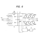
- Fig. 6 shows an example in which electrical equipment incorporates a switching power supply using a power supply system according to an embodiment of the present invention; specifically the switching power supply is used in a frequency converter.
- reference numerals D1 to D6 denote rectifying diodes for three-phase current which collectively constitute a rectifier (converter section) for receiving an AC current from an AC power supply V AC and converting it to a DC voltage.
- Reference numerals Q1 to Q6 denote inverter switching devices.
- Power transistors such as IGBTs or bipolar transistors are used as the inverter switching devices.
- Reference numerals FWD1 to FWD6 denote inverter flywheeling diodes constituting the inverter section for converting a DC intermediate voltage (P-N DC voltage) to a three-phase AC voltage whose amplitude and frequency can be arbitrarily changed.
- the inverter (or frequency converter) of the present embodiment shown in Fig. 6 has at least the above inverter section or converter section. It should be noted that the example shown in Fig. 6 is configured such that the output (voltage) of the converter section is used as the DC intermediate voltage (P-N DC voltage). However, the present embodiment is not limited to the above configuration in which the inverter has a converter section therein. Therefore, for example, the inverter may be configured such that it has no converter section and a DC intermediate voltage (P-N DC voltage) is supplied from an external power supply.
- a thyristor Thy and a resistor RD collectively constitute an inrush current blocking circuit to the capacitors C1 and C2.
- reference numerals CB1 and CB2 denote smoothing capacitors in the DC intermediate voltage section of the frequency converter.
- the two capacitors CB1 and CB2 are connected in series and voltage balancing resistors RB1 and RB2 are connected in parallel to the capacitors CB1 and CB2.
- the (power supply) PS shown in Fig. 6 is the same as that shown in Fig. 1 and is made up of a PWM control circuit CTRL, a switching device M, a transformer T, etc. (constituting a switching power supply circuit).
- the power supply PS is used as a control source for supplying a control voltage to the inverter control circuit CTRL of this frequency converter.
- a resistor R1 is connected to the connection point A at which the capacitors CB1 and CB2 are connected in series, as in Fig. 1.
- the primary winding L1 of the transformer is connected to the point P on the positive side of the DC voltage in Fig. 6 (for the power supply PS, the point P corresponds to the point B in Fig. 1).
- the point N on the negative side in Fig. 6, on the other hand, is connected to a common potential for the PWM control circuit CTRL and the switching device M.
- the values of the resistors (impedance values) connected in parallel to the capacitors CB1 and CB2 are set such that the voltages applied to the capacitors are equalized.
- This arrangement is effective in efficiently using the capacities of the capacitors CB1 and CB2 since capacitors of the same rated voltage are usually used as the capacitors CB1 and CB2.
- the voltages applied to the capacitors exceed their withstand voltages or a certain margin must be provided for these voltages. In such a case, it is necessary to install two or more capacitors connected in series.
- the embodiments of the present invention utilize this series-connection arrangement to reduce the power loss produced in the starting resistor. Therefore, it is not necessary to prepare a special capacitor for startup, resulting in a simple configuration and low cost.
- the present invention can lower the voltage applied to the resistor for supplying power to a switching power supply and thereby reduce the power loss, resulting in a reduced amount of generated heat. Furthermore, the present invention makes it possible to miniaturize the device and reduce the cost.
Landscapes
- Engineering & Computer Science (AREA)
- Power Engineering (AREA)
- Dc-Dc Converters (AREA)
- Inverter Devices (AREA)
Applications Claiming Priority (2)
| Application Number | Priority Date | Filing Date | Title |
|---|---|---|---|
| JP2002147057 | 2002-05-22 | ||
| JP2002147057A JP2003339164A (ja) | 2002-05-22 | 2002-05-22 | スイッチング電源回路、及びインバータ装置 |
Publications (2)
| Publication Number | Publication Date |
|---|---|
| EP1365499A1 true EP1365499A1 (de) | 2003-11-26 |
| EP1365499B1 EP1365499B1 (de) | 2020-02-12 |
Family
ID=29397843
Family Applications (1)
| Application Number | Title | Priority Date | Filing Date |
|---|---|---|---|
| EP03253153.5A Expired - Lifetime EP1365499B1 (de) | 2002-05-22 | 2003-05-20 | Schaltnetzteil |
Country Status (6)
| Country | Link |
|---|---|
| US (2) | US7151680B2 (de) |
| EP (1) | EP1365499B1 (de) |
| JP (1) | JP2003339164A (de) |
| KR (1) | KR100549135B1 (de) |
| CN (2) | CN1309155C (de) |
| TW (1) | TWI291804B (de) |
Cited By (1)
| Publication number | Priority date | Publication date | Assignee | Title |
|---|---|---|---|---|
| AT414188B (de) * | 2004-04-05 | 2006-10-15 | Felix Dipl Ing Dr Himmelstoss | Verlustarme dc/dc konverter |
Families Citing this family (18)
| Publication number | Priority date | Publication date | Assignee | Title |
|---|---|---|---|---|
| JP2007511994A (ja) * | 2003-11-14 | 2007-05-10 | コーニンクレッカ フィリップス エレクトロニクス エヌ ヴィ | チューナ互換性スイッチモード電源構造 |
| JP4583248B2 (ja) * | 2004-10-14 | 2010-11-17 | ローランド株式会社 | スイッチング電源装置 |
| TW200731647A (en) * | 2006-02-14 | 2007-08-16 | Asustek Comp Inc | Signal generating circuit having an electromagnetic induction device for utilizing energy stored by a snubber |
| KR101129391B1 (ko) * | 2007-08-13 | 2012-03-28 | 삼성전자주식회사 | 수동 클램프 회로를 갖는 스위칭 모드 전원공급장치 |
| US20100309689A1 (en) * | 2009-06-03 | 2010-12-09 | David Coulson | Bootstrap Circuitry |
| US8729811B2 (en) * | 2010-07-30 | 2014-05-20 | Cirrus Logic, Inc. | Dimming multiple lighting devices by alternating energy transfer from a magnetic storage element |
| CN102158067B (zh) * | 2011-04-20 | 2013-03-27 | 广州金升阳科技有限公司 | 一种开关电源的启动电路 |
| EP2792060A2 (de) | 2011-12-14 | 2014-10-22 | Cirrus Logic, Inc. | Anpassungsfähige stromsteuerungstaktung und reaktive stromsteuerung zur schnittstellenbildung mit einem dimmer |
| EP2816547A1 (de) * | 2013-06-17 | 2014-12-24 | ABB Research Ltd. | Adaptiver RCD-Dämpfer und Verfahren zur Wandlerumschaltung |
| US9654021B2 (en) | 2013-10-09 | 2017-05-16 | Rockwell Automation Technologies, Inc. | Multifunction power converter with option for integrated magnetics |
| US9161401B1 (en) | 2014-03-20 | 2015-10-13 | Cirrus Logic, Inc. | LED (light-emitting diode) string derived controller power supply |
| CN103904897B (zh) * | 2014-04-17 | 2016-08-24 | 矽力杰半导体技术(杭州)有限公司 | 开关电源控制电路、开关电源、前沿检测电路和方法 |
| CN106953533A (zh) * | 2017-03-22 | 2017-07-14 | 合肥惠科金扬科技有限公司 | 反激式电源电路和用电设备 |
| JP6886107B2 (ja) * | 2017-04-07 | 2021-06-16 | 富士通株式会社 | 電源回路 |
| US10629396B2 (en) | 2017-05-08 | 2020-04-21 | Rockwell Automation Technologies, Inc. | Arc flash resistant enclosure with segregated cooling |
| JP6832790B2 (ja) * | 2017-05-19 | 2021-02-24 | 三菱電機株式会社 | インバータ装置 |
| WO2019016990A1 (ja) | 2017-07-20 | 2019-01-24 | パナソニックIpマネジメント株式会社 | 電源装置および制御方法 |
| JP6984002B2 (ja) * | 2018-03-19 | 2021-12-17 | 三菱電機株式会社 | 抵抗装置およびインバータ装置 |
Citations (8)
| Publication number | Priority date | Publication date | Assignee | Title |
|---|---|---|---|---|
| JPS55127884A (en) | 1979-03-24 | 1980-10-03 | Meidensha Electric Mfg Co Ltd | Inverter and method for driving inverter |
| SU1282298A1 (ru) * | 1985-07-08 | 1987-01-07 | Научно-исследовательский институт электронной интроскопии при Томском политехническом институте им.С.М.Кирова | Полумостовой инвертор |
| JPS63240371A (ja) * | 1987-03-25 | 1988-10-06 | Sony Corp | スイツチング・レギユレ−タ |
| DE4029057A1 (de) * | 1990-09-13 | 1992-03-19 | Eberle A Gmbh | Anlaufversorgungsspannung fuer primaergetaktete netzteile |
| JPH07231675A (ja) | 1994-02-17 | 1995-08-29 | Murata Mfg Co Ltd | 電源回路 |
| JPH1118421A (ja) | 1997-06-27 | 1999-01-22 | Toko Inc | スイッチング電源の起動回路 |
| US5953219A (en) * | 1997-11-06 | 1999-09-14 | Murata Manufacturing Co., Ltd. | Control circuit power supply circuit and power supply circuit including same |
| WO2003030342A2 (en) * | 2001-10-02 | 2003-04-10 | Honeywell International Inc. | Soft-start of dc link capacitors for power electronics and drive systems |
Family Cites Families (15)
| Publication number | Priority date | Publication date | Assignee | Title |
|---|---|---|---|---|
| US4028596A (en) * | 1974-12-13 | 1977-06-07 | Coulter Information Systems, Inc. | Corona power supply circuit |
| JPS60189889A (ja) * | 1984-03-12 | 1985-09-27 | 松下電器産業株式会社 | 高周波加熱装置 |
| JPS6126496A (ja) | 1984-07-13 | 1986-02-05 | Fuji Electric Co Ltd | 停電時のインバ−タ運転方式 |
| US4642744A (en) * | 1984-11-26 | 1987-02-10 | Tektronix, Inc. | Regulated high voltage supply |
| JPH07111918B2 (ja) * | 1987-07-28 | 1995-11-29 | 三菱電機株式会社 | マイクロ波放電光源装置 |
| JPH0270268A (ja) | 1988-09-01 | 1990-03-09 | Murata Mfg Co Ltd | スイッチングレギュレータ |
| US5043598A (en) * | 1988-09-20 | 1991-08-27 | Tdk Corporation | High voltage supply having a voltage stabilizer |
| US5003454A (en) * | 1990-01-09 | 1991-03-26 | North American Philips Corporation | Power supply with improved power factor correction |
| DE4125510A1 (de) | 1991-08-01 | 1993-02-04 | Philips Patentverwaltung | Schaltungsanordnung mit einem schaltnetzteil |
| JP2677075B2 (ja) | 1991-08-30 | 1997-11-17 | 富士電機株式会社 | ハーフブリッジ形電力変換回路 |
| KR960013948B1 (ko) * | 1993-11-16 | 1996-10-10 | 삼성전자 주식회사 | 역률 보정회로 |
| US5796296A (en) * | 1996-10-07 | 1998-08-18 | Texas Instruments Incorporated | Combined resistance-capacitance ladder voltage divider circuit |
| JP4114238B2 (ja) | 1998-08-12 | 2008-07-09 | ソニー株式会社 | スイッチングレギュレータ |
| JP2000262057A (ja) | 1999-03-10 | 2000-09-22 | Tokimec Inc | 制御用補助電源の起動回路 |
| JP2001095247A (ja) * | 1999-09-21 | 2001-04-06 | Sony Corp | スイッチング電源回路 |
-
2002
- 2002-05-22 JP JP2002147057A patent/JP2003339164A/ja active Pending
-
2003
- 2003-05-06 TW TW092112362A patent/TWI291804B/zh not_active IP Right Cessation
- 2003-05-20 EP EP03253153.5A patent/EP1365499B1/de not_active Expired - Lifetime
- 2003-05-21 KR KR1020030032224A patent/KR100549135B1/ko not_active Expired - Fee Related
- 2003-05-22 US US10/444,762 patent/US7151680B2/en not_active Expired - Lifetime
- 2003-05-22 CN CNB031368743A patent/CN1309155C/zh not_active Expired - Lifetime
- 2003-05-22 CN CNA200710006510XA patent/CN101030730A/zh active Pending
-
2006
- 2006-11-13 US US11/599,220 patent/US7394668B2/en not_active Expired - Lifetime
Patent Citations (8)
| Publication number | Priority date | Publication date | Assignee | Title |
|---|---|---|---|---|
| JPS55127884A (en) | 1979-03-24 | 1980-10-03 | Meidensha Electric Mfg Co Ltd | Inverter and method for driving inverter |
| SU1282298A1 (ru) * | 1985-07-08 | 1987-01-07 | Научно-исследовательский институт электронной интроскопии при Томском политехническом институте им.С.М.Кирова | Полумостовой инвертор |
| JPS63240371A (ja) * | 1987-03-25 | 1988-10-06 | Sony Corp | スイツチング・レギユレ−タ |
| DE4029057A1 (de) * | 1990-09-13 | 1992-03-19 | Eberle A Gmbh | Anlaufversorgungsspannung fuer primaergetaktete netzteile |
| JPH07231675A (ja) | 1994-02-17 | 1995-08-29 | Murata Mfg Co Ltd | 電源回路 |
| JPH1118421A (ja) | 1997-06-27 | 1999-01-22 | Toko Inc | スイッチング電源の起動回路 |
| US5953219A (en) * | 1997-11-06 | 1999-09-14 | Murata Manufacturing Co., Ltd. | Control circuit power supply circuit and power supply circuit including same |
| WO2003030342A2 (en) * | 2001-10-02 | 2003-04-10 | Honeywell International Inc. | Soft-start of dc link capacitors for power electronics and drive systems |
Non-Patent Citations (4)
| Title |
|---|
| PATENT ABSTRACTS OF JAPAN vol. 004, no. 185 (E - 038) 19 December 1980 (1980-12-19) * |
| PATENT ABSTRACTS OF JAPAN vol. 013, no. 046 (E - 711) 2 February 1989 (1989-02-02) * |
| PATENT ABSTRACTS OF JAPAN vol. 1995, no. 11 26 December 1995 (1995-12-26) * |
| PATENT ABSTRACTS OF JAPAN vol. 1999, no. 04 30 April 1999 (1999-04-30) * |
Cited By (1)
| Publication number | Priority date | Publication date | Assignee | Title |
|---|---|---|---|---|
| AT414188B (de) * | 2004-04-05 | 2006-10-15 | Felix Dipl Ing Dr Himmelstoss | Verlustarme dc/dc konverter |
Also Published As
| Publication number | Publication date |
|---|---|
| TWI291804B (en) | 2007-12-21 |
| CN1309155C (zh) | 2007-04-04 |
| KR100549135B1 (ko) | 2006-02-03 |
| JP2003339164A (ja) | 2003-11-28 |
| US7394668B2 (en) | 2008-07-01 |
| TW200308138A (en) | 2003-12-16 |
| CN1474501A (zh) | 2004-02-11 |
| US20040066661A1 (en) | 2004-04-08 |
| KR20030091723A (ko) | 2003-12-03 |
| US7151680B2 (en) | 2006-12-19 |
| CN101030730A (zh) | 2007-09-05 |
| EP1365499B1 (de) | 2020-02-12 |
| US20070058400A1 (en) | 2007-03-15 |
Similar Documents
| Publication | Publication Date | Title |
|---|---|---|
| US7151680B2 (en) | Switching power supply circuit and frequency converter | |
| US8138694B2 (en) | Bidirectional buck-boost power converters | |
| US20170237355A1 (en) | Dc-to-dc converter comprising a transformer | |
| US9246399B2 (en) | Power supply system and control method thereof | |
| US5825639A (en) | DC bus capacitor arrangement | |
| US6977445B2 (en) | Three phase rectifier circuit with virtual neutral | |
| EP0083717B1 (de) | Gleichstromnetzgerät | |
| US6900996B2 (en) | Method and apparatus for controlling a DC-DC converter | |
| US6023419A (en) | Capacitor regulated controllable voltage and current power supply | |
| WO2021028041A1 (en) | Direct current power supply assembly | |
| KR20110135126A (ko) | 캐스케이드 멀티레벨 고압인버터의 돌입전류 방지장치 | |
| US11283364B2 (en) | Power supply and power system having a step-down circuit and an inverse-conversion circuit | |
| US10164538B1 (en) | Dual-capacitors-based AC line frequency low voltage DC power supply circuit | |
| US20090027923A1 (en) | Power supply device and power supply control method | |
| EP1693949B1 (de) | Elektrische stromwandlervorrichtung | |
| JP2011167068A (ja) | スイッチング電源回路、及びインバータ装置 | |
| KR102730094B1 (ko) | 외부전원으로부터 공급되는 과전압을 차단하는 전력 변환 장치 | |
| JP2011050137A (ja) | 電力変換回路 | |
| RU2808233C1 (ru) | Ключевой нормализатор фазного тока | |
| US11424618B2 (en) | Converter, arrangement comprising a converter and method for operating same | |
| JP2008125355A (ja) | スイッチング電源回路、及びインバータ装置 | |
| JP2000354368A (ja) | スイッチング電源装置 | |
| JP2000184720A (ja) | コンバータ及びインバータ装置 | |
| JPH06245526A (ja) | 直流高電圧電源装置 | |
| EP1246352A2 (de) | Wechselrichterstromversorgungsgerät |
Legal Events
| Date | Code | Title | Description |
|---|---|---|---|
| PUAI | Public reference made under article 153(3) epc to a published international application that has entered the european phase |
Free format text: ORIGINAL CODE: 0009012 |
|
| 17P | Request for examination filed |
Effective date: 20030610 |
|
| AK | Designated contracting states |
Kind code of ref document: A1 Designated state(s): AT BE BG CH CY CZ DE DK EE ES FI FR GB GR HU IE IT LI LU MC NL PT RO SE SI SK TR |
|
| AX | Request for extension of the european patent |
Extension state: AL LT LV MK |
|
| AKX | Designation fees paid |
Designated state(s): DE FR GB |
|
| 17Q | First examination report despatched |
Effective date: 20070108 |
|
| RIC1 | Information provided on ipc code assigned before grant |
Ipc: H02M 1/00 20060101AFI20030916BHEP |
|
| REG | Reference to a national code |
Ref country code: DE Ref legal event code: R079 Ref document number: 60352385 Country of ref document: DE Free format text: PREVIOUS MAIN CLASS: H02M0001000000 Ipc: H02M0001360000 |
|
| GRAP | Despatch of communication of intention to grant a patent |
Free format text: ORIGINAL CODE: EPIDOSNIGR1 |
|
| STAA | Information on the status of an ep patent application or granted ep patent |
Free format text: STATUS: GRANT OF PATENT IS INTENDED |
|
| RIC1 | Information provided on ipc code assigned before grant |
Ipc: H02M 1/36 20070101AFI20190909BHEP |
|
| INTG | Intention to grant announced |
Effective date: 20191008 |
|
| GRAS | Grant fee paid |
Free format text: ORIGINAL CODE: EPIDOSNIGR3 |
|
| GRAA | (expected) grant |
Free format text: ORIGINAL CODE: 0009210 |
|
| STAA | Information on the status of an ep patent application or granted ep patent |
Free format text: STATUS: THE PATENT HAS BEEN GRANTED |
|
| REG | Reference to a national code |
Ref country code: DE Ref legal event code: R082 Ref document number: 60352385 Country of ref document: DE Representative=s name: MEWBURN ELLIS LLP, DE |
|
| AK | Designated contracting states |
Kind code of ref document: B1 Designated state(s): DE FR GB |
|
| REG | Reference to a national code |
Ref country code: GB Ref legal event code: FG4D |
|
| REG | Reference to a national code |
Ref country code: DE Ref legal event code: R096 Ref document number: 60352385 Country of ref document: DE |
|
| REG | Reference to a national code |
Ref country code: DE Ref legal event code: R097 Ref document number: 60352385 Country of ref document: DE |
|
| PLBE | No opposition filed within time limit |
Free format text: ORIGINAL CODE: 0009261 |
|
| STAA | Information on the status of an ep patent application or granted ep patent |
Free format text: STATUS: NO OPPOSITION FILED WITHIN TIME LIMIT |
|
| 26N | No opposition filed |
Effective date: 20201113 |
|
| GBPC | Gb: european patent ceased through non-payment of renewal fee |
Effective date: 20200520 |
|
| PG25 | Lapsed in a contracting state [announced via postgrant information from national office to epo] |
Ref country code: GB Free format text: LAPSE BECAUSE OF NON-PAYMENT OF DUE FEES Effective date: 20200520 |
|
| PGFP | Annual fee paid to national office [announced via postgrant information from national office to epo] |
Ref country code: FR Payment date: 20220408 Year of fee payment: 20 Ref country code: DE Payment date: 20220329 Year of fee payment: 20 |
|
| REG | Reference to a national code |
Ref country code: DE Ref legal event code: R071 Ref document number: 60352385 Country of ref document: DE |