EP1376703A2 - Dispositif semi-conducteur à grille isolée et sa méthode de fabrication - Google Patents
Dispositif semi-conducteur à grille isolée et sa méthode de fabrication Download PDFInfo
- Publication number
- EP1376703A2 EP1376703A2 EP01126332A EP01126332A EP1376703A2 EP 1376703 A2 EP1376703 A2 EP 1376703A2 EP 01126332 A EP01126332 A EP 01126332A EP 01126332 A EP01126332 A EP 01126332A EP 1376703 A2 EP1376703 A2 EP 1376703A2
- Authority
- EP
- European Patent Office
- Prior art keywords
- igbt
- semiconductor layer
- region
- semiconductor
- type
- Prior art date
- Legal status (The legal status is an assumption and is not a legal conclusion. Google has not performed a legal analysis and makes no representation as to the accuracy of the status listed.)
- Withdrawn
Links
Images


Classifications
-
- H—ELECTRICITY
- H10—SEMICONDUCTOR DEVICES; ELECTRIC SOLID-STATE DEVICES NOT OTHERWISE PROVIDED FOR
- H10D—INORGANIC ELECTRIC SEMICONDUCTOR DEVICES
- H10D18/00—Thyristors
- H10D18/60—Gate-turn-off devices
- H10D18/65—Gate-turn-off devices with turn-off by field effect
- H10D18/655—Gate-turn-off devices with turn-off by field effect produced by insulated gate structures
-
- H—ELECTRICITY
- H10—SEMICONDUCTOR DEVICES; ELECTRIC SOLID-STATE DEVICES NOT OTHERWISE PROVIDED FOR
- H10D—INORGANIC ELECTRIC SEMICONDUCTOR DEVICES
- H10D12/00—Bipolar devices controlled by the field effect, e.g. insulated-gate bipolar transistors [IGBT]
- H10D12/01—Manufacture or treatment
- H10D12/031—Manufacture or treatment of IGBTs
- H10D12/032—Manufacture or treatment of IGBTs of vertical IGBTs
- H10D12/038—Manufacture or treatment of IGBTs of vertical IGBTs having a recessed gate, e.g. trench-gate IGBTs
-
- H—ELECTRICITY
- H10—SEMICONDUCTOR DEVICES; ELECTRIC SOLID-STATE DEVICES NOT OTHERWISE PROVIDED FOR
- H10D—INORGANIC ELECTRIC SEMICONDUCTOR DEVICES
- H10D12/00—Bipolar devices controlled by the field effect, e.g. insulated-gate bipolar transistors [IGBT]
- H10D12/411—Insulated-gate bipolar transistors [IGBT]
- H10D12/441—Vertical IGBTs
- H10D12/461—Vertical IGBTs having non-planar surfaces, e.g. having trenches, recesses or pillars in the surfaces of the emitter, base or collector regions
- H10D12/481—Vertical IGBTs having non-planar surfaces, e.g. having trenches, recesses or pillars in the surfaces of the emitter, base or collector regions having gate structures on slanted surfaces, on vertical surfaces, or in grooves, e.g. trench gate IGBTs
-
- H—ELECTRICITY
- H10—SEMICONDUCTOR DEVICES; ELECTRIC SOLID-STATE DEVICES NOT OTHERWISE PROVIDED FOR
- H10D—INORGANIC ELECTRIC SEMICONDUCTOR DEVICES
- H10D18/00—Thyristors
- H10D18/40—Thyristors with turn-on by field effect
-
- H—ELECTRICITY
- H10—SEMICONDUCTOR DEVICES; ELECTRIC SOLID-STATE DEVICES NOT OTHERWISE PROVIDED FOR
- H10D—INORGANIC ELECTRIC SEMICONDUCTOR DEVICES
- H10D62/00—Semiconductor bodies, or regions thereof, of devices having potential barriers
- H10D62/10—Shapes, relative sizes or dispositions of the regions of the semiconductor bodies; Shapes of the semiconductor bodies
- H10D62/102—Constructional design considerations for preventing surface leakage or controlling electric field concentration
- H10D62/103—Constructional design considerations for preventing surface leakage or controlling electric field concentration for increasing or controlling the breakdown voltage of reverse-biased devices
- H10D62/105—Constructional design considerations for preventing surface leakage or controlling electric field concentration for increasing or controlling the breakdown voltage of reverse-biased devices by having particular doping profiles, shapes or arrangements of PN junctions; by having supplementary regions, e.g. junction termination extension [JTE]
- H10D62/106—Constructional design considerations for preventing surface leakage or controlling electric field concentration for increasing or controlling the breakdown voltage of reverse-biased devices by having particular doping profiles, shapes or arrangements of PN junctions; by having supplementary regions, e.g. junction termination extension [JTE] having supplementary regions doped oppositely to or in rectifying contact with regions of the semiconductor bodies, e.g. guard rings with PN or Schottky junctions
-
- H—ELECTRICITY
- H10—SEMICONDUCTOR DEVICES; ELECTRIC SOLID-STATE DEVICES NOT OTHERWISE PROVIDED FOR
- H10D—INORGANIC ELECTRIC SEMICONDUCTOR DEVICES
- H10D62/00—Semiconductor bodies, or regions thereof, of devices having potential barriers
- H10D62/10—Shapes, relative sizes or dispositions of the regions of the semiconductor bodies; Shapes of the semiconductor bodies
- H10D62/17—Semiconductor regions connected to electrodes not carrying current to be rectified, amplified or switched, e.g. channel regions
- H10D62/192—Base regions of thyristors
- H10D62/206—Cathode base regions of thyristors
-
- H—ELECTRICITY
- H10—SEMICONDUCTOR DEVICES; ELECTRIC SOLID-STATE DEVICES NOT OTHERWISE PROVIDED FOR
- H10D—INORGANIC ELECTRIC SEMICONDUCTOR DEVICES
- H10D62/00—Semiconductor bodies, or regions thereof, of devices having potential barriers
- H10D62/10—Shapes, relative sizes or dispositions of the regions of the semiconductor bodies; Shapes of the semiconductor bodies
- H10D62/17—Semiconductor regions connected to electrodes not carrying current to be rectified, amplified or switched, e.g. channel regions
- H10D62/393—Body regions of DMOS transistors or IGBTs
-
- H—ELECTRICITY
- H10—SEMICONDUCTOR DEVICES; ELECTRIC SOLID-STATE DEVICES NOT OTHERWISE PROVIDED FOR
- H10D—INORGANIC ELECTRIC SEMICONDUCTOR DEVICES
- H10D64/00—Electrodes of devices having potential barriers
- H10D64/20—Electrodes characterised by their shapes, relative sizes or dispositions
- H10D64/23—Electrodes carrying the current to be rectified, amplified, oscillated or switched, e.g. sources, drains, anodes or cathodes
- H10D64/231—Emitter or collector electrodes for bipolar transistors
-
- H—ELECTRICITY
- H10—SEMICONDUCTOR DEVICES; ELECTRIC SOLID-STATE DEVICES NOT OTHERWISE PROVIDED FOR
- H10D—INORGANIC ELECTRIC SEMICONDUCTOR DEVICES
- H10D64/00—Electrodes of devices having potential barriers
- H10D64/20—Electrodes characterised by their shapes, relative sizes or dispositions
- H10D64/23—Electrodes carrying the current to be rectified, amplified, oscillated or switched, e.g. sources, drains, anodes or cathodes
- H10D64/251—Source or drain electrodes for field-effect devices
- H10D64/252—Source or drain electrodes for field-effect devices for vertical or pseudo-vertical devices
-
- H—ELECTRICITY
- H10—SEMICONDUCTOR DEVICES; ELECTRIC SOLID-STATE DEVICES NOT OTHERWISE PROVIDED FOR
- H10W—GENERIC PACKAGES, INTERCONNECTIONS, CONNECTORS OR OTHER CONSTRUCTIONAL DETAILS OF DEVICES COVERED BY CLASS H10
- H10W72/00—Interconnections or connectors in packages
- H10W72/90—Bond pads, in general
- H10W72/921—Structures or relative sizes of bond pads
- H10W72/926—Multiple bond pads having different sizes
Definitions
- the present invention relates to an insulated gate semiconductor device such as an insulated gate bipolar transistor (referred to as an IGBT hereinafter) and a method of fabricating the same.
- an IGBT insulated gate bipolar transistor
- An insulated gate semiconductor device comprises a plurality of p type and n type semiconductor layers alternately joined together in series such that the semiconductor layers at opposite ends are electrically connected to positive and negative main electrodes, respectively, and at least one of the other semiconductor layers is joined to a gate electrode applying an electric field through an insulator.
- an IGBT comprises a multiplicity of IGBT elements (referred to as IGBT cells hereinafter) connected in parallel.
- Fig. 32 is a cross sectional view showing a basic structure of an IGBT cell forming the IGBT.
- a p + semiconductor layer 1 is formed of a p type semiconductor substrate and has first and second major surfaces, and an n + buffer layer 2 is formed on the first major surface of the p + semiconductor layer 1.
- An n - semiconductor layer 3 is formed over the n + buffer layer 2.
- p type base regions 4 are formed in a partial surface region of the n - semiconductor layer 3 by selective diffusion of p type impurities.
- n + emitter regions 5 are formed in a partial region of the p type base regions 4 by selective diffusion of a high concentration of n type impurities.
- Upper surfaces of the p type base regions 4 between the surface of the n - semiconductor layer 3 and the surfaces of the n + emitter regions 5 serve as channel regions 6.
- a gate insulation film 7 is formed on the channel regions 6.
- a gate electrode 8 made of, for example, polycrystalline silicon is formed on the gate insulation film 7.
- Emitter electrodes 9 made of, for example, aluminum are formed over the respective upper surfaces of the p type base regions 4 and the n + emitter regions 5.
- the gate electrode 8 and the emitter electrodes 9 are insulated from each other.
- Gate electrodes 9 for all IGBT cells are electrically connected to each other, and emitter electrodes 9 for all IGBT cells are electrically connected to each other.
- a collector electrode 10 made of aluminum or the like is formed on the second major surface of the p + semiconductor layer 1.
- the collector electrode 10 is formed integrally for all IGBT cells.
- a predetermined collector voltage V CE is initially applied between the emitter electrodes 9 and the collector electrode 10.
- V GE exceeds a threshold value
- the channel regions 6 are inverted into n type, and n type channels are formed in the channel regions 6.
- Electrons as carriers are emitted from the emitter electrodes 9 through the n type channels into the n - semiconductor layer 3.
- the emitted electrons causes forward bias between the p + semiconductor layer 1 and the n - semiconductor layer 3 (including the n + buffer layer 2), and holes as carriers are emitted from the p + semiconductor layer 1.
- the resistance of the n - semiconductor layer 3 decreases significantly and a collector current I C flowing from the collector electrode 10 to the emitter electrodes 9 reaches a high value. That is, the IGBT comes into conduction (turns on).
- the resistance relative to the collector current I C at this time is represented as an ON resistance.
- the ON resistance is normally indicated by a saturation collector voltage V CE (sat) at the time when the collector current I C has a rated current value. In this manner, the IGBT decreases the resistance of the n - semiconductor layer 3 by emitting holes from the p + semiconductor layer 1 to increase a current-carrying capacity.
- the IGBT comprises a parasitic bipolar transistor consisting of the n + emitter region 5, the p type base region 4 and the n - semiconductor layer 3.
- This parasitic bipolar transistor generally turns on when the hole current flowing in the p type base region 4 exceeds a value. Turning on of the parasitic bipolar transistor causes a parasitic thyristor consisting of the n + emitter region 5, the p type base region 4, the n - semiconductor layer 3, and the p + semiconductor layer 1 to turn on (referred to as latch-up of the IGBT).
- the gate voltage V GE can no longer control the current (collector current I C ) flowing in the IGBT which is then broken down.
- the breakdown due to latch-up is considered to be liable to occur at specific positions of the IGBT.
- Fig. 33 is a plan view of a common IGBT.
- a rectangular gate pad GP is provided in the lower middle of the IGBT.
- Gate lines GL extend from upper and lower portions of the gate pad GP.
- the gate line GL from the upper portion extends along the centerline of the IGBT up to a location slightly above the center, and the gate line GL from the lower portion is formed in such a manner as to surround the outer periphery of the IGBT.
- the emitter electrode 9 is formed in a region enclosed by the central and outer peripheral gate lines GL.
- IGBT cell regions serving as an active region are indicated by the broken lines of Fig. 33.
- a p type semiconductor region 11 is formed so as to surround the IGBT cell regions.
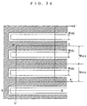
- Fig. 34 is an enlarged view of a region X enclosed by the dashed-and-dotted lines of Fig. 33, with portions of the emitter electrode 9 removed.
- a multiplicity of IGBT cells are spaced a constant distance W cel from each other in parallel within a corner portion indicated by the lines C-O-C', each of the IGBT cells including a stripe-shaped contact hole having a width W ch1 .
- the p type semiconductor region 11 including a stripe-shaped contact hole having the width W ch1 is formed outside the corner portion shown by the lines C-O-C'.
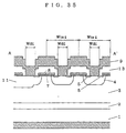
- Fig. 35 is a sectional view taken along the line A-A' of Fig. 34
- Fig. 36 is a sectional view taken along the line B-B' thereof.
- Fig. 35 illustrates the IGBT cells described with reference to Fig. 32 which are arranged in parallel such that the emitter electrodes 9 are connected to upper surfaces of the p type base regions 4 and n + emitter regions 5 of the respective IGBT cells through the contact holes having the width W ch1 .
- a portion adjacent the side A of Fig. 35 represents a region outside the line C-O of the comer portion indicated by the lines C-O-C' wherein the p type semiconductor region 11 is formed in the surface of the n - semiconductor layer 3 by double diffusion in corresponding to the p type base region 4 of the adjacent IGBT cell.
- the emitter electrode 9 is connected to the upper surface of the p type semiconductor region 11 through the contact hole having the width W ch1 .
- the p type semiconductor region 11 is much larger than the p type base region 4.
- Fig. 36 is a sectional view taken longitudinally of the stripe-shaped contact hole.
- the p type base region 4 extends in the longitudinal direction of the contact hole, and the emitter electrode 9 extends longitudinally for connection to the p type base region 4.
- a portion adjacent the side B represents a region outside the line O-C' of the corner portion indicated by the lines C-O-C'.
- the p type semiconductor region 11 is shown as overlapping the p type base region 4.
- the IGBT cell adjacent the p type semiconductor region 11 conducts more hole current than other IGBT cells, and the parasitic thyristor consisting of the n + emitter region 5, the p type base region 4, the n - semiconductor layer 3 and the p + semiconductor layer 1 turns on as above described to cause latch-up of the IGBT. Then the current (collector current I c ) flowing in the IGBT is not controlled and the IGBT is broken down.
- Such a phenomenon often occurs during transition from the ON state to the OFF state.
- turning off of the gate electrode 8 causes electrons to stop being supplied from the emitter electrode 9 to stop the supply of holes from the p + semiconductor layer 1.
- the electrons and holes left in the n - semiconductor layer 3 (including the n + buffer layer 2) move toward the collector electrode 10 and the emitter electrodes 9, respectively.
- the holes remain after the electrons pass through to the collector electrode 10.
- the holes which disappear by recombination with electrons in the ON state also move toward the emitter electrodes 9.
- Fig. 37 is a graph showing changes with time in current flowing in the IGBT when the IGBT makes an ON-state to OFF-state transition, the abscissa of the graph being time, the ordinate thereof being current value.
- the electron current decreases rapidly during the time interval between 1.98 ⁇ sec. and 2.06 ⁇ sec.
- the hole current increases rapidly from about 2.02 ⁇ sec. to provide a more than 1.5X increase in hole current.
- Fig. 38 is an enlarged schematic view of Fig. 35.
- the carrier density is uniform within an IGBT cell as illustrated in Fig. 38. It is assumed that carriers extend at an angle of about 45 degrees from a cell end under the p type semiconductor region 11 as shown in Fig. 38.
- the thickness of the n - semiconductor layer 3 is designated as t n-
- the depth of the p type base region 4 of the IGBT cell is designated as P xj
- the width of the IGBT cell is designated as W cel .
- the number of carriers C1 in a region defined by the centerline G of the gate electrode 8 and the centerline S of the IGBT cell is approximately expressed as: C1 ⁇ 1 2 ( W cel ⁇ ( t n - - P xj ))
- the number of carriers C2 in a region defined by the centerline G of the gate electrode 8 and the line L 45 indicative of spreading of the carriers is approximately expressed as: C2 ⁇ 1 2 ( W cel ⁇ ( t n - - P xj )) + 1 2 ( t n - - 1 2 W cel ) 2
- 1/2W ch(cel) is the size
- the area of the emitter electrode 9 connected to the p type semiconductor region 11 decreases with size reduction of the IGBT cell, and the holes supplied from the p + semiconductor layer 1 directly below the p type semiconductor region 11 are difficult to pass through to the emitter electrode 9. This also results in IGBT breakdown.
- an insulated gate semiconductor device comprises: a first semiconductor layer of a first conductivity type and having a relatively low concentration; a plurality of stripe-shaped second semiconductor layers of a second conductivity type selectively formed in parallel in a surface of the first semiconductor layer; a plurality of third semiconductor layers of the first conductivity type and having a relatively high concentration, the third semiconductor layers being selectively formed in respective surfaces of the second semiconductor layers; a plurality of stripe-shaped insulating layers formed on upper surfaces of the first and second semiconductor layers between ends of the third semiconductor layers in the second semiconductor layers; a plurality of stripe-shaped control electrodes formed on the insulating layers; a plurality of layer insulating films covering the control electrodes; the first semiconductor layer, the second semiconductor layers, the third semiconductor layers, the insulating layers, the control electrodes, and the layer insulating films forming an active region; a fourth semiconductor layer of the second conductivity type formed in the surface of the first semiconductor layer so as to enclose the active region; and a plurality of
- an insulated gate semiconductor device comprises: a first semiconductor layer of a first conductivity type and having a relatively low concentration; a plurality of stripe-shaped second semiconductor layers of a second conductivity type selectively formed in parallel in a surface of the first semiconductor layer; a plurality of third semiconductor layers of the first conductivity type and having a relatively high concentration, the third semiconductor layers being selectively formed in respective surfaces of the second semiconductor layers; a plurality of insulating films formed on upper surfaces of the third semiconductor layers and on inner wall surfaces of a plurality of stripe-shaped grooves extending from the upper surface of the third semiconductor layers in the second semiconductor layers through the second semiconductor layers into the first semiconductor layer; a plurality of stripe-shaped control electrodes formed in the grooves having the inner wall surfaces on which the insulating films are formed; a plurality of layer insulating films covering the control electrodes and the insulating films; the first semiconductor layer, the second semiconductor layers, the third semiconductor layers, the insulating films, the control electrodes, and the layer
- the width of the main electrodes formed on the upper surface of the fourth semiconductor layer adjacent the active region is greater than the main electrodes within the active region, thereby to increase the amount of carrier current flowing into the main electrodes and reduce the amount of carrier current concentrated on the main electrodes within the active region adjacent the fourth semiconductor layer, preventing device breakdown due to operation of the parasitic thyristor when the device is on and changes from the ON state to OFF state.
- the main electrodes and control electrodes are reduced in size in the active region, the main electrodes formed on the upper surface of the fourth semiconductor layer adjacent the active region can be wide, to reduce the amount of carrier current concentrated on the main electrodes within the active region adjacent the fourth semiconductor layer and prevent device breakdown due to operation of the parasitic thyristor.
- the first semiconductor layer has a thickness which is not less than five times a distance between centerlines of the control electrodes adjacent to each other.
- the effects by the insulated gate semiconductor device are pronounced when the thickness of the first semiconductor layer is not less than five times the distance between the centerlines of adjacent control electrodes.
- the third semiconductor layers are not formed in the second semiconductor layers adjacent the fourth semiconductor layer.
- the insulated gate semiconductor device further comprises: a fifth semiconductor layer of the second conductivity type and having a relatively high concentration, the fifth semiconductor layer being formed in the upper surface of the fourth semiconductor layer below the second main electrodes.
- the contact resistance with the main electrodes formed on the upper surface of the fourth semiconductor layer is reduced to promote a carrier current flow, to reduce the amount of carrier current concentrated on the main electrodes within the active region adjacent the fourth semiconductor layer, preventing the device breakdown due to operation of the parasitic thyristor.
- the present invention is also intended for a method of fabricating an insulated gate semiconductor device.
- the method comprises the steps of: (a) providing a first semiconductor layer of a first conductivity type and having a relatively low concentration; (b) forming an insulating film on a surface of the first semiconductor layer and then forming a conductive layer on the insulating film; (c) patterning the conductive layer to form a plurality of stripe-shaped control electrodes; (d) implanting an impurity of a second conductivity type by using the control electrodes as a mask to form a plurality of stripe-shaped second semiconductor layers of the second conductivity type between the control electrodes; (e) implanting an impurity of the first conductivity type into the second semiconductor layers to selectively form third semiconductor layers of the first conductivity type; (f) implanting an impurity of the second conductivity type into a predetermined portion of the first semiconductor layer to form a fourth semiconductor layer of the second conductivity type; (g) forming layer insulating films so as to
- This method is suitable for fabrication of the insulated gate semiconductor device of the present invention.
- the step (f) is performed after the step (a).
- a mask is used in the step (e) which mask is designed such that the third semiconductor layers are not formed in the second semiconductor layers adjacent the fourth semiconductor layer.
- the parasitic thyristor is not formed adjacent the fourth semiconductor layer. If the carrier current is concentrated on the main electrodes within the active region adjacent the fourth semiconductor layer, the method is provided which is suitable for fabrication of the insulated gate semiconductor device that prevents the device breakdown due to operation of the parasitic thyristor.
- the method further comprises the step of: implanting an impurity of the second conductivity type into the fourth semiconductor layer to form a stripe-shaped fifth semiconductor layer of the second conductivity type prior to the step (e).
- the formation of the stripe-shaped fifth semiconductor layer of the second conductivity type in the fourth semiconductor layer can promote a carrier current flow to reduce the carrier current concentrated on the main electrodes within the active region adjacent the fourth semiconductor layer.
- the method is provided which is suitable for fabrication of the insulated gate semiconductor device that prevents the device breakdown due to operation of the parasitic thyristor.
- the method comprises the steps of: (a) providing a first semiconductor layer of a first conductivity type and having a relatively low concentration; (b) implanting an impurity of a second conductivity type into a surface of the first semiconductor layer to form a second semiconductor layer of the second conductivity type; (c) implanting an impurity of the first conductivity type into a surface of the second semiconductor layer to selectively form third semiconductor layers of the first conductivity type; (d) forming a plurality of stripe-shaped grooves extending from an upper surface of the third semiconductor layer through the second and third semiconductor layers into the first semiconductor layer; (e) forming an insulating film on inner wall surfaces of the grooves and the upper surfaces of the second and third semiconductor layers; (f) forming a conductive layer in the grooves and on an upper surface of the insulating film; (g) patterning the conductive layer to form a plurality of stripe-shaped control electrodes; (h) implanting an impurity of the second conductivity type into a pre
- This method is suitable for fabrication of the insulated gate semiconductor device of the present invention.
- the step (h) is performed after the step (a).
- a mask is used in the step (c) which mask is designed such that the third semiconductor layers are not formed in the second semiconductor layer adjacent the fourth semiconductor layer.
- the parasitic thyristor is not formed adjacent the fourth semiconductor layer. If the carrier current is concentrated on the main electrodes within the active region adjacent the fourth semiconductor layer, the method is provided which is suitable for fabrication of the insulated gate semiconductor device that prevents the device breakdown due to operation of the parasitic thyristor.
- the method further comprises the step of: implanting an impurity of the second conductivity type into the fourth semiconductor layer to form a stripe-shaped fifth semiconductor layer of the second conductivity type prior to the step (d).
- the formation of the stripe-shaped fifth semiconductor layer of the second conductivity type in the fourth semiconductor layer can promote a carrier current flow to reduce the carrier current concentrated on the main electrodes within the active region adjacent the fourth semiconductor layer.
- the method is provided which is suitable for fabrication of the insulated gate semiconductor device that prevents the device breakdown due to operation of the parasitic thyristor.
- Fig. 1 is an enlarged view of a portion corresponding to the region X enclosed by the dashed-and-dotted lines of Fig. 33 used for description of the conventional IGBT.
- stripe-shaped IGBT cells each including a contact hole CH 1 having a width W ch1 are spaced a constant distance W cel from each other in parallel inside a corner portion indicated by the lines C-O-C'.
- a p type semiconductor region 11 including a stripe-shaped contact hole CH p having a width W ch2 is formed outside the corner portion indicated by the lines C-O-C'.
- Fig. 2 is a sectional view taken along the line A-A' of Fig. 1.
- Fig. 2 illustrates the IGBT cells described with reference to Fig. 32 which are arranged in parallel such that emitter electrodes 9 are connected to upper surfaces of p type base regions 4 and n + emitter regions 5 of the respective IGBT cells through the contact holes CH 1 having the width W ch1 .
- the IGBT constructed as shown in Fig. 2 is adapted such that holes supplied from the p + semiconductor layer 1 directly below the p type semiconductor region 11 pass through the contact hole CH p having the width W ch2 in the p type semiconductor region 11 to the emitter electrodes 9 when the IGBT is on.
- the width W ch2 of the contact hole CH p in the p type semiconductor region 11 is large enough to permit the hole current in the region defined by the line L 45 of Fig.
- size reduction of the IGBT cells does not interfere with the large width W ch2 of the contact hole CH p on the p type semiconductor region 11.
- the width of the IGBT cells reduced in size is less than the thickness of the n - semiconductor layer 3 and more current flows in the contact hole CH p than in the contact hole CH 1 , also prevented is the stronger likelihood of the breakdown of the IGBT cell adjacent the p type semiconductor region 11 than that of other IGBT cells due to latch-up.
- the first preferred embodiment functions effectively when the ratio of the IGBT cell width to the thickness of the n - semiconductor layer 3 which indicates the degree of size reduction of the IGBT cell is not less than 1 to 5.
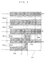
- Fig. 3 is an enlarged view of the region Y.
- the gate pad GP adjacent the corner portion is formed perpendicularly to the IGBT cells, which causes the p type semiconductor region 11 to protrude to form a recessed IGBT cell region.
- This preferred embodiment provides the contact hole CH p wider than the contact holes CH 1 in the protruding p type semiconductor region 11 parallel to the IGBT cells without changing the arrangement of the IGBT cells and permits contact between the emitter electrodes 9 and the p type semiconductor region 11 through the contact hole CH p .
- the stripe-shaped IGBT cells each including the contact hole CH 1 having the width W ch1 are spaced the constant distance W cel from each other in parallel outside the corner portion indicated by the lines C-O-C'.
- the p type semiconductor region 11 including the stripe-shaped contact hole CH p having the width W ch2 is formed inside the corner portion indicated by the lines C-O-C'.
- the section taken along the line A-A' of Fig. 3 is similar to that of Fig. 2.
- this application exhibits effects when the IGBT is on, when the IGBT makes the ON-state to OFF-state transition, and when the IGBT cells are reduced in size, similar to the application of this preferred embodiment to the region X.
- Figs. 4 to 9 are sectional views showing process steps for fabrication of the IGBT of Fig. 2 in sequential order.
- the p + semiconductor layer 1 serving as a substrate e.g., a single crystal Si substrate
- the n + buffer layer 2 and the n - semiconductor layer 3 are sequentially formed on the first major surface of the p + semiconductor layer 1 by epitaxial growth technique.
- p type impurities e.g., boron
- p type impurities are implanted into a predetermined portion of the n - semiconductor layer 3 and are then annealed to form the p type semiconductor region 11.
- an insulating film such as a thermal oxidation film is formed on the surface of the n - semiconductor layer 3.
- a polysilicon layer is formed on the insulating film by deposition.
- a resist 14 is applied over the polysilicon layer to form a desired resist pattern.
- the polysilicon layer and the insulating film are etched to form the gate electrodes 8 placed on gate insulation films 7 into the desired pattern.
- the resist pattern used herein is designed so that a pattern spacing is wide on the p type semiconductor region 11.
- p type impurities are implanted from above the resist 14 used in the previous process step and remaining on the gate electrodes 8 and are then annealed to form the p type base regions 4 in the surface of the n - semiconductor layer 3 between the gate electrodes 8. This results in double diffusion of p type impurities in the p type semiconductor region 11. Then the resist on the gate electrodes 8 is removed.
- a mask 15 having a desired pattern is formed on an upper surface of the p type base regions 4 and n type impurities (e.g., arsenic) are implanted and annealed for formation of the n + emitter regions 5.
- n type impurities e.g., arsenic
- layer insulation films 13 made of, for example, PSG (phospho-silicate glass) are formed so as to surround the gate electrodes 8.
- the emitter electrodes 9 made of, for example, aluminum are formed over upper surfaces of the p type base regions 4 and n + emitter regions 5 between the layer insulation films 13. Emitter electrodes 9 for all IGBT cells are connected to each other.
- the collector electrode 10 made of, for example, aluminum is formed over the second major surface of the p + semiconductor layer 1 integrally for all IGBT cells. This completes the IGBT of Fig. 2.
- plan structure of the second preferred embodiment is similar to that of the first preferred embodiment shown in Figs. 1 and 3.
- Fig. 10 illustrates a sectional structure taken along the line A-A' of Figs. 1 and 3.
- Fig. 10 illustrates the IGBT cells described with reference to Fig. 32 which are arranged in parallel such that the emitter electrodes 9 are connected to the upper surfaces of the p type base regions 4 and n + emitter regions 5 of the respective IGBT cells through the contact holes CH 1 having the width W ch1 .
- the p type semiconductor region 11 is formed in the surface of the n - semiconductor layer 3 by double diffusion in corresponding relation to the p type base regions 4 of the IGBT cells, and a p + semiconductor layer 12 having a higher concentration than that of the p type semiconductor region 11 is formed partially in a surface of the p type semiconductor region 11.
- the contact hole CH p having the width W ch2 greater than the width W ch1 of the contact holes CH 1 is formed on the top surface above the p + semiconductor layer 12, and the emitter electrode 9 is connected to the p + semiconductor layer 12 through the contact hole CH p .
- Like reference numerals and characters are used to designate parts identical with those of Fig. 35.
- the contact resistance between the emitter electrode 9 and the p + semiconductor layer 12 is decreased to promote a hole current flow by providing the width W ch2 of the contact hole CH p in the p type semiconductor region 11 which is large enough to permit the hole current in the region defined by the line L 45 of Fig. 38 indicative of the spreading of the carriers to pass through completely, and by providing the p + semiconductor layer 12 which is of higher concentration than the p type semiconductor region 11 and which is formed in the portion corresponding to the contact hole CH p of the p type semiconductor region 11. This prevents overcurrent from concentrating on the IGBT cell adjacent the p type semiconductor region 11 to prevent the stronger likelihood of the breakdown of the IGBT cell adjacent the p type semiconductor region 11 than that of other IGBT cells due to latch-up.
- the contact resistance between the emitter electrode 9 and the p + semiconductor region 12 is decreased to promote the hole current flow by providing the width W ch2 of the contact hole CH p which is large enough to meet rapid increase in hole current and by providing the p + semiconductor region 12 of higher concentration formed partially in the p type semiconductor region 11 in the portion corresponding to the contact hole CH p of the p type semiconductor region 11.
- This can remedy the situation in which part of the hole current does not completely pass through to the emitter electrodes 9 but flows into the IGBT cell adjacent the p type semiconductor region 11. Also prevented is the stronger likelihood of the breakdown of the IGBT cell adjacent the p type semiconductor region 11 than that of other IGBT cells due to latch-up.
- Size reduction of the IGBT cells does not interfere with the formation of the p + semiconductor region 12 of higher concentration than the p type semiconductor region 11 in the surface of the p type semiconductor region 11 and the formation of the large width W ch2 of the contact hole CH p .
- the width of the IGBT cells reduced in size is less than the thickness of the n - semiconductor layer 3 and more current flows in the contact hole CH p than in the contact hole CH 1 , also prevented is the stronger likelihood of the breakdown of the IGBT cell adjacent the p type semiconductor region 11 than that of other IGBT cells due to latch-up.
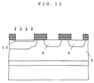
- the method of fabricating the IGBT of Fig. 10 according to the second preferred embodiment is substantially similar to the method of the first preferred embodiment described with reference to Figs. 4 to 9 except a difference in that p type impurities are implanted into the p type semiconductor region 11 between the gate electrodes 8 and annealed to partially form the p + semiconductor region 12 of higher concentration in the p type semiconductor region 11 in the process step of Fig. 11 between the process step of Fig. 7 wherein p type impurities are implanted from above the resist used in the previous process step and remaining on the gate electrodes 8 and are then annealed to form the p type base regions 4 between the gate electrodes 8 and the process step of Fig. 8 wherein the n + emitter regions 5 are formed. This results in triple diffusion of p type impurities in the p type semiconductor region 11.
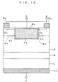
- plan structure of the third preferred embodiment is similar to that of the first preferred embodiment shown in Figs. 1 and 3.
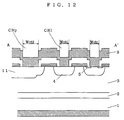
- Fig. 12 illustrates a sectional structure taken along the line A-A' of Figs. 1 and 3.
- Fig. 12 illustrates the IGBT cells described with reference to Fig. 32 which are arranged in parallel such that the emitter electrodes 9 are connected to the upper surfaces of the p type base regions 4 and n + emitter regions 5 of the respective IGBT cells through the contact holes CH 1 having the width W ch1 .
- the p type semiconductor region 11 is formed in the surface of the n - semiconductor layer 3 by double diffusion.
- the contact hole CH p having the width W ch2 greater than the width W ch1 is formed on the top surface above the p type semiconductor region 11, and the emitter electrode 9 is connected to the p type semiconductor region 11 through the contact hole CH p .
- the n + emitter regions 5 are not formed in the IGBT cell adjacent the p type semiconductor region 11.
- Like reference numerals and characters are used to designate parts identical with those of Fig. 35.
- the width W ch2 of the contact hole CH p in the p type semiconductor region 11 which is large enough to permit the hole current in the region defined by the line L 45 of Fig. 38 indicative of the spreading of the carriers to pass through completely, prevents overcurrent from concentrating on the IGBT cell adjacent the p type semiconductor region 11.
- the absence of the n + emitter regions 5 in the IGBT cell adjacent the p type semiconductor region 11 provides no parasitic thyristor consisting of the n + emitter region 5, the p type base region 4, the n - semiconductor layer 3 and the p + semiconductor layer 1. If overcurrent concentrates on the IGBT cell adjacent the p type semiconductor region 11, the IGBT breakdown due to IGBT latch-up resulting from turning on of the parasitic thyristor is prevented.
- the width W ch2 of the contact hole CH p which is large enough to meet rapid increase in hole current can remedy the situation in which part of the hole current does not completely pass through to the emitter electrodes 9 but flows into the IGBT cell adjacent the p type semiconductor region 11.
- the absence of the n + emitter regions 5 in the IGBT cell adjacent the p type semiconductor region 11 provides no parasitic thyristor consisting of the n + emitter region 5, the p type base region 4, the n - semiconductor layer 3 and the p + semiconductor layer 1. If overcurrent concentrates on the IGBT cell adjacent the p type semiconductor region 11, the IGBT breakdown due to IGBT latch-up resulting from turning on of the parasitic thyristor is prevented.
- Size reduction of the IGBT cells does not interfere with the formation of the large width W ch2 of the contact hole CH p in the p type semiconductor region 11 and the formation of the IGBT cell having no n + emitter regions 5.
- the width of the IGBT cells reduced in size is less than the thickness of the n - semiconductor layer 3 and more current flows in the contact hole CH p than in the contact hole CH 1 , reduced is the likelihood of the breakdown of the IGBT cell adjacent the p type semiconductor region 11 due to latch-up as compared with that of other IGBT cells.
- the IGBT breakdown due to IGBT latch-up resulting from turning on of the parasitic thyristor is prevented if overcurrent concentrates on the IGBT cell adjacent the p type semiconductor region 11.
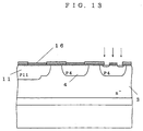
- the method of fabricating the IGBT of Fig. 12 according to the third preferred embodiment is substantially similar to the method of the first preferred embodiment described with reference to Figs. 4 to 9 except a difference in that n type impurities (e.g., arsenic) are implanted using the implantation mask 16 having a pattern which does not form the n + emitter regions 5 adjacent the p type semiconductor region 11 as shown in Fig. 13 in the process step of forming the n + emitter regions 5.
- n type impurities e.g., arsenic
- An IGBT having the advantages of both the second and third preferred embodiments is achieved by combination of the features of the second and third preferred embodiments, that is, by a structure wherein the p + semiconductor layer 12 of higher concentration than the p type semiconductor region 11 is formed partially in the surface of the p type semiconductor region 11 and the n + emitter regions 5 are not formed in the IGBT cell adjacent the p type semiconductor region 11.
- Fig. 14 is an enlarged view of a portion corresponding to the region X enclosed by the dashed-and-dotted lines of Fig. 33.
- the stripe-shaped IGBT cells each including the contact hole CH 1 having the width W ch1 are spaced the constant distance W cel from each other in parallel inside the corner portion indicated by the lines C-O-C'.
- the p type semiconductor region 11 including the stripe-shaped contact hole CH p having the width W ch2 is formed outside the corner portion indicated by the lines C-O-C'.
- Fig. 15 is a sectional view taken along the line A-A' of Fig. 14.
- Fig. 16 illustrates the basic structure of an IGBT cell according to the fifth preferred embodiment. This type of IGBT cell is generally well know in the art and is referred to as a U-shaped IGBT.
- the U-shaped IGBT cell of Fig. 16 comprises the p + semiconductor layer 1 formed of the p type semiconductor substrate and having first and second major surfaces; the n + buffer layer 2 formed on the first major surface of the p + semiconductor layer 1; the n - semiconductor layer 3 formed over the n + buffer layer 2; p type base regions 4a formed on an upper surface of the n - semiconductor layer 3 by diffusion of p type impurities; and n + emitter regions 5a formed in a partial region of the p type base regions 4a by selective diffusion of a high concentration of n type impurities.
- a groove is formed extending through the n + emitter regions 5a and p type base regions 4a into the n - semiconductor layer 3.
- a gate insulation film 7a is formed along an inner wall surface of the groove, and a gate electrode 8a made of, for example, polycrystalline silicon is buried in the interior of the gate insulation film 7a.
- the fifth preferred embodiment is similar to the first to fourth preferred embodiments in that the gate electrode 8a is formed in opposed relation to a surface of the p type base regions 4a.
- Emitter electrodes 9a made of, for example, aluminum are formed over the respective upper surfaces of the p type base regions 4a and n + emitter regions 5a.
- the gate electrode 8a and the emitter electrodes 9a are insulated from each other. Gate electrodes 8a for all IGBT cells are connected to each other, and emitter electrodes 9a for all IGBT cells are connected to each other.
- the collector electrode 10 made of, for example, aluminum is formed on the second major surface of the p + semiconductor layer 1.
- the collector electrode 10 is formed integrally for all IGBT cells.
- the U-shaped IGBT cell is further reduced in size as compared with the IGBT cells of the first to fourth preferred embodiments and is readily improved in degree of integration.
- the process steps for fabrication are simplified in the fifth preferred embodiment since the p type base region 4a should be formed entirely over the upper surface of the n - semiconductor layer 3 rather than being selectively formed.
- Fig. 15 illustrates the above stated U-shaped IGBT cells arranged in parallel such that the emitter electrodes 9a are connected to the upper surfaces of the p type base regions 4a and n + emitter regions 5a of the respective U-shaped IGBT cells through the contact holes CH 1 having the width W ch1 .
- a portion adjacent the side A of Fig. 15 represents a region outside the line C-O of the corner portion indicated by the lines C-O-C' of Fig. 14 wherein the p type semiconductor region 11 is formed in the surface of the n - semiconductor layer 3 by double diffusion in corresponding relation to the p type base region 4a of the adjacent IGBT cell and the emitter electrode 9 is connected to the upper surface of the p type semiconductor region 11 through the contact hole CH p having the width W ch2 greater than the width W ch1 of the contact hole CH 1 .
- Like reference numerals and characters are used to designate parts identical with those of Fig. 35.
- the U-shaped IGBT constructed as shown in Fig. 16 is adapted such that holes supplied from the p + semiconductor layer 1 directly below the p type semiconductor region 11 pass through the contact hole CH p having the width W ch2 in the p type semiconductor region 11 to the emitter electrodes 9a when the IGBT is on.
- the width W ch2 of the contact hole CH p in the p type semiconductor region 11 is sufficiently large, overcurrent does not concentrate on the IGBT cell adjacent the p type semiconductor region 11 to prevent the stronger likelihood of the breakdown of the IGBT cell adjacent the p type semiconductor region 11 than that of other IGBT cells due to latch-up.
- size reduction of the IGBT cells does not interfere with the large width W ch2 of the contact hole CH p in the p type semiconductor region 11.
- the width of the IGBT cells reduced in size is less than the thickness of the n - semiconductor layer 3 and more current flows in the contact hole CH p than in the contact hole CH 1 , also prevented is the stronger likelihood of the breakdown of the IGBT cell adjacent the p type semiconductor region 11 than that of other IGBT cells due to latch-up.
- Fig. 17 is an enlarged view of the region Y. Referring to Fig. 17, the gate pad GP adjacent the corner portion is formed perpendicularly to the IGBT cells, which causes the p type semiconductor region 11 to protrude to form a recessed IGBT cell region.
- This preferred embodiment provides the contact hole CH p wider than the contact hole CH 1 in the protruding p type semiconductor region 11 parallel to the IGBT cells without changing the arrangement of the IGBT cells and permits contact between the emitter electrodes 9 and the p type semiconductor region 11 through the contact hole CH p .
- the stripe-shaped IGBT cells each including the contact hole CH 1 having the width W ch1 are spaced the constant distance W cel from each other in parallel outside the corner portion indicated by the lines C-O-C'.
- the p type semiconductor region 11 including the stripe-shaped contact hole CH p having the width W ch2 is formed inside the corner portion indicated by the lines C-O-C'.
- the section taken along the line A-A' of Fig. 17 is similar to that of Fig. 15.
- this application exhibits effects when the IGBT is on, when the IGBT makes the ON-state to OFF-state transition, and when the IGBT cells are reduced in size, similar to the application of this preferred embodiment to the region X.
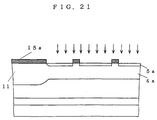
- Figs. 18 to 25 are sectional views showing process steps for fabrication of the IGBT of Fig. 15 in sequential order.
- the p + semiconductor layer 1 serving as a substrate e.g., a single crystal Si substrate
- the n + buffer layer 2 and the n - semiconductor layer 3 are sequentially formed on the first major surface of the p + semiconductor layer 1 by epitaxial growth technique.
- p type impurities e.g., boron
- p type impurities are implanted into a predetermined portion of the n - semiconductor layer 3 and are then annealed to form the p type semiconductor region 11.
- p type impurities are implanted into the entire surface of the n - semiconductor layer 3 and are then annealed to form the p type base region 4a. This results in double diffusion of p type impurities in the p type semiconductor region 11.
- n type impurities e.g., arsenic
- an implantation mask 15a having a desired pattern and are then annealed to form the n + emitter regions 5a.
- selective silicon etching is performed on the n + emitter regions 5a, the p type base region 4a, and the n - semiconductor layer 3 by means of RIE (reactive ion etching) technique to form stripe-shaped grooves in desired positions.
- RIE reactive ion etching
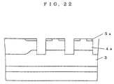
- the gate insulation film 7a such as a thermal oxidation film is formed over the upper surfaces of the p type semiconductor region 11 and n + emitter regions 5a and the inner surfaces of the grooves formed in the foregoing process step.
- Doped polysilicon is deposited on the gate insulation film 7a so as to be buried in the grooves formed in the foregoing process step to form the gate electrode 8a.
- the gate insulating film 7a is selectively etched, and the layer insulation films 13 made of, for example, PSG (phospho-silicate glass) are formed on the gate electrodes 8a and the remaining gate insulating films 7a.
- the emitter electrodes 9a made of, for example, aluminum are formed over the upper surfaces of the p type base regions 4a and n + emitter regions 5a between the layer insulation films 13. Emitter electrodes 9a for all IGBT cells are connected to each other.
- the collector electrode 10 made of, for example, aluminum is formed over the second major surface of the p + semiconductor layer 1 integrally for all IGBT cells. This completes the IGBT of Fig. 15.
- plan structure of the sixth preferred embodiment is similar to that of the fifth preferred embodiment shown in Figs. 14 and 17.
- Fig. 26 illustrates a sectional structure taken along the line A-A' of Figs. 14 and 17.
- Fig. 26 illustrates the U-shaped IGBT cells described with reference to Fig. 16 which are arranged in parallel such that the emitter electrodes 9a are connected to the upper surfaces of the p type base regions 4a and n + emitter regions 5a of the respective IGBT cells through the contact holes CH 1 having the width W ch1 .
- the p type semiconductor region 11 is formed in the surface of the n - semiconductor layer 3 by double diffusion in corresponding relation to the p type base regions 4 of the IGBT cells, and a p + semiconductor layer 12a having a higher concentration than that of the p type semiconductor region 11 is formed partially in a surface of the p type semiconductor region 11.
- the contact hole CH p having the width W ch2 greater than the width W ch1 of the contact holes CH 1 is formed on the top surface above the p + semiconductor layer 12a, and the emitter electrode 9a is connected to the p + semiconductor layer 12a through the contact hole CH p .
- Like reference numerals and characters are used to designate parts identical with those of Fig. 35.
- the contact resistance between the emitter electrode 9a to and the p + semiconductor layer 12a is decreased to promote a hole current flow by providing the sufficiently large width W ch2 of the contact hole CH p in the p type semiconductor region 11 and the p + semiconductor layer 12a of higher concentration than the p type semiconductor region 11 in the portion corresponding to the contact hole CH p of the p type semiconductor region 11. This prevents overcurrent from concentrating on the IGBT cell adjacent the p type semiconductor region 11 to prevent the stronger likelihood of the breakdown of the IGBT cell adjacent the p type semiconductor region 11 than that of other IGBT cells due to latch-up.
- the contact resistance between the emitter electrode 9 and the p + semiconductor layer 12a is decreased to promote the hole current flow by providing the width W ch2 of the contact hole CH p which is large enough to meet rapid increase in hole current and by providing the p + semiconductor layer 12a of higher concentration than the p type semiconductor region 11 and formed partially in the portion corresponding to the contact hole CH p of the p type semiconductor region 11.
- This can remedy the situation in which part of the hole current does not completely pass through to the emitter electrodes 9a but flows into the IGBT cell adjacent the p type semiconductor region 11. Also prevented is the stronger likelihood of the breakdown of the IGBT cell adjacent the p type semiconductor region 11 than that of other IGBT cells due to latch-up.
- Size reduction of the IGBT cells does not interfere with the formation of the p + semiconductor region 12a of higher concentration than the p type semiconductor region 11 in the surface of the p type semiconductor region 11 and the formation of the large width W ch2 of the contact hole CH p .
- the width of the IGBT cells reduced in size is less than the thickness of the n - semiconductor layer 3 and more current flows in the contact hole CH p than in the contact hole CH 1 , also prevented is the stronger likelihood of the breakdown of the IGBT cell adjacent the p type semiconductor region 11 than that of other IGBT cells due to latch-up.
- the method of fabricating the IGBT of Fig. 26 according to the sixth preferred embodiment is substantially similar to the method of the fifth preferred embodiment described with reference to Figs. 18 to 25 except a difference in that p type impurities are implanted into the p type semiconductor region 11 in a predetermined position and annealed to partially form the p + semiconductor region 12a of higher concentration in the p type semiconductor region 11 by using the mask 15a in the process step of Fig. 27 between the process step of implanting n type impurities (e.g., arsenic) into the predetermined portion of the p type base region 4a and annealing the n type impurities to form the n + emitter regions 5a and the next process step of forming the stripe-shaped grooves.
- n type impurities e.g., arsenic
- plan structure of the seventh preferred embodiment is similar to that of the fifth preferred embodiment shown in Figs. 14 and 17.
- Fig. 28 illustrates a sectional structure taken along the line A-A' of Figs. 14 and 17.
- Fig. 28 illustrates the IGBT cells described with reference to Fig. 16 which are arranged in parallel such that the emitter electrodes 9a are connected to the upper surfaces of the p type base regions 4a and n + emitter regions 5a of the respective IGBT cells through the contact holes CH 1 having the width W ch1 .
- the p type semiconductor region 11 is formed in the surface of the n - semiconductor layer 3 by double diffusion.
- the contact hole CH p having the width W ch2 greater than the width W ch1 of the contact holes CH 1 is formed on the top surface above the p type semiconductor region 11, and the emitter electrode 9a is connected to the p type semiconductor region 11 through the contact hole CH p .
- the n + emitter regions 5a are not formed in the IGBT cell adjacent the p type semiconductor region 11.
- Like reference numerals and characters are used to designate parts identical with those of Fig. 35.
- the sufficiently large width W ch2 of the contact hole CH p in the p type semiconductor region 11 prevents overcurrent from concentrating on the IGBT cell adjacent the p type semiconductor region 11. Further, the absence of the n + emitter regions 5a in the IGBT cell adjacent the p type semiconductor region 11 provides no parasitic thyristor consisting of the n + emitter region 5a, the p type base region 4a, the n - semiconductor layer 3 and the p + semiconductor layer 1. If overcurrent concentrates on the IGBT cell adjacent the p type semiconductor region 11, the IGBT breakdown due to IGBT latch-up resulting from turning on of the parasitic thyristor is prevented.
- the width W ch2 of the contact hole CH p which is large enough to meet rapid increase in hole current can remedy the situation in which part of the hole current does not completely pass through to the emitter electrodes 9a but flows into the IGBT cell adjacent the p type semiconductor region 11.
- the absence of the n + emitter regions 5a in the IGBT cell adjacent the p type semiconductor region 11 and in the IGBT cell adjacent the foregoing IGBT cell provides no parasitic thyristor consisting of the n + emitter region 5a, the p type base region 4a, the n - semiconductor layer 3 and the p + semiconductor layer 1. If overcurrent concentrates on the IGBT cell adjacent the p type semiconductor region 11, the IGBT breakdown due to IGBT latch-up resulting from turning on of the parasitic thyristor is prevented.
- Size reduction of the IGBT cells does not interfere with the formation of the large width W ch2 of the contact hole CH p in the p type semiconductor region 11 and the formation of the IGBT cell having no n + emitter regions 5a.
- the width of the IGBT cells reduced in size is less than the thickness of the n - semiconductor layer 3 and more current flows in the contact hole CH p than in the contact hole CH 1 , reduced is the likelihood of the breakdown of the IGBT cell adjacent the p type semiconductor region 11 due to latch-up as compared with that of other IGBT cells. If overcurrent concentrates on the IGBT cell adjacent the p type semiconductor region 11, the IGBT breakdown due to IGBT latch-up resulting from turning on of the parasitic thyristor is prevented.
- the method of fabricating the IGBT of Fig. 28 according to the seventh preferred embodiment is substantially similar to the method of the fifth preferred embodiment described with reference to Figs. 18 to 25 except a difference in that n type impurities (e.g., arsenic) are implanted using an implantation mask 16 having a pattern which does not form the n + emitter regions 5a adjacent the p type semiconductor region 11 as shown in Fig. 29 in the process step of forming the n + emitter regions 5a.
- n type impurities e.g., arsenic
- An IGBT having the advantages of both the sixth and seventh preferred embodiments is achieved by combination of the features of the sixth and seventh preferred embodiments, that is, by a structure wherein the p + semiconductor layer 12a of higher concentration than the p type semiconductor region 11 is formed partially in the surface of the p type semiconductor region 11 and the n + emitter regions 5a are not formed in the IGBT cell adjacent the p type semiconductor region 11.
- the above stated insulated gate semiconductor device and the method of fabricating the same according to present invention are applied to the IGBTs in the first to eighth preferred embodiments.
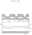
- the present invention may be applied similarly to an EST (emitter switched thyristor) as shown in Fig. 30.
- Fig. 30 is a view corresponding to Fig. 2 employed in the first preferred embodiment. Like reference numerals are used to designate parts identical with those of Fig. 2.
- the structure of Fig. 30 differs from that of Fig. 2 in that the n + emitter regions 5 between the gate electrodes 8 are joined together in every other IGBT cell.
- the structures similar to those of the first to sixth preferred embodiments provide similar effects.
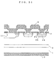
- the insulated gate semiconductor device and the method of fabricating the same of the first to eighth preferred embodiments according to the present invention may be applied similarly to an MCT (MOS controlled thyristor) as shown in Fig. 31.
- MCT MOS controlled thyristor
- Fig. 31 is a view corresponding to Fig. 2 employed in the first preferred embodiment. Like reference numerals and characters are used to designate parts identical with those of Fig. 2.
- the structure of Fig. 31 differs from that of Fig. 2 in that it comprises p type base regions 4b between the gate electrodes 8, n type semiconductor regions 14 in the respective p type base regions 4b between the gate electrodes 8, and p + emitter regions 5b in the n type semiconductor regions 14 in place of the n + emitter regions 5, to provide a vertical triple diffusion structure.
- the structures similar to those of the first to sixth preferred embodiments provide similar effects.
Landscapes
- Thyristors (AREA)
- Metal-Oxide And Bipolar Metal-Oxide Semiconductor Integrated Circuits (AREA)
Applications Claiming Priority (3)
| Application Number | Priority Date | Filing Date | Title |
|---|---|---|---|
| JP5276876A JP2987040B2 (ja) | 1993-11-05 | 1993-11-05 | 絶縁ゲート型半導体装置 |
| JP27687693 | 1993-11-05 | ||
| EP94116733A EP0652597A1 (fr) | 1993-11-05 | 1994-10-24 | Dispositif semiconducteur à grille isolée et procédé pour sa fabrication |
Related Parent Applications (2)
| Application Number | Title | Priority Date | Filing Date |
|---|---|---|---|
| EP94116733.0 Division | 1994-10-24 | ||
| EP94116733A Division EP0652597A1 (fr) | 1993-11-05 | 1994-10-24 | Dispositif semiconducteur à grille isolée et procédé pour sa fabrication |
Publications (2)
| Publication Number | Publication Date |
|---|---|
| EP1376703A2 true EP1376703A2 (fr) | 2004-01-02 |
| EP1376703A3 EP1376703A3 (fr) | 2008-01-09 |
Family
ID=17575638
Family Applications (2)
| Application Number | Title | Priority Date | Filing Date |
|---|---|---|---|
| EP01126332A Withdrawn EP1376703A3 (fr) | 1993-11-05 | 1994-10-24 | Dispositif semi-conducteur à grille isolée et sa méthode de fabrication |
| EP94116733A Ceased EP0652597A1 (fr) | 1993-11-05 | 1994-10-24 | Dispositif semiconducteur à grille isolée et procédé pour sa fabrication |
Family Applications After (1)
| Application Number | Title | Priority Date | Filing Date |
|---|---|---|---|
| EP94116733A Ceased EP0652597A1 (fr) | 1993-11-05 | 1994-10-24 | Dispositif semiconducteur à grille isolée et procédé pour sa fabrication |
Country Status (3)
| Country | Link |
|---|---|
| US (2) | US5525816A (fr) |
| EP (2) | EP1376703A3 (fr) |
| JP (1) | JP2987040B2 (fr) |
Families Citing this family (15)
| Publication number | Priority date | Publication date | Assignee | Title |
|---|---|---|---|---|
| JP3410286B2 (ja) | 1996-04-01 | 2003-05-26 | 三菱電機株式会社 | 絶縁ゲート型半導体装置 |
| EP1009035B1 (fr) * | 1997-08-29 | 2004-07-21 | Mitsubishi Denki Kabushiki Kaisha | Dispositif a semi-conducteur a grille isolee et procede de fabrication |
| EP1060517A1 (fr) | 1998-02-27 | 2000-12-20 | ABB Semiconductors AG | Transistor bipolaire avec electrode de grille isolee |
| DE19823170A1 (de) * | 1998-05-23 | 1999-11-25 | Asea Brown Boveri | Bipolartransistor mit isolierter Gateelektrode |
| JP4852188B2 (ja) * | 1999-12-06 | 2012-01-11 | 株式会社豊田中央研究所 | 半導体装置 |
| US6635926B2 (en) * | 2000-08-30 | 2003-10-21 | Shindengen Electric Manufacturing Co., Ltd. | Field effect transistor with high withstand voltage and low resistance |
| US6777783B2 (en) * | 2001-12-26 | 2004-08-17 | Kabushiki Kaisha Toshiba | Insulated gate bipolar transistor |
| JP3931138B2 (ja) * | 2002-12-25 | 2007-06-13 | 三菱電機株式会社 | 電力用半導体装置及び電力用半導体装置の製造方法 |
| US7157785B2 (en) * | 2003-08-29 | 2007-01-02 | Fuji Electric Device Technology Co., Ltd. | Semiconductor device, the method of manufacturing the same, and two-way switching device using the semiconductor devices |
| DE102005053487B4 (de) * | 2005-11-09 | 2011-06-09 | Infineon Technologies Ag | Leistungs-IGBT mit erhöhter Robustheit |
| JP5047805B2 (ja) | 2005-11-22 | 2012-10-10 | 新電元工業株式会社 | トレンチゲートパワー半導体装置 |
| JP4630862B2 (ja) * | 2006-12-22 | 2011-02-09 | 株式会社東芝 | 半導体装置 |
| JP5512455B2 (ja) * | 2010-08-02 | 2014-06-04 | 株式会社東芝 | 半導体装置 |
| KR101955055B1 (ko) | 2014-11-28 | 2019-03-07 | 매그나칩 반도체 유한회사 | 전력용 반도체 소자 및 그 소자의 제조 방법 |
| US11222858B1 (en) * | 2020-06-19 | 2022-01-11 | Alpha And Omega Semiconductor International Lp | Semiconductor package having enlarged gate pad and method of making the same |
Family Cites Families (10)
| Publication number | Priority date | Publication date | Assignee | Title |
|---|---|---|---|---|
| JPH0752770B2 (ja) * | 1985-09-30 | 1995-06-05 | 株式会社東芝 | 導電変調型mosfet |
| JPH02312280A (ja) * | 1989-05-26 | 1990-12-27 | Mitsubishi Electric Corp | 絶縁ゲート型バイポーラトランジスタ |
| US5208471A (en) * | 1989-06-12 | 1993-05-04 | Hitachi, Ltd. | Semiconductor device and manufacturing method therefor |
| US5119153A (en) * | 1989-09-05 | 1992-06-02 | General Electric Company | Small cell low contact resistance rugged power field effect devices and method of fabrication |
| JPH0396282A (ja) * | 1989-09-08 | 1991-04-22 | Fuji Electric Co Ltd | 絶縁ゲート型半導体装置 |
| US5076766A (en) * | 1989-12-12 | 1991-12-31 | Allied-Signal Inc. | Turbocharger bearing retention and lubrication system |
| JP2858404B2 (ja) * | 1990-06-08 | 1999-02-17 | 株式会社デンソー | 絶縁ゲート型バイポーラトランジスタおよびその製造方法 |
| JP2504862B2 (ja) * | 1990-10-08 | 1996-06-05 | 三菱電機株式会社 | 半導体装置及びその製造方法 |
| US5324966A (en) * | 1992-04-07 | 1994-06-28 | Toyo Denki Seizo Kabushiki Kaisha | MOS-controlled thyristor |
| US5357120A (en) * | 1992-07-14 | 1994-10-18 | Hitachi Ltd. | Compound semiconductor device and electric power converting apparatus using such device |
-
1993
- 1993-11-05 JP JP5276876A patent/JP2987040B2/ja not_active Expired - Lifetime
-
1994
- 1994-10-21 US US08/327,368 patent/US5525816A/en not_active Ceased
- 1994-10-24 EP EP01126332A patent/EP1376703A3/fr not_active Withdrawn
- 1994-10-24 EP EP94116733A patent/EP0652597A1/fr not_active Ceased
-
1997
- 1997-10-10 US US08/948,298 patent/USRE36818E/en not_active Expired - Lifetime
Also Published As
| Publication number | Publication date |
|---|---|
| US5525816A (en) | 1996-06-11 |
| JP2987040B2 (ja) | 1999-12-06 |
| USRE36818E (en) | 2000-08-15 |
| EP1376703A3 (fr) | 2008-01-09 |
| JPH07131012A (ja) | 1995-05-19 |
| EP0652597A1 (fr) | 1995-05-10 |
Similar Documents
| Publication | Publication Date | Title |
|---|---|---|
| EP1158582B1 (fr) | Diode de type pin. | |
| USRE38953E1 (en) | Insulated gate semiconductor device and method of manufacturing the same | |
| KR100290693B1 (ko) | 전계 효과에 의해 제어 가능한 파워 반도체 소자 | |
| US6051850A (en) | Insulated gate bipolar junction transistors having built-in freewheeling diodes therein | |
| EP0594049B1 (fr) | Transistor bipolaire à grille isolée et méthode de fabrication correspondante | |
| CN1967868B (zh) | 半导体装置及其制造方法 | |
| EP0732749B1 (fr) | Dispositif semi-conducteur bipolaire à grille isolée et méthode de fabrication | |
| US5891776A (en) | Methods of forming insulated-gate semiconductor devices using self-aligned trench sidewall diffusion techniques | |
| US5289019A (en) | Insulated gate bipolar transistor | |
| US5464992A (en) | Insulated gate bipolar transistor provided with a minority carrier extracting layer | |
| US5525816A (en) | Insulated gate semiconductor device with stripe widths | |
| JP2005505921A (ja) | フローティングアイランド電圧維持層を有する半導体パワーデバイス | |
| US5173435A (en) | Insulated gate bipolar transistor | |
| US11393901B2 (en) | Cell layouts for MOS-gated devices for improved forward voltage | |
| EP0564094B1 (fr) | Diode à grille et méthode pour sa fabrication | |
| US5414290A (en) | IGBT with self-aligning cathode pattern and method for producing it | |
| US5861638A (en) | Insulated gate bipolar transistor | |
| EP0615292A1 (fr) | Transistor bipolaire à grille isolée | |
| KR0146640B1 (ko) | 전압구동형 사이리스터와 그 제조방법 | |
| WO2000010204A1 (fr) | Dispositif semi-conducteur a grille en tranchee | |
| US5981983A (en) | High voltage semiconductor device | |
| US7741655B2 (en) | Semiconductor device | |
| JP3657938B2 (ja) | 半導体装置 | |
| KR100277680B1 (ko) | 개선된 엘아이지비티 전력소자 | |
| JPH0846192A (ja) | 半導体装置 |
Legal Events
| Date | Code | Title | Description |
|---|---|---|---|
| PUAI | Public reference made under article 153(3) epc to a published international application that has entered the european phase |
Free format text: ORIGINAL CODE: 0009012 |
|
| 17P | Request for examination filed |
Effective date: 20011106 |
|
| AC | Divisional application: reference to earlier application |
Ref document number: 0652597 Country of ref document: EP Kind code of ref document: P |
|
| AK | Designated contracting states |
Kind code of ref document: A2 Designated state(s): DE FR GB |
|
| RAP1 | Party data changed (applicant data changed or rights of an application transferred) |
Owner name: MITSUBISHI DENKI KABUSHIKI KAISHA |
|
| PUAL | Search report despatched |
Free format text: ORIGINAL CODE: 0009013 |
|
| AK | Designated contracting states |
Kind code of ref document: A3 Designated state(s): DE FR GB |
|
| RIC1 | Information provided on ipc code assigned before grant |
Ipc: H01L 21/331 20060101ALI20071205BHEP Ipc: H01L 29/417 20060101ALI20071205BHEP Ipc: H01L 29/10 20060101ALI20071205BHEP Ipc: H01L 29/749 20060101ALI20071205BHEP Ipc: H01L 29/739 20060101AFI20031110BHEP Ipc: H01L 29/745 20060101ALI20071205BHEP |
|
| AKX | Designation fees paid |
Designated state(s): DE FR GB |
|
| 17Q | First examination report despatched |
Effective date: 20090202 |
|
| STAA | Information on the status of an ep patent application or granted ep patent |
Free format text: STATUS: THE APPLICATION IS DEEMED TO BE WITHDRAWN |
|
| 18D | Application deemed to be withdrawn |
Effective date: 20090613 |