EP1377144A2 - Procédé de montage et structure d'un boîtier de type sans fils - Google Patents
Procédé de montage et structure d'un boîtier de type sans fils Download PDFInfo
- Publication number
- EP1377144A2 EP1377144A2 EP03076653A EP03076653A EP1377144A2 EP 1377144 A2 EP1377144 A2 EP 1377144A2 EP 03076653 A EP03076653 A EP 03076653A EP 03076653 A EP03076653 A EP 03076653A EP 1377144 A2 EP1377144 A2 EP 1377144A2
- Authority
- EP
- European Patent Office
- Prior art keywords
- substrate
- solder
- thermal pad
- solder mask
- package
- Prior art date
- Legal status (The legal status is an assumption and is not a legal conclusion. Google has not performed a legal analysis and makes no representation as to the accuracy of the status listed.)
- Withdrawn
Links
Images

Classifications
-
- H—ELECTRICITY
- H10—SEMICONDUCTOR DEVICES; ELECTRIC SOLID-STATE DEVICES NOT OTHERWISE PROVIDED FOR
- H10W—GENERIC PACKAGES, INTERCONNECTIONS, CONNECTORS OR OTHER CONSTRUCTIONAL DETAILS OF DEVICES COVERED BY CLASS H10
- H10W70/00—Package substrates; Interposers; Redistribution layers [RDL]
- H10W70/60—Insulating or insulated package substrates; Interposers; Redistribution layers
-
- H—ELECTRICITY
- H05—ELECTRIC TECHNIQUES NOT OTHERWISE PROVIDED FOR
- H05K—PRINTED CIRCUITS; CASINGS OR CONSTRUCTIONAL DETAILS OF ELECTRIC APPARATUS; MANUFACTURE OF ASSEMBLAGES OF ELECTRICAL COMPONENTS
- H05K1/00—Printed circuits
- H05K1/02—Details
- H05K1/0201—Thermal arrangements, e.g. for cooling, heating or preventing overheating
- H05K1/0203—Cooling of mounted components
- H05K1/0204—Cooling of mounted components using means for thermal conduction connection in the thickness direction of the substrate
- H05K1/0206—Cooling of mounted components using means for thermal conduction connection in the thickness direction of the substrate by printed thermal vias
-
- H—ELECTRICITY
- H05—ELECTRIC TECHNIQUES NOT OTHERWISE PROVIDED FOR
- H05K—PRINTED CIRCUITS; CASINGS OR CONSTRUCTIONAL DETAILS OF ELECTRIC APPARATUS; MANUFACTURE OF ASSEMBLAGES OF ELECTRICAL COMPONENTS
- H05K3/00—Apparatus or processes for manufacturing printed circuits
- H05K3/30—Assembling printed circuits with electric components, e.g. with resistors
- H05K3/32—Assembling printed circuits with electric components, e.g. with resistors electrically connecting electric components or wires to printed circuits
- H05K3/34—Assembling printed circuits with electric components, e.g. with resistors electrically connecting electric components or wires to printed circuits by soldering
- H05K3/341—Surface mounted components
-
- H—ELECTRICITY
- H05—ELECTRIC TECHNIQUES NOT OTHERWISE PROVIDED FOR
- H05K—PRINTED CIRCUITS; CASINGS OR CONSTRUCTIONAL DETAILS OF ELECTRIC APPARATUS; MANUFACTURE OF ASSEMBLAGES OF ELECTRICAL COMPONENTS
- H05K3/00—Apparatus or processes for manufacturing printed circuits
- H05K3/30—Assembling printed circuits with electric components, e.g. with resistors
- H05K3/32—Assembling printed circuits with electric components, e.g. with resistors electrically connecting electric components or wires to printed circuits
- H05K3/34—Assembling printed circuits with electric components, e.g. with resistors electrically connecting electric components or wires to printed circuits by soldering
- H05K3/3452—Solder masks
-
- H—ELECTRICITY
- H10—SEMICONDUCTOR DEVICES; ELECTRIC SOLID-STATE DEVICES NOT OTHERWISE PROVIDED FOR
- H10W—GENERIC PACKAGES, INTERCONNECTIONS, CONNECTORS OR OTHER CONSTRUCTIONAL DETAILS OF DEVICES COVERED BY CLASS H10
- H10W40/00—Arrangements for thermal protection or thermal control
- H10W40/20—Arrangements for cooling
- H10W40/22—Arrangements for cooling characterised by their shape, e.g. having conical or cylindrical projections
- H10W40/226—Arrangements for cooling characterised by their shape, e.g. having conical or cylindrical projections characterised by projecting parts, e.g. fins to increase surface area
- H10W40/228—Arrangements for cooling characterised by their shape, e.g. having conical or cylindrical projections characterised by projecting parts, e.g. fins to increase surface area the projecting parts being wire-shaped or pin-shaped
-
- H—ELECTRICITY
- H05—ELECTRIC TECHNIQUES NOT OTHERWISE PROVIDED FOR
- H05K—PRINTED CIRCUITS; CASINGS OR CONSTRUCTIONAL DETAILS OF ELECTRIC APPARATUS; MANUFACTURE OF ASSEMBLAGES OF ELECTRICAL COMPONENTS
- H05K2201/00—Indexing scheme relating to printed circuits covered by H05K1/00
- H05K2201/09—Shape and layout
- H05K2201/09818—Shape or layout details not covered by a single group of H05K2201/09009 - H05K2201/09809
- H05K2201/099—Coating over pads, e.g. solder resist partly over pads
-
- H—ELECTRICITY
- H05—ELECTRIC TECHNIQUES NOT OTHERWISE PROVIDED FOR
- H05K—PRINTED CIRCUITS; CASINGS OR CONSTRUCTIONAL DETAILS OF ELECTRIC APPARATUS; MANUFACTURE OF ASSEMBLAGES OF ELECTRICAL COMPONENTS
- H05K2201/00—Indexing scheme relating to printed circuits covered by H05K1/00
- H05K2201/10—Details of components or other objects attached to or integrated in a printed circuit board
- H05K2201/10613—Details of electrical connections of non-printed components, e.g. special leads
- H05K2201/10621—Components characterised by their electrical contacts
- H05K2201/10727—Leadless chip carrier [LCC], e.g. chip-modules for cards
-
- H—ELECTRICITY
- H05—ELECTRIC TECHNIQUES NOT OTHERWISE PROVIDED FOR
- H05K—PRINTED CIRCUITS; CASINGS OR CONSTRUCTIONAL DETAILS OF ELECTRIC APPARATUS; MANUFACTURE OF ASSEMBLAGES OF ELECTRICAL COMPONENTS
- H05K2201/00—Indexing scheme relating to printed circuits covered by H05K1/00
- H05K2201/10—Details of components or other objects attached to or integrated in a printed circuit board
- H05K2201/10613—Details of electrical connections of non-printed components, e.g. special leads
- H05K2201/10954—Other details of electrical connections
- H05K2201/10969—Metallic case or integral heatsink of component electrically connected to a pad on PCB
-
- H—ELECTRICITY
- H05—ELECTRIC TECHNIQUES NOT OTHERWISE PROVIDED FOR
- H05K—PRINTED CIRCUITS; CASINGS OR CONSTRUCTIONAL DETAILS OF ELECTRIC APPARATUS; MANUFACTURE OF ASSEMBLAGES OF ELECTRICAL COMPONENTS
- H05K2203/00—Indexing scheme relating to apparatus or processes for manufacturing printed circuits covered by H05K3/00
- H05K2203/04—Soldering or other types of metallurgic bonding
- H05K2203/0455—PTH for surface mount device [SMD], e.g. wherein solder flows through the PTH during mounting
-
- H—ELECTRICITY
- H05—ELECTRIC TECHNIQUES NOT OTHERWISE PROVIDED FOR
- H05K—PRINTED CIRCUITS; CASINGS OR CONSTRUCTIONAL DETAILS OF ELECTRIC APPARATUS; MANUFACTURE OF ASSEMBLAGES OF ELECTRICAL COMPONENTS
- H05K2203/00—Indexing scheme relating to apparatus or processes for manufacturing printed circuits covered by H05K3/00
- H05K2203/11—Treatments characterised by their effect, e.g. heating, cooling, roughening
- H05K2203/1178—Means for venting or for letting gases escape
-
- H—ELECTRICITY
- H05—ELECTRIC TECHNIQUES NOT OTHERWISE PROVIDED FOR
- H05K—PRINTED CIRCUITS; CASINGS OR CONSTRUCTIONAL DETAILS OF ELECTRIC APPARATUS; MANUFACTURE OF ASSEMBLAGES OF ELECTRICAL COMPONENTS
- H05K3/00—Apparatus or processes for manufacturing printed circuits
- H05K3/0094—Filling or covering plated through-holes or blind plated vias, e.g. for masking or for mechanical reinforcement
-
- H—ELECTRICITY
- H05—ELECTRIC TECHNIQUES NOT OTHERWISE PROVIDED FOR
- H05K—PRINTED CIRCUITS; CASINGS OR CONSTRUCTIONAL DETAILS OF ELECTRIC APPARATUS; MANUFACTURE OF ASSEMBLAGES OF ELECTRICAL COMPONENTS
- H05K3/00—Apparatus or processes for manufacturing printed circuits
- H05K3/40—Forming printed elements for providing electric connections to or between printed circuits
- H05K3/42—Plated through-holes or plated via connections
-
- H—ELECTRICITY
- H10—SEMICONDUCTOR DEVICES; ELECTRIC SOLID-STATE DEVICES NOT OTHERWISE PROVIDED FOR
- H10W—GENERIC PACKAGES, INTERCONNECTIONS, CONNECTORS OR OTHER CONSTRUCTIONAL DETAILS OF DEVICES COVERED BY CLASS H10
- H10W74/00—Encapsulations, e.g. protective coatings
-
- H—ELECTRICITY
- H10—SEMICONDUCTOR DEVICES; ELECTRIC SOLID-STATE DEVICES NOT OTHERWISE PROVIDED FOR
- H10W—GENERIC PACKAGES, INTERCONNECTIONS, CONNECTORS OR OTHER CONSTRUCTIONAL DETAILS OF DEVICES COVERED BY CLASS H10
- H10W90/00—Package configurations
- H10W90/701—Package configurations characterised by the relative positions of pads or connectors relative to package parts
- H10W90/751—Package configurations characterised by the relative positions of pads or connectors relative to package parts of bond wires
- H10W90/756—Package configurations characterised by the relative positions of pads or connectors relative to package parts of bond wires between a chip and a stacked lead frame, conducting package substrate or heat sink
-
- Y—GENERAL TAGGING OF NEW TECHNOLOGICAL DEVELOPMENTS; GENERAL TAGGING OF CROSS-SECTIONAL TECHNOLOGIES SPANNING OVER SEVERAL SECTIONS OF THE IPC; TECHNICAL SUBJECTS COVERED BY FORMER USPC CROSS-REFERENCE ART COLLECTIONS [XRACs] AND DIGESTS
- Y02—TECHNOLOGIES OR APPLICATIONS FOR MITIGATION OR ADAPTATION AGAINST CLIMATE CHANGE
- Y02P—CLIMATE CHANGE MITIGATION TECHNOLOGIES IN THE PRODUCTION OR PROCESSING OF GOODS
- Y02P70/00—Climate change mitigation technologies in the production process for final industrial or consumer products
- Y02P70/50—Manufacturing or production processes characterised by the final manufactured product
Definitions
- the present invention generally relates to semiconductor integrated circuit (IC) devices. More particularly, this invention relates to a method and structure for solder-mounting a leadless IC package to a substrate equipped with thermal vias, and for preventing solder from entering the vias during solder reflow.
- IC semiconductor integrated circuit
- Various packaging configurations have been proposed for mounting IC devices to circuit boards and other electronic substrates.
- Conventional packages typically require wire leads that electrically connect the package to contact pads on the surface of the circuit board.
- Leadless packages have been developed that do not have wire leads, but instead have input/output (I/O) pads exposed at a surface of the package.
- Such packages are known in the industry as quad flat non-leaded (QFN) packages.
- QFN quad flat non-leaded
- An example is a QFN package commercially available from Amkor Technology under the name Microleadframe (MLF).
- MLF Microleadframe
- the Amkor MLF package is a plastic-encapsulated IC package 30 with a copper leadframe 46 that defines lands (I/O pads) 40 near the outer perimeter of the package 30.
- An IC device 42 is attached to a die paddle (thermal pad) 32 located on the same surface of the package 30 as the pads 40 and surrounded by the pads 40.
- Wire leads 44 electrically connect the IC device 42 to the I/O pads 40, which in turn are electrically and mechanically connected with solder joints to contact pads on a circuit board or other suitable substrate.
- the thermal pad 32 promotes heat transfer from the IC device 42 to the circuit board.
- the circuit board can be equipped with a thermal pad on its surface for contact with the thermal pad 32 of the package 30 to promote heat transfer and dissipation in the circuit board.
- Heat transfer is promoted by soldering the thermal pad 32 to the thermal pad of the circuit board, and further by forming plated vias (plated through-holes, or PTH's) in the thermal pad of the circuit board to promote heat transfer through the circuit board to the surface opposite the package 30, where a heat sink or other suitable means can be provided for dissipating heat.
- plated vias plated through-holes, or PTH's
- solder joints at the I/O pads of a leadless package must be sufficiently thick (in the direction normal to the pads) to be compliant for surviving numerous thermal cycles. Solder joint height at the pads is affected by the relatively large volume of solder present between the thermal pads of the package and circuit board. If thermal vias are present in the thermal pad of the circuit board, loss of solder through the vias during reflow can cause the package to collapse toward the circuit board, reducing solder joint height.
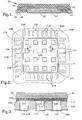
- Figures 2 through 4 show a solution proposed in the past to prevent solder wicking into thermal vias.
- Figure 2 represents the surface of a substrate 112 prepared for mounting a leadless package, e.g., the package 30 of Figure 1.
- the substrate 112 is shown as having a thermal pad 114 surrounded by input/output pads 116, and with plated thermal vias 118 in the thermal pad 114 and extending through the substrate 112.
- a solder mask is shown as having been applied to the surface of the substrate 112, with openings 124 and 126 patterned in the solder mask to define an outer mask portion 120 surrounding the thermal pad 114 and interior mask portions 122 covering each of the vias 118, thereby plugging or "tenting" the vias 118.
- solder paste 134 is then applied to the thermal pad 114, and the leadless package 30 is placed on the substrate 112 so that its thermal pad 32 is registered with the solder paste 134.
- Solder paste is also deposited on the contact pads 116 (shown in Figure 2) at the same time as the paste 134 is deposited on the thermal pad 114, such that the I/O pads 40 of the package 30 also register with solder paste.
- the solder paste 134 is then reflowed to form a solder joint 136 between the thermal pads 114 and 32, as depicted in Figure 4, as well as solder joints that electrically connect the I/O pads 40 to the contact pads 116.
- Figures 3 and 4 show the vias 118 as also being closed by solder masks 128 applied to the lower surface of the substrate 112. In practice, only one of the sets of solder masks 122 or 128 would typically be used to plug the vias 118. Reported experiments suggest that masking the vias 118 at the surface of the thermal pad 114 (with solder masks 122) provides better results in terms of reducing void formation during reflow.
- the present invention is directed to a method and circuit structure for mounting a leadless IC device to a substrate, such as a circuit board.
- the method and structure are directed to mounting a leadless device to a substrate having a thermal pad on a first surface thereof, a plurality of contact pads surrounding the thermal pad, and one or more plated vias in the thermal pad and extending through the substrate to an oppositely-disposed second surface of the substrate.
- the leadless device comprises a thermal pad disposed at a surface of the leadless device for alignment with the substrate thermal pad, a plurality of input/output pads surrounding the device thermal pad for alignment with the contact pads of the substrate, and an integrated circuit device electrically connected to the input/output pads.
- solder mask is provided on the first surface of the substrate, at least a portion of which is deposited on the substrate thermal pad and surrounds the plated via but does not block the plated via. In this manner, the portion of the solder mask defines a barrier between the solder and the plated via, but allows for outgassing through the via during the reflow process.
- the present invention provides a solution to the problem of solder wicking through thermal vias during reflow, without resorting to blocking the vias as was believed necessary in the past.
- solder joints having adequate thicknesses can be readily achieved, promoting the reliability of the leadless device.
- An added benefit is the reduction in voids within the solder joint between the thermal pads of the leadless device and substrate as a result of the vias enabling flux outgassing during solder reflow.
- the solder mask remains as a permanent structure between the leadless device and the substrate, and can be selectively applied to closely surround the perimeters of the individual vias so that the remaining surface of the substrate thermal pad is exposed for attachment with solder to the leadless device.
- the solder mask can also be patterned to define a grid through which limited surface regions of the substrate thermal pad are exposed, creating multiple solder joints defined between the thermal pads of the leadless device and substrate.
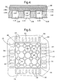
- Figure 5 represents a circuit structure 10 in accordance with a preferred embodiment of this invention.
- Figure 5 shows a surface of a substrate 12 prepared for mounting a leadless package, represented as the MLF package 30 of Figure 1, and is therefore similar in appearance to the substrate surface depicted in Figure 2.
- the substrate 12 could be configured for mounting other types of leadless (QFN) packages.
- the substrate 12 may be a printed circuit board (PCB), flexible circuit, or a silicon, ceramic or insulated metal substrate, as is known in the art.
- PCB printed circuit board
- flexible circuit or a silicon, ceramic or insulated metal substrate, as is known in the art.
- an organic-based laminate PCB having a thickness of about 0.062 inch (about 1.57 mm) has been found to be suitable.
- a thermal pad 14 and surrounding I/O pads 16 are shown as having been formed on the surface of the substrate 12.
- the thermal pad 14 and I/O pads 16 are preferably formed of copper, such as by etching copper that has been cladded, laminated, plated or otherwise deposited on the surface of the substrate 12, though the use of other conductive materials and deposition techniques are within the scope of this invention.
- Plated thermal vias 18 are shown as being defined in the substrate thermal pad 14 and extending through the substrate 12. While a 4x4 matrix of vias 18 is shown, any number of vias 18 could be used, depending on the size of the thermal pad 14 and package 30. Suitable methods for forming the vias 18 and depositing a thermally conductive material (e.g., copper) are well known in the art, and therefore will not be discussed here.
- the after-plated diameters of the vias 18 are preferably on the order of about 0.425 to about 0.575, nominally about 0.50 mm.
- Figure 5 also shows a solder mask 20 that has been applied and patterned on the surface of the substrate 12.
- the mask 20 is preferably formed of a photoimageable material having acceptable feature definition and thickness properties for the process to be described below.
- a suitable photoimageable material for this purpose is a solder mask available from Vantico under the name Probimer 77MA, though other suitable solder mask materials could be used.
- the mask 20 has been imaged and openings 24 and 26 have been developed in accordance with known practices for the particular mask material. The openings 24 are shown as exposing each set of pads 16, while the openings 26 expose multiple surface regions of the thermal pad 14.
- the openings 26 are patterned such that the solder mask 20 defines a grid over the thermal pad 14, with annular-shaped portions 21 of the mask 20 surrounding each of the vias 18 and with rectilinear portions 22 therebetween that interconnect the annular-shaped portions 21.
- the annular-shaped portions 21 closely surround the vias 18, preferably contacting the edge of each via 18 at the substrate surface and slightly intruding into the vias 18. However, the annular-shaped portions 21 do not block the vias 18.
- the exposed pads 16 and the multiple surface regions of the thermal pad 14 delineated by the rectilinear portions 22 of the mask 20 provide locations for receiving solder that will bond the leadless package 30 to the substrate 12, as shown in Figures 6 and 7.
- Figure 6 depicts the deposition of a solder paste 34 through a stencil 38 positioned and aligned on the surface of the substrate 12 so that the paste 34 is selectively deposited on the pads 16 (not shown) and the exposed surface regions of the substrate thermal pad 14.
- the paste 34 is a mixture of a flux compound and particles of a suitable solder alloy, such as 60Sn-40Pb or 63Sn-37Pb.
- solder paste 34 on the thermal pad 14 between adjacent vias 18 has been deposited to a thickness significantly greater than the thickness of the annular-shaped portions 21 of the solder mask 20. Consequently, the solder mask 20 is not required to establish or limit the amount of solder (36 in Figure 8) that will bond the package 30 to the substrate 12, and the solder paste 34 deposited with the stencil 38 can and preferably does exceed the thickness of the solder mask 20. For example, using a solder mask 20 (including the portions 21 and 22) having a thickness of about 10 to about 25 micrometers, the stencil 38 can be used to deposit solder paste 34 to a thickness of about 0.005 to about 0.006 inch (about 125 to about 150 micrometers).
- solder paste 34 can be deposited to form solder joints 36 of adequate thickness to be reliable when subjected to thermal excursions.
- a suitable thickness for the solder joints 36 is believed to be in excess of twenty-five micrometers, though greater and lesser thicknesses may be appropriate, depending on the geometries and materials of the components.
- the stencil 38 has been removed and the leadless package 30 registered with the substrate 12 so that a thermal pad 32 on the surface of the package 30 contacts the solder paste 34 deposited on the substrate thermal pad 14, i.e., between the vias 18.
- I/O pads (not shown) located near the perimeter of the package 30 and surrounding the package thermal pad 32 are registered with the contact pads 16 on the substrate 12.
- the resulting assembly 10 is heated sufficiently to vaporize or burn off the flux and melt the solder alloy particles of the solder paste 36, yielding the solder joints 36 depicted in Figure 8 as physically and thermally connecting the thermal pad 32 of the package 30 to the thermal pad 14 of the substrate 12.
- the annular-shaped portions 21 of the solder mask 20 provide barriers surrounding the vias 18 that prevent the molten solder from wicking into and potentially blocking the vias 18. It is believed that the annular-shaped portions 21 are effective as barriers at thicknesses of as little as about 10 micrometers and widths (the difference between the radii of the portion 21 and via 18) of as little as about 150 micrometers.
- the solder 36 remains between the package 30 and substrate 12 and prevents the package 30 from being drawn excessively close to the substrate 12 during reflow, which could reduce the height of the solder joints 36 to the point where reliability of the solder joint 36 is reduced.
- gases that evolve from the flux are able to escape through the vias 18, thereby reducing the likelihood of voids being created in the solder joints 36. The absence or reduction in voids further promotes the reliability of the solder joints 36 and heat transfer from the package 30 to the substrate 12.
- FIGS. 6 through 8 depict annular-shaped solder mask portions 23 applied around the openings to the vias 18 at the surface of the substrate 12 opposite the thermal pad 14. These mask portions 23 are useful if solder is to be applied to the lower surface of the substrate 12, such as a wave soldering process to attach stick-lead components to the upper surface of the substrate 12.
Landscapes
- Engineering & Computer Science (AREA)
- Microelectronics & Electronic Packaging (AREA)
- Manufacturing & Machinery (AREA)
- Electric Connection Of Electric Components To Printed Circuits (AREA)
- Structures For Mounting Electric Components On Printed Circuit Boards (AREA)
Applications Claiming Priority (2)
| Application Number | Priority Date | Filing Date | Title |
|---|---|---|---|
| US177940 | 2002-06-21 | ||
| US10/177,940 US6750084B2 (en) | 2002-06-21 | 2002-06-21 | Method of mounting a leadless package and structure therefor |
Publications (2)
| Publication Number | Publication Date |
|---|---|
| EP1377144A2 true EP1377144A2 (fr) | 2004-01-02 |
| EP1377144A3 EP1377144A3 (fr) | 2005-09-07 |
Family
ID=29717876
Family Applications (1)
| Application Number | Title | Priority Date | Filing Date |
|---|---|---|---|
| EP03076653A Withdrawn EP1377144A3 (fr) | 2002-06-21 | 2003-05-28 | Procédé de montage et structure d'un boítier de type sans fils |
Country Status (2)
| Country | Link |
|---|---|
| US (1) | US6750084B2 (fr) |
| EP (1) | EP1377144A3 (fr) |
Cited By (2)
| Publication number | Priority date | Publication date | Assignee | Title |
|---|---|---|---|---|
| WO2023275287A1 (fr) * | 2021-07-02 | 2023-01-05 | Lisa Dräxlmaier GmbH | Carte de circuit imprimé et procédé de brasage fiable d'un boîtier de puce |
| EP4429418A1 (fr) * | 2023-03-08 | 2024-09-11 | Magna Electronics Sweden AB | Carte de circuit imprimé |
Families Citing this family (13)
| Publication number | Priority date | Publication date | Assignee | Title |
|---|---|---|---|---|
| TWI241675B (en) * | 2003-08-18 | 2005-10-11 | Siliconware Precision Industries Co Ltd | Chip carrier for semiconductor chip |
| US7615873B2 (en) * | 2004-04-21 | 2009-11-10 | International Rectifier Corporation | Solder flow stops for semiconductor die substrates |
| TWI270189B (en) * | 2004-09-20 | 2007-01-01 | Siliconware Precision Industries Co Ltd | Semiconductor package, and fabrication method and carrier thereof |
| US7461771B2 (en) * | 2005-04-22 | 2008-12-09 | Hewlett-Packard Development Company, L.P. | Method of treating and probing a via |
| DE102005022062A1 (de) * | 2005-05-12 | 2006-11-16 | Conti Temic Microelectronic Gmbh | Leiterplatte |
| US7254029B2 (en) * | 2005-11-01 | 2007-08-07 | Fu Zhun Precision Industry (Shenzhen) Co., Ltd. | Printed circuit board with a heat dissipation device |
| US8957316B2 (en) * | 2010-09-10 | 2015-02-17 | Honeywell International Inc. | Electrical component assembly for thermal transfer |
| JP2014212276A (ja) * | 2013-04-22 | 2014-11-13 | 日本電波工業株式会社 | 複合電子部品 |
| CN104135814A (zh) * | 2013-05-02 | 2014-11-05 | 鸿富锦精密工业(深圳)有限公司 | 印刷电路板 |
| US10083894B2 (en) * | 2015-12-17 | 2018-09-25 | International Business Machines Corporation | Integrated die paddle structures for bottom terminated components |
| JP6543226B2 (ja) * | 2016-08-03 | 2019-07-10 | 日立オートモティブシステムズ株式会社 | 電子装置 |
| KR102300029B1 (ko) * | 2017-07-27 | 2021-09-09 | 삼성디스플레이 주식회사 | 마스크 프레임 조립체와 이의 제조 방법 및 표시 장치의 제조 방법 |
| KR20230168515A (ko) * | 2022-06-07 | 2023-12-14 | 현대자동차주식회사 | 파워 모듈 |
Family Cites Families (14)
| Publication number | Priority date | Publication date | Assignee | Title |
|---|---|---|---|---|
| GB8324839D0 (en) * | 1983-09-16 | 1983-10-19 | Lucas Ind Plc | Mounting carrier for microelectronic silicon chip |
| US5842275A (en) * | 1995-09-05 | 1998-12-01 | Ford Motor Company | Reflow soldering to mounting pads with vent channels to avoid skewing |
| WO1997035342A1 (fr) * | 1996-03-22 | 1997-09-25 | The Whitaker Corporation | Substrat de carte de connexions imprimees pour dispositif a carte equipee de microcircuits et son processus de fabrication |
| US5708566A (en) * | 1996-10-31 | 1998-01-13 | Motorola, Inc. | Solder bonded electronic module |
| US6194782B1 (en) * | 1998-06-24 | 2001-02-27 | Nortel Networks Limited | Mechanically-stabilized area-array device package |
| US6012223A (en) | 1998-07-31 | 2000-01-11 | Delco Electronics Corp. | Process for structurally securing stick-leaded components to a circuit board |
| US6233817B1 (en) | 1999-01-17 | 2001-05-22 | Delphi Technologies, Inc. | Method of forming thick-film hybrid circuit on a metal circuit board |
| US6251501B1 (en) | 1999-03-29 | 2001-06-26 | Delphi Technologies, Inc. | Surface mount circuit device and solder bumping method therefor |
| JP3639505B2 (ja) * | 2000-06-30 | 2005-04-20 | インターナショナル・ビジネス・マシーンズ・コーポレーション | プリント配線基板及び半導体装置 |
| KR100368025B1 (ko) * | 2000-09-26 | 2003-01-15 | 삼성전자 주식회사 | 중심 지향성 솔더 볼 랜드 타입을 갖는 회로 기판 및 이를이용한 bga 패키지 |
| US6614108B1 (en) | 2000-10-23 | 2003-09-02 | Delphi Technologies, Inc. | Electronic package and method therefor |
| US6375062B1 (en) | 2000-11-06 | 2002-04-23 | Delphi Technologies, Inc. | Surface bumping method and structure formed thereby |
| TW488042B (en) * | 2000-11-30 | 2002-05-21 | Siliconware Precision Industries Co Ltd | Quad flat non-leaded package and its leadframe |
| US6455355B1 (en) * | 2001-04-10 | 2002-09-24 | Siliconware Precision Industries, Co., Ltd. | Method of mounting an exposed-pad type of semiconductor device over a printed circuit board |
-
2002
- 2002-06-21 US US10/177,940 patent/US6750084B2/en not_active Expired - Fee Related
-
2003
- 2003-05-28 EP EP03076653A patent/EP1377144A3/fr not_active Withdrawn
Cited By (3)
| Publication number | Priority date | Publication date | Assignee | Title |
|---|---|---|---|---|
| WO2023275287A1 (fr) * | 2021-07-02 | 2023-01-05 | Lisa Dräxlmaier GmbH | Carte de circuit imprimé et procédé de brasage fiable d'un boîtier de puce |
| EP4429418A1 (fr) * | 2023-03-08 | 2024-09-11 | Magna Electronics Sweden AB | Carte de circuit imprimé |
| WO2024184084A1 (fr) * | 2023-03-08 | 2024-09-12 | Magna Electronics Sweden Ab | Carte de circuit imprimé |
Also Published As
| Publication number | Publication date |
|---|---|
| US20030234441A1 (en) | 2003-12-25 |
| US6750084B2 (en) | 2004-06-15 |
| EP1377144A3 (fr) | 2005-09-07 |
Similar Documents
| Publication | Publication Date | Title |
|---|---|---|
| KR100217528B1 (ko) | 반도체 칩 패키지 및 그의 제조 방법 | |
| KR0141580B1 (ko) | 표면 설치가능 반도체 장치 | |
| KR100237328B1 (ko) | 반도체 패키지의 구조 및 제조방법 | |
| KR101388328B1 (ko) | 통합 tht 히트 스프레더 핀을 구비한 리드 프레임 기반 오버-몰딩 반도체 패키지와 그 제조 방법 | |
| US6750084B2 (en) | Method of mounting a leadless package and structure therefor | |
| EP0715355A2 (fr) | Couvercle pour boucher des trous de traversées dans un circuit imprimé | |
| US8524531B2 (en) | System and method for improving solder joint reliability in an integrated circuit package | |
| US6514845B1 (en) | Solder ball contact and method | |
| US6717264B2 (en) | High density integrated circuit package | |
| EP0536418A1 (fr) | Dispositif a semi-conducteurs et procede de production de ce dispositif | |
| EP0553463B1 (fr) | Emballage électronique avec déviation élevée de la chaleur et procédé pour faire celui-ci | |
| CN101166394A (zh) | 安装有电子元件的多层配线基板及其制造方法 | |
| JPH1012765A (ja) | 半導体パッケージ及び製造方法 | |
| US6583040B1 (en) | Method of making a pillar in a laminated structure for a semiconductor chip assembly | |
| EP1571706A1 (fr) | Dispositif electronique | |
| US20050054187A1 (en) | Method for forming ball pads of BGA substrate | |
| US5263245A (en) | Method of making an electronic package with enhanced heat sinking | |
| US6414246B1 (en) | Printed circuit board (PCB) | |
| JPH0883865A (ja) | 樹脂封止型半導体装置 | |
| US6538310B2 (en) | LSI package with internal wire patterns to connect and mount bare chip to substrate | |
| JPH0812895B2 (ja) | 半導体素子搭載ピングリッドアレイパッケージ基板 | |
| JP3563170B2 (ja) | 半導体装置の製造方法 | |
| JP2002324873A (ja) | 半導体装置及びその製造方法 | |
| JP3684517B2 (ja) | 半導体装置 | |
| JPH08204103A (ja) | 多端子半導体パッケージ |
Legal Events
| Date | Code | Title | Description |
|---|---|---|---|
| PUAI | Public reference made under article 153(3) epc to a published international application that has entered the european phase |
Free format text: ORIGINAL CODE: 0009012 |
|
| AK | Designated contracting states |
Kind code of ref document: A2 Designated state(s): AT BE BG CH CY CZ DE DK EE ES FI FR GB GR HU IE IT LI LU MC NL PT RO SE SI SK TR |
|
| AX | Request for extension of the european patent |
Extension state: AL LT LV MK |
|
| PUAL | Search report despatched |
Free format text: ORIGINAL CODE: 0009013 |
|
| AK | Designated contracting states |
Kind code of ref document: A3 Designated state(s): AT BE BG CH CY CZ DE DK EE ES FI FR GB GR HU IE IT LI LU MC NL PT RO SE SI SK TR |
|
| AX | Request for extension of the european patent |
Extension state: AL LT LV MK |
|
| 17P | Request for examination filed |
Effective date: 20060307 |
|
| AKX | Designation fees paid |
Designated state(s): DE FR GB |
|
| 17Q | First examination report despatched |
Effective date: 20110324 |
|
| RAP1 | Party data changed (applicant data changed or rights of an application transferred) |
Owner name: PEAKS ISLAND LLC |
|
| STAA | Information on the status of an ep patent application or granted ep patent |
Free format text: STATUS: THE APPLICATION IS DEEMED TO BE WITHDRAWN |
|
| 18D | Application deemed to be withdrawn |
Effective date: 20121201 |