EP1383360B1 - Support de circuit imprimé moulé par injection et son procédé de fabrication - Google Patents
Support de circuit imprimé moulé par injection et son procédé de fabrication Download PDFInfo
- Publication number
- EP1383360B1 EP1383360B1 EP02015961A EP02015961A EP1383360B1 EP 1383360 B1 EP1383360 B1 EP 1383360B1 EP 02015961 A EP02015961 A EP 02015961A EP 02015961 A EP02015961 A EP 02015961A EP 1383360 B1 EP1383360 B1 EP 1383360B1
- Authority
- EP
- European Patent Office
- Prior art keywords
- carrier substrate
- carrier
- conductor
- laser beam
- plastics material
- Prior art date
- Legal status (The legal status is an assumption and is not a legal conclusion. Google has not performed a legal analysis and makes no representation as to the accuracy of the status listed.)
- Expired - Lifetime
Links
- 238000000034 method Methods 0.000 title claims description 12
- 238000002347 injection Methods 0.000 title abstract description 5
- 239000007924 injection Substances 0.000 title abstract description 5
- 239000000758 substrate Substances 0.000 claims abstract description 97
- 239000004020 conductor Substances 0.000 claims abstract description 53
- 238000004519 manufacturing process Methods 0.000 claims abstract description 7
- 239000000463 material Substances 0.000 claims description 43
- 239000004033 plastic Substances 0.000 claims description 41
- 229920003023 plastic Polymers 0.000 claims description 41
- 238000001465 metallisation Methods 0.000 claims description 31
- 238000001746 injection moulding Methods 0.000 claims description 21
- 230000004913 activation Effects 0.000 claims description 10
- 229920006561 PA66-GF Polymers 0.000 claims description 4
- 229920000106 Liquid crystal polymer Polymers 0.000 claims 2
- 229920007019 PC/ABS Polymers 0.000 claims 2
- 239000000470 constituent Substances 0.000 claims 1
- 238000001994 activation Methods 0.000 description 8
- 239000002184 metal Substances 0.000 description 7
- 229910052751 metal Inorganic materials 0.000 description 7
- 238000005516 engineering process Methods 0.000 description 5
- 239000000969 carrier Substances 0.000 description 4
- KDLHZDBZIXYQEI-UHFFFAOYSA-N palladium Substances [Pd] KDLHZDBZIXYQEI-UHFFFAOYSA-N 0.000 description 4
- RYGMFSIKBFXOCR-UHFFFAOYSA-N Copper Chemical compound [Cu] RYGMFSIKBFXOCR-UHFFFAOYSA-N 0.000 description 3
- 229910052802 copper Inorganic materials 0.000 description 3
- 239000010949 copper Substances 0.000 description 3
- 238000009713 electroplating Methods 0.000 description 3
- 230000007704 transition Effects 0.000 description 3
- 239000003795 chemical substances by application Substances 0.000 description 2
- 229920001707 polybutylene terephthalate Polymers 0.000 description 2
- 239000013543 active substance Substances 0.000 description 1
- 238000004891 communication Methods 0.000 description 1
- 238000010276 construction Methods 0.000 description 1
- 239000000945 filler Substances 0.000 description 1
- 239000002923 metal particle Substances 0.000 description 1
- 230000006911 nucleation Effects 0.000 description 1
- 238000010899 nucleation Methods 0.000 description 1
- 229910052763 palladium Inorganic materials 0.000 description 1
- -1 polybutylene terephthalate Polymers 0.000 description 1
- 238000002360 preparation method Methods 0.000 description 1
- 238000007493 shaping process Methods 0.000 description 1
- 239000000126 substance Substances 0.000 description 1
- 239000012815 thermoplastic material Substances 0.000 description 1
Images

Classifications
-
- H—ELECTRICITY
- H05—ELECTRIC TECHNIQUES NOT OTHERWISE PROVIDED FOR
- H05K—PRINTED CIRCUITS; CASINGS OR CONSTRUCTIONAL DETAILS OF ELECTRIC APPARATUS; MANUFACTURE OF ASSEMBLAGES OF ELECTRICAL COMPONENTS
- H05K3/00—Apparatus or processes for manufacturing printed circuits
- H05K3/10—Apparatus or processes for manufacturing printed circuits in which conductive material is applied to the insulating support in such a manner as to form the desired conductive pattern
- H05K3/18—Apparatus or processes for manufacturing printed circuits in which conductive material is applied to the insulating support in such a manner as to form the desired conductive pattern using precipitation techniques to apply the conductive material
- H05K3/181—Apparatus or processes for manufacturing printed circuits in which conductive material is applied to the insulating support in such a manner as to form the desired conductive pattern using precipitation techniques to apply the conductive material by electroless plating
- H05K3/182—Apparatus or processes for manufacturing printed circuits in which conductive material is applied to the insulating support in such a manner as to form the desired conductive pattern using precipitation techniques to apply the conductive material by electroless plating characterised by the patterning method
- H05K3/185—Apparatus or processes for manufacturing printed circuits in which conductive material is applied to the insulating support in such a manner as to form the desired conductive pattern using precipitation techniques to apply the conductive material by electroless plating characterised by the patterning method by making a catalytic pattern by photo-imaging
-
- H—ELECTRICITY
- H05—ELECTRIC TECHNIQUES NOT OTHERWISE PROVIDED FOR
- H05K—PRINTED CIRCUITS; CASINGS OR CONSTRUCTIONAL DETAILS OF ELECTRIC APPARATUS; MANUFACTURE OF ASSEMBLAGES OF ELECTRICAL COMPONENTS
- H05K3/00—Apparatus or processes for manufacturing printed circuits
- H05K3/10—Apparatus or processes for manufacturing printed circuits in which conductive material is applied to the insulating support in such a manner as to form the desired conductive pattern
- H05K3/18—Apparatus or processes for manufacturing printed circuits in which conductive material is applied to the insulating support in such a manner as to form the desired conductive pattern using precipitation techniques to apply the conductive material
- H05K3/181—Apparatus or processes for manufacturing printed circuits in which conductive material is applied to the insulating support in such a manner as to form the desired conductive pattern using precipitation techniques to apply the conductive material by electroless plating
- H05K3/182—Apparatus or processes for manufacturing printed circuits in which conductive material is applied to the insulating support in such a manner as to form the desired conductive pattern using precipitation techniques to apply the conductive material by electroless plating characterised by the patterning method
-
- H—ELECTRICITY
- H05—ELECTRIC TECHNIQUES NOT OTHERWISE PROVIDED FOR
- H05K—PRINTED CIRCUITS; CASINGS OR CONSTRUCTIONAL DETAILS OF ELECTRIC APPARATUS; MANUFACTURE OF ASSEMBLAGES OF ELECTRICAL COMPONENTS
- H05K1/00—Printed circuits
- H05K1/02—Details
- H05K1/0284—Details of three-dimensional rigid printed circuit boards
-
- H—ELECTRICITY
- H05—ELECTRIC TECHNIQUES NOT OTHERWISE PROVIDED FOR
- H05K—PRINTED CIRCUITS; CASINGS OR CONSTRUCTIONAL DETAILS OF ELECTRIC APPARATUS; MANUFACTURE OF ASSEMBLAGES OF ELECTRICAL COMPONENTS
- H05K3/00—Apparatus or processes for manufacturing printed circuits
- H05K3/0011—Working of insulating substrates or insulating layers
- H05K3/0014—Shaping of the substrate, e.g. by moulding
Definitions
- MID Molded Interconnect Device
- Injection-molded conductor carriers made in MID technology are becoming more widespread because, unlike conventional printed circuit boards, they enable the realization of complex, three-dimensional conductor structures.
- EP 0782765 B1 describes possible constructions and structures of such conductor carriers, wherein a carrier substrate consisting of thermoplastic material is used as the injection-molded part on whose surface corresponding conductor tracks are formed to the desired course.
- the interconnects here are the result of laser structuring of the previously completely metallized carrier substrate.
- a first carrier substrate is injection-molded from a first galvanically metallizable plastic material, to which a second carrier substrate consisting of a basically non-metallizable second plastic material is formed using a correspondingly designed injection mold, wherein predetermined areas of the first Carrier substrate can not be covered.
- a metallization acting as a conductor arrangement is deposited on the uncovered region of the first carrier substrate.
- DE 199 21 660 A discloses a microvalve arrangement which has an at least partially formed as a conductor carrier of the type mentioned and can be produced according to the aforementioned method housing.
- the housing is designed as an MID body and provided directly with a conductor structure.
- the laser beam activation by the laser direct structuring method predominantly applies when very fine conductor tracks or finely distributed conductor patterns are needed.
- the present invention has set itself the task of proposing measures that allow a relatively simple realization of conductor carriers with both complex and delicate conductor structures.
- an injection-molded conductor carrier of the type mentioned which is characterized in that the second carrier substrate consists of a metallizable only on laser beam activated areas second plastic material, extending over the two carrier substrates away an electrical conductor assembly, which consists of a on the uncovered areas of the first carrier substrate and located on the laser beam-activated areas of the second carrier substrate metallization exists.
- a manufacturing method of the type mentioned above which is characterized in that a galvanically metallizable first plastic material without prior laser beam activation and only on laserstrahlgent investigating areas galvanically metallizable second plastic material are molded together by injection molding so that a substrate body is formed, the a first carrier substrate consisting of the first plastic material and a second carrier substrate consisting of the second plastic material, partially covering the first carrier substrate, after which a metallization pattern is generated on the second carrier substrate by laser beam activation by means of a laser beam moving across the surface of the second carrier substrate at least partially connected to one or more uncovered areas of the first carrier substrate, and then simultaneously on the metallization pattern and the uncovered areas are electrodeposited metallization usable as an electrical conductor arrangement.
- the invention is based on the known 2-component injection molding, but as a material for the second carrier substrate, a non-metallizable plastic material is used, the structure of which allows a laser beam activation.
- a conductor carrier which has metallizable regions which are made of the uncovered regions of the first carrier substrate and of the areas of the second carrier substrate activated after injection molding by laser beam treatment. Consequently, it is possible on a substrate body containing the two carrier substrates to produce both relatively complex metallization regions having a high three-dimensionality and very finely divided and thin metallization regions which are connected to one another at one or more locations.
- a first plastic material of specification PA66-GF, PC / ABS or LCP (Vectra E820i-Pd) is expediently used, while for the second carrier substrate plastic material of the designation PA6 / 6TMID, PBTMID or PPMID recommended by the company LPKF Laser & Electronics AG, 30827 Garbsen, Germany.
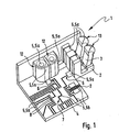
- FIG. 1 shows a conductor carrier according to the invention, designated by reference number 1, which has been manufactured using the production method according to the invention.
- the injection-molded conductor carrier 1 is designed as a three-dimensional MID part. It contains a substrate body 2 consisting of at least two different plastic materials and composed of a first carrier substrate 3 and a second carrier substrate 4 integrally formed thereon by injection molding.
- FIG. 2 shows the first carrier substrate 3 after its injection molding.
- This first carrier substrate 3 is expediently produced in time before the second carrier substrate 4.
- the second carrier substrate 4 is molded onto the first carrier substrate 3 in a desired manner by injection molding. Since both carrier substrates 3, 4 consist of plastic material, the substrate body 2 thus constitutes a 2-component injection-molded part.
- the substrate body 2 is coated on its surface with an electrical conductor arrangement 5. It consists of a metallization which has been deposited galvanically on predetermined regions of the substrate body 2.
- First components 5a of the electrical conductor arrangement 5 extend on the first carrier substrate 3.
- Second components 5b of the electrical conductor arrangement 5 run on the surface of the second carrier substrate 4. At one or more transition points 6 at least some of the first and second components 5a, 5b are in one another electrical connection, since there is an uninterrupted metallization here.
- the second components 5b of the electrical conductor arrangement 5 formed on the second carrier substrate 4 can represent a fine conductor structure as shown. It is composed of one or more relatively thin conductor tracks, wherein width dimensions of the individual conductor tracks of less than 100 microns can be realized.
- the conductor arrangement 5 can define on the second carrier substrate 4, as illustrated, a connection zone 7 at which a plurality of conductor tracks terminate with connection pads 8 defined by the metallization, on which a electronic component, such as a chip, can be contacted and fixed. In this way, an electronic circuit can be realized without problems.
- the first components 5a can have a very complex and also relatively high three-dimensional structuring.
- connection sockets 12 instead of the connection sockets 12, other connection components could also be provided.
- the electrical conductor arrangement could also be located on the first carrier substrate 3, for example on shielding regions or plated-through holes.
- the first carrier substrate 3 is first produced from a first plastic material 14 by injection molding.
- the shape of the first carrier substrate 3 is based on the desired structure of the conductor carrier 1, which in turn depends on the intended use.
- the conductor carrier 1 may be part of an electronic control or a sensor, but all other fields of application are open, for example as components of electronic circuits in communication technology or automation technology.
- the first carrier substrate 3 produced by injection molding has inter alia the uncoated connection sockets 12 and spring contacts 13.
- the first plastic material 14, from which the first carrier substrate 3 is produced is galvanically metallizable. It is therefore suitable to use the usual galvanic metallization techniques, as described for example in EP 0782765 B1, to be metallized over the entire surface.
- Plastics with the designation PA66-GF, PC / ABS or LCP are especially recommended as plastic material.
- the substrate body 2 shown in FIG. 3 is then present, which is composed of the two plastic components 14, 15 or the two carrier substrates 3, 4.
- the substrate body 2 is a rigid structural unit.
- the injection of the second plastic material 15 to the first carrier substrate 3 is done in such a way that predetermined areas of the first carrier substrate 3 are covered by the second plastic material 15 and in turn other areas remain uncovered.
- Various uncovered areas are identified by the reference numeral 16 in FIG.
- Such areas, which are covered by the molded-on second plastic material 15, are indicated by way of example in FIG. 2 at 17.
- the selective release and covering of certain areas of the first carrier substrate 3 is done by appropriate design of the mold, in which the second plastic material 15 to the first plastic material 14 and the first carrier substrate 3 is formed.
- the second plastic material 15 is formed so that it is basically not metallizable. It can therefore not be metallized with the usual steps, which are described for example in EP 0782765 B1.
- the second plastic material 15 advantageously still has the further property of laser beam activatable to be.
- the second carrier substrate 4 is subjected to a direct laser structuring in selected areas after the injection-molding of the substrate body 2 on the surface.
- a snapshot of this activation process is indicated in Figure 3 at 18.
- the second plastic material is, for example, a PBT plastic (polybutylene terephthalate) optimized for MID inserts, wherein the plastic material is provided with embedded laser-activatable metal particles or metal nuclei, for example of palladium or copper.
- PBT plastic polybutylene terephthalate
- the plastic material is provided with embedded laser-activatable metal particles or metal nuclei, for example of palladium or copper.
- plastic material of the designation PA6 / 6TMID, PBTMID or PPMID which is marketed by LPKF Laser & Electronics AG, 30827 Garbsen, Germany. Further materials are in preparation.
- a local activation of the substrate surface takes place, by means of which the desired circuit layout is produced.
- a local material activation takes place.
- metal nuclei are split off from special, non-conductive active substances or the metal nucleation is broken up.
- other fillers of the plastic material can produce a pronounced roughness on the irradiated surface areas.
- correspondingly activated metallization patterns 24 are produced on the second carrier substrate which can not be metallized from the start, on which metallization can now take place in a subsequent galvanic metallization process.
- the laser track following copper metallization takes place, wherein the roughness is a very good Liability for the resulting in the electroplating metal layer is ensured.
- the substrate body 2 which has a plurality of galvanically metallizable surface areas. These galvanically metallizable surface regions are, on the one hand, the uncovered regions 16 of the first carrier substrate 3 and, on the other hand, the metallization pattern 24 produced by laser direct structuring.
- the substrate body 2 is now subjected to a total galvanic treatment, wherein in the aforementioned zones, the metal contained in the electroplating bath, in particular copper, deposits. This results in the said zones a continuous metallization, which forms the electrical conductor arrangement 5 ( Figure 1).
- the metallization pattern 24 was previously formed such that it adjoins the corresponding surface regions 6 'directly to an uncovered region 16 of the first carrier substrate 3. As a result, an uninterrupted, continuous metallization at the transition points 6 is ensured.
Landscapes
- Engineering & Computer Science (AREA)
- Manufacturing & Machinery (AREA)
- Microelectronics & Electronic Packaging (AREA)
- Chemical & Material Sciences (AREA)
- Chemical Kinetics & Catalysis (AREA)
- Manufacturing Of Printed Wiring (AREA)
- Injection Moulding Of Plastics Or The Like (AREA)
- Structure Of Printed Boards (AREA)
- Conductive Materials (AREA)
Claims (7)
- Support de circuit imprimé moulé par injection, avec un premier substrat de support (3) composé d'une première matière plastique métallisable par galvanisation (14), sans activation au laser préalable, substrat sur lequel un deuxième substrat de support (4) est rapporté par moulage par injection de telle sorte que le premier substrat de support (3) reste en partie à découvert, caractérisé en ce que le deuxième substrat de support (4) se compose d'une deuxième matière plastique (15) métallisable par galvanisation uniquement dans des zones activées au laser, un ensemble de conducteurs électriques (5) s'étendant à travers les deux substrats de support (3, 4) qui se compose d'une métallisation se trouvant dans les zones à découvert (16) du premier substrat de support (3) et dans les zones activées au laser (24) du deuxième substrat de support (4).
- Support de circuit imprimé selon la revendication 1, caractérisé en ce que l'ensemble de conducteurs (5) s'étend sur le premier substrat de support (3) sur des éléments formant ressort (13) ou des composants de connexion (12) formés par des composants intégrés du premier substrat de support (3).
- Support de circuit imprimé selon la revendication 1 ou 2, caractérisé en ce que l'ensemble de conducteurs (5) est réalisé sur le deuxième substrat de support (4) comme une structure de conducteurs fins.
- Support de circuit imprimé selon l'une des revendications 1 à 3, caractérisé en ce que les zones activées au laser (24) du deuxième substrat de support (4) sont adjacentes à des zones à découvert (16') réalisées sur une grande surface, à la manière d'une plage de contact, du premier substrat de support (3).
- Support de circuit imprimé selon l'une des revendications 1 à 4, caractérisé en ce que la première matière plastique (14) est une matière de la spécification PA66-GF, PC/ABS ou LCP (Vectra E820i-Pd) et en ce que la deuxième matière plastique (15) est une matière de la spécification PA6/6TMID, PBTMID ou PPMID.
- Procédé de fabrication d'un support de circuit imprimé moulé par injection en utilisant un procédé de moulage par injection à deux composants, caractérisé en ce qu'une première matière plastique (14) métallisable par galvanisation, sans activation au laser préalable, et une deuxième matière plastique (15) métallisable par galvanisation uniquement dans des zones activées au laser sont rapportées l'une à l'autre par moulage par injection de telle sorte qu'un corps de substrat (2) est créé qui comprend un premier substrat de support (3) composé de la première matière plastique (14) et un deuxième substrat de support (4) composé de la deuxième matière plastique (15) et recouvrant partiellement le premier substrat de support (3), après quoi, sur le deuxième substrat de support (4), un motif de métallisation (24) est généré par activation au laser au moyen d'un faisceau laser (23) déplacé sur la surface du deuxième substrat de support (4), le motif étant adjacent au moins en partie à une ou plusieurs zones à découvert (16, 16') du premier substrat de support (3), et après quoi, une métallisation utilisable en tant qu'ensemble de conducteurs électriques (5) est déposée par galvanisation en même temps sur le motif de métallisation (24) et les zones à découvert (16, 16').
- Procédé selon la revendication 6, caractérisé en ce que l'on utilise comme première matière plastique une matière de la spécification PA66-GF, PC/ABS ou LCP (Vectra E820i Pd) et comme deuxième matière plastique (15) une matière de la spécification PA6/6TMID, PBTMID ou PPMID.
Priority Applications (5)
| Application Number | Priority Date | Filing Date | Title |
|---|---|---|---|
| AT02015961T ATE350884T1 (de) | 2002-07-18 | 2002-07-18 | Spritzgegossener leiterträger und verfahren zu seiner herstellung |
| EP02015961A EP1383360B1 (fr) | 2002-07-18 | 2002-07-18 | Support de circuit imprimé moulé par injection et son procédé de fabrication |
| DE50209164T DE50209164D1 (de) | 2002-07-18 | 2002-07-18 | Spritzgegossener Leiterträger und Verfahren zu seiner Herstellung |
| US10/617,925 US7276267B2 (en) | 2002-07-18 | 2003-07-11 | Method for the manufacture of an injection molded conductor carrying means |
| JP2003276930A JP4152274B2 (ja) | 2002-07-18 | 2003-07-18 | 射出成形コンダクタ支持装置及びその製造方法 |
Applications Claiming Priority (1)
| Application Number | Priority Date | Filing Date | Title |
|---|---|---|---|
| EP02015961A EP1383360B1 (fr) | 2002-07-18 | 2002-07-18 | Support de circuit imprimé moulé par injection et son procédé de fabrication |
Publications (2)
| Publication Number | Publication Date |
|---|---|
| EP1383360A1 EP1383360A1 (fr) | 2004-01-21 |
| EP1383360B1 true EP1383360B1 (fr) | 2007-01-03 |
Family
ID=29762648
Family Applications (1)
| Application Number | Title | Priority Date | Filing Date |
|---|---|---|---|
| EP02015961A Expired - Lifetime EP1383360B1 (fr) | 2002-07-18 | 2002-07-18 | Support de circuit imprimé moulé par injection et son procédé de fabrication |
Country Status (5)
| Country | Link |
|---|---|
| US (1) | US7276267B2 (fr) |
| EP (1) | EP1383360B1 (fr) |
| JP (1) | JP4152274B2 (fr) |
| AT (1) | ATE350884T1 (fr) |
| DE (1) | DE50209164D1 (fr) |
Families Citing this family (30)
| Publication number | Priority date | Publication date | Assignee | Title |
|---|---|---|---|---|
| DE20309009U1 (de) | 2003-06-11 | 2003-08-14 | FESTO AG & Co., 73734 Esslingen | Elektrisches Bauteil, insbesondere Positionssensor |
| DE102004035284B4 (de) * | 2004-07-21 | 2008-10-02 | Festo Ag & Co. Kg | Positionssensoranordnung mit mehreren in einer Reihe angeordneten, magnetfeldsensitiven Sensoren, insbesondere Hall-Sensoren |
| DE502005005709D1 (de) * | 2005-10-25 | 2008-11-27 | Roche Diagnostics Gmbh | Analysegerät zur Analyse einer Probe auf einem Testelement |
| US8816184B2 (en) * | 2005-12-01 | 2014-08-26 | Raytheon Company | Thermoelectric bias voltage generator |
| US7358921B2 (en) * | 2005-12-01 | 2008-04-15 | Harris Corporation | Dual polarization antenna and associated methods |
| DE102006041610B3 (de) * | 2006-09-05 | 2008-05-08 | Harting Mitronics Ag | Metallisierte Kunststoffoberfläche und Verfahren zum Bearbeiten von metallisierten Kunststoffoberflächen |
| EP1930216A1 (fr) * | 2006-12-07 | 2008-06-11 | Nederlandse Organisatie voor toegepast-natuurwetenschappelijk Onderzoek TNO | Faisceau de câbles |
| US8059415B2 (en) * | 2006-12-15 | 2011-11-15 | Finisar Corporation | Molded communications module having integrated plastic circuit structures |
| US7789674B2 (en) * | 2007-05-02 | 2010-09-07 | Finisar Corporation | Molded card edge connector for attachment with a printed circuit board |
| US7804450B2 (en) * | 2007-07-20 | 2010-09-28 | Laird Technologies, Inc. | Hybrid antenna structure |
| DE102007044359A1 (de) | 2007-09-17 | 2009-03-19 | Robert Bosch Gmbh | LDS Stecker |
| US8400319B2 (en) * | 2007-09-24 | 2013-03-19 | John Mezzalingua Associates, Inc. | Coaxial cable connector with an external sensor and method of use thereof |
| US8149127B2 (en) * | 2007-09-24 | 2012-04-03 | John Mezzalingua Associates, Inc. | Coaxial cable connector with an internal coupler and method of use thereof |
| US8773255B2 (en) * | 2007-09-24 | 2014-07-08 | Ppc Broadband, Inc. | Status sensing and reporting interface |
| US8570178B2 (en) * | 2007-09-24 | 2013-10-29 | Ppc Broadband, Inc. | Coaxial cable connector with internal floating ground circuitry and method of use thereof |
| US8400318B2 (en) * | 2007-09-24 | 2013-03-19 | John Mezzalingua Associates, Inc. | Method for determining electrical power signal levels in a transmission system |
| US8414326B2 (en) * | 2008-11-17 | 2013-04-09 | Rochester Institute Of Technology | Internal coaxial cable connector integrated circuit and method of use thereof |
| US8376774B2 (en) * | 2008-11-17 | 2013-02-19 | Rochester Institute Of Technology | Power extracting device and method of use thereof |
| US8303334B2 (en) * | 2008-11-17 | 2012-11-06 | John Mezzalingua Associates, Inc. | Embedded coupler device and method of use thereof |
| US8419464B2 (en) * | 2008-11-17 | 2013-04-16 | Ppc Broadband, Inc. | Coaxial connector with integrated molded substrate and method of use thereof |
| US20110073480A1 (en) * | 2009-09-29 | 2011-03-31 | Chih-Yeh Chou | Process of Manufacturing Low-Profile Connector |
| US8618944B2 (en) * | 2009-12-03 | 2013-12-31 | Ppc Broadband, Inc. | Coaxial cable connector parameter monitoring system |
| US8974869B2 (en) * | 2010-01-26 | 2015-03-10 | Robert Hamilton | Method for improving plating on non-conductive substrates |
| US20120273261A1 (en) | 2010-10-20 | 2012-11-01 | Taiwan Green Point Enterprises Co., Ltd. | Circuit substrate having a circuit pattern and method for making the same |
| US8621749B2 (en) | 2010-03-12 | 2014-01-07 | Taiwan Green Point Enterprises Co., Ltd | Non-deleterious technique for creating continuous conductive circuits |
| US8952919B2 (en) | 2011-02-25 | 2015-02-10 | Taiwan Green Point Enterprises Co., Ltd. | Capacitive touch sensitive housing and method for making the same |
| US8604936B2 (en) | 2010-12-13 | 2013-12-10 | Ppc Broadband, Inc. | Coaxial cable connector, system and method of use thereof |
| US8827557B2 (en) * | 2011-03-09 | 2014-09-09 | Curwood, Inc. | Gusseted bag with easy-open lap seal |
| JP6230625B2 (ja) * | 2014-01-14 | 2017-11-15 | 太陽インキ製造株式会社 | 立体回路基板およびこれに用いるソルダーレジスト組成物 |
| CN113498271A (zh) * | 2021-06-04 | 2021-10-12 | 深圳市信维通信股份有限公司 | 一种pcb板注塑体的制备工艺 |
Family Cites Families (8)
| Publication number | Priority date | Publication date | Assignee | Title |
|---|---|---|---|---|
| IN167760B (fr) * | 1986-08-15 | 1990-12-15 | Kollmorgen Tech Corp | |
| JPH0660416B2 (ja) * | 1986-11-18 | 1994-08-10 | 三共化成株式会社 | プラスチック成形品の製法 |
| US4812353A (en) * | 1986-12-27 | 1989-03-14 | Sankyo Kasei Kabushiki Kaisha | Process for the production of circuit board and the like |
| JPH0773155B2 (ja) * | 1992-04-20 | 1995-08-02 | 大宏電機株式会社 | 回路部品の製造方法 |
| JP2923145B2 (ja) * | 1992-10-28 | 1999-07-26 | 日立電線株式会社 | 回路端子付プラスチック成形品 |
| KR100279196B1 (ko) | 1994-09-23 | 2001-02-01 | 에르. 반 오버슈트래텐 | 폴리머 스터드 그리드 어레이 |
| DE19921660A1 (de) * | 1999-05-11 | 2000-11-30 | Festo Ag & Co | Mikroventilanordnung |
| TW526689B (en) * | 2000-06-12 | 2003-04-01 | Bourns Inc | Molded electronic assembly |
-
2002
- 2002-07-18 AT AT02015961T patent/ATE350884T1/de active
- 2002-07-18 DE DE50209164T patent/DE50209164D1/de not_active Expired - Lifetime
- 2002-07-18 EP EP02015961A patent/EP1383360B1/fr not_active Expired - Lifetime
-
2003
- 2003-07-11 US US10/617,925 patent/US7276267B2/en not_active Expired - Fee Related
- 2003-07-18 JP JP2003276930A patent/JP4152274B2/ja not_active Expired - Fee Related
Also Published As
| Publication number | Publication date |
|---|---|
| JP4152274B2 (ja) | 2008-09-17 |
| DE50209164D1 (de) | 2007-02-15 |
| JP2004056149A (ja) | 2004-02-19 |
| EP1383360A1 (fr) | 2004-01-21 |
| ATE350884T1 (de) | 2007-01-15 |
| US20040104040A1 (en) | 2004-06-03 |
| US7276267B2 (en) | 2007-10-02 |
Similar Documents
| Publication | Publication Date | Title |
|---|---|---|
| EP1383360B1 (fr) | Support de circuit imprimé moulé par injection et son procédé de fabrication | |
| DE112015006047B4 (de) | Herstellungsverfahren für eine räumliche leiterplatte, räumliche leiterplatte und substrat für eine räumliche leiterplatte | |
| DE102007009583A1 (de) | Verbundformteil | |
| EP0485838B1 (fr) | Plaques à circuit moulées par injection arrière de circuits flexibles par des matériaux thermoplastiques | |
| DE3605342A1 (de) | Fuer das aufbringen festhaftender metallbelaege geeignete formkoerper, metallisierte formkoerper sowie verfahren zu deren herstellung | |
| EP0929428B1 (fr) | Appareil de regulation de vanne avec carte de circuits tridimensionnelle realisee selon la technique des dispositifs d'interconnexion moules | |
| EP1432278B1 (fr) | Module de microphone pour une prothèse auditive | |
| EP2499314B1 (fr) | Procédé de fabrication d'une serrure de porte de véhicule automobile et serrure de porte de véhicule automobile associée | |
| DE19755398A1 (de) | Verfahren zur Herstellung eines mehrschichtigen dreidimensionalen Schaltkreises | |
| DE4416986A1 (de) | Verfahren zum Herstellen eines Bauteils aus thermoplastischem Kunststoff mit wenigstens einem integrierten, elektrisch leitenden Abschnitt sowie nach diesem Verfahren hergestelltes Bauteil | |
| EP2819492A1 (fr) | Composant MID, procédé de fabrication | |
| EP1351551B1 (fr) | Dispositif de contact pour prothèse auditive | |
| EP0645953A1 (fr) | Procédé de fabrication d'un câblage à deux ou plusieurs couches, et câblage à deux ou plusieurs couches | |
| DE4432966A1 (de) | Verfahren zum Herstellen eines Bauteils aus thermoplastischem Kunststoff mit wenigstens einem integrierten, elektrisch leitenden Abschnitt sowie nach diesem Verfahren hergestelltes Bauteil | |
| DE19517338A1 (de) | Verfahren zum selektiven Beschichten eines Kunststofferzeugnisses und nach diesem Verfahren hergestelltes Erzeugnis | |
| DE102016213326A1 (de) | Gehäuseanordnung für eine kraftbetriebene Vorrichtung und Verfahren zu seiner Herstellung | |
| DE10234125A1 (de) | Beleuchtbares Kunststoffspritzgussteil mit einer Anzeigefunktion und Verfahren zu dessen Herstellung | |
| EP1079672A2 (fr) | Article en plastique comportant des contacts électriques | |
| DE102019006445B4 (de) | Verfahren zur Herstellung eines Bauteils | |
| DE2920091A1 (de) | Kunststoff-formteil | |
| EP0784418A2 (fr) | Procédé de fabrication de corps moulés à circuit, dits 3-D MID | |
| EP1501341B1 (fr) | Aménagement de positionnement de pistes conductrices | |
| EP0543045B1 (fr) | Procédé de fabrication de plaques à circuit imprimé | |
| DE102008003372B4 (de) | Verfahren zur Herstellung eines mehrlagigen zwei- oder dreidimensionalen Schaltungsträgers | |
| DE19726850B4 (de) | Verfahren zur Herstellung vonr Leiterplatten |
Legal Events
| Date | Code | Title | Description |
|---|---|---|---|
| PUAI | Public reference made under article 153(3) epc to a published international application that has entered the european phase |
Free format text: ORIGINAL CODE: 0009012 |
|
| AK | Designated contracting states |
Kind code of ref document: A1 Designated state(s): AT BE BG CH CY CZ DE DK EE ES FI FR GB GR IE IT LI LU MC NL PT SE SK TR |
|
| AX | Request for extension of the european patent |
Extension state: AL LT LV MK RO SI |
|
| 17P | Request for examination filed |
Effective date: 20040119 |
|
| AKX | Designation fees paid |
Designated state(s): AT BE BG CH CY CZ DE DK EE ES FI FR GB GR IE IT LI LU MC NL PT SE SK TR |
|
| GRAP | Despatch of communication of intention to grant a patent |
Free format text: ORIGINAL CODE: EPIDOSNIGR1 |
|
| RIC1 | Information provided on ipc code assigned before grant |
Ipc: H05K 3/00 20060101ALI20060628BHEP Ipc: H05K 1/00 20060101AFI20060628BHEP Ipc: H05K 3/18 20060101ALI20060628BHEP |
|
| GRAS | Grant fee paid |
Free format text: ORIGINAL CODE: EPIDOSNIGR3 |
|
| GRAA | (expected) grant |
Free format text: ORIGINAL CODE: 0009210 |
|
| AK | Designated contracting states |
Kind code of ref document: B1 Designated state(s): AT BE BG CH CY CZ DE DK EE ES FI FR GB GR IE IT LI LU MC NL PT SE SK TR |
|
| PG25 | Lapsed in a contracting state [announced via postgrant information from national office to epo] |
Ref country code: DK Free format text: LAPSE BECAUSE OF FAILURE TO SUBMIT A TRANSLATION OF THE DESCRIPTION OR TO PAY THE FEE WITHIN THE PRESCRIBED TIME-LIMIT Effective date: 20070103 |
|
| REG | Reference to a national code |
Ref country code: GB Ref legal event code: FG4D Free format text: NOT ENGLISH |
|
| REF | Corresponds to: |
Ref document number: 50209164 Country of ref document: DE Date of ref document: 20070215 Kind code of ref document: P |
|
| REG | Reference to a national code |
Ref country code: IE Ref legal event code: FG4D Free format text: LANGUAGE OF EP DOCUMENT: GERMAN |
|
| GBT | Gb: translation of ep patent filed (gb section 77(6)(a)/1977) |
Effective date: 20070205 |
|
| PG25 | Lapsed in a contracting state [announced via postgrant information from national office to epo] |
Ref country code: SE Free format text: LAPSE BECAUSE OF FAILURE TO SUBMIT A TRANSLATION OF THE DESCRIPTION OR TO PAY THE FEE WITHIN THE PRESCRIBED TIME-LIMIT Effective date: 20070403 |
|
| PG25 | Lapsed in a contracting state [announced via postgrant information from national office to epo] |
Ref country code: ES Free format text: LAPSE BECAUSE OF FAILURE TO SUBMIT A TRANSLATION OF THE DESCRIPTION OR TO PAY THE FEE WITHIN THE PRESCRIBED TIME-LIMIT Effective date: 20070414 |
|
| ET | Fr: translation filed | ||
| PLBE | No opposition filed within time limit |
Free format text: ORIGINAL CODE: 0009261 |
|
| STAA | Information on the status of an ep patent application or granted ep patent |
Free format text: STATUS: NO OPPOSITION FILED WITHIN TIME LIMIT |
|
| PG25 | Lapsed in a contracting state [announced via postgrant information from national office to epo] |
Ref country code: SK Free format text: LAPSE BECAUSE OF FAILURE TO SUBMIT A TRANSLATION OF THE DESCRIPTION OR TO PAY THE FEE WITHIN THE PRESCRIBED TIME-LIMIT Effective date: 20070103 |
|
| 26N | No opposition filed |
Effective date: 20071005 |
|
| PG25 | Lapsed in a contracting state [announced via postgrant information from national office to epo] |
Ref country code: CZ Free format text: LAPSE BECAUSE OF FAILURE TO SUBMIT A TRANSLATION OF THE DESCRIPTION OR TO PAY THE FEE WITHIN THE PRESCRIBED TIME-LIMIT Effective date: 20070103 |
|
| BERE | Be: lapsed |
Owner name: FESTO A.G. & CO. Effective date: 20070731 |
|
| PG25 | Lapsed in a contracting state [announced via postgrant information from national office to epo] |
Ref country code: GR Free format text: LAPSE BECAUSE OF FAILURE TO SUBMIT A TRANSLATION OF THE DESCRIPTION OR TO PAY THE FEE WITHIN THE PRESCRIBED TIME-LIMIT Effective date: 20070404 Ref country code: MC Free format text: LAPSE BECAUSE OF NON-PAYMENT OF DUE FEES Effective date: 20070731 |
|
| PG25 | Lapsed in a contracting state [announced via postgrant information from national office to epo] |
Ref country code: BE Free format text: LAPSE BECAUSE OF NON-PAYMENT OF DUE FEES Effective date: 20070731 |
|
| PGFP | Annual fee paid to national office [announced via postgrant information from national office to epo] |
Ref country code: IE Payment date: 20080707 Year of fee payment: 7 |
|
| PG25 | Lapsed in a contracting state [announced via postgrant information from national office to epo] |
Ref country code: EE Free format text: LAPSE BECAUSE OF FAILURE TO SUBMIT A TRANSLATION OF THE DESCRIPTION OR TO PAY THE FEE WITHIN THE PRESCRIBED TIME-LIMIT Effective date: 20070103 |
|
| PG25 | Lapsed in a contracting state [announced via postgrant information from national office to epo] |
Ref country code: CY Free format text: LAPSE BECAUSE OF FAILURE TO SUBMIT A TRANSLATION OF THE DESCRIPTION OR TO PAY THE FEE WITHIN THE PRESCRIBED TIME-LIMIT Effective date: 20070103 |
|
| PG25 | Lapsed in a contracting state [announced via postgrant information from national office to epo] |
Ref country code: LU Free format text: LAPSE BECAUSE OF NON-PAYMENT OF DUE FEES Effective date: 20070718 |
|
| PG25 | Lapsed in a contracting state [announced via postgrant information from national office to epo] |
Ref country code: TR Free format text: LAPSE BECAUSE OF FAILURE TO SUBMIT A TRANSLATION OF THE DESCRIPTION OR TO PAY THE FEE WITHIN THE PRESCRIBED TIME-LIMIT Effective date: 20070103 |
|
| PG25 | Lapsed in a contracting state [announced via postgrant information from national office to epo] |
Ref country code: IE Free format text: LAPSE BECAUSE OF NON-PAYMENT OF DUE FEES Effective date: 20090720 |
|
| PGFP | Annual fee paid to national office [announced via postgrant information from national office to epo] |
Ref country code: BG Payment date: 20110531 Year of fee payment: 10 |
|
| PGFP | Annual fee paid to national office [announced via postgrant information from national office to epo] |
Ref country code: FI Payment date: 20120704 Year of fee payment: 11 |
|
| PGFP | Annual fee paid to national office [announced via postgrant information from national office to epo] |
Ref country code: NL Payment date: 20120716 Year of fee payment: 11 |
|
| PGFP | Annual fee paid to national office [announced via postgrant information from national office to epo] |
Ref country code: FR Payment date: 20130719 Year of fee payment: 12 |
|
| REG | Reference to a national code |
Ref country code: NL Ref legal event code: V1 Effective date: 20140201 |
|
| PG25 | Lapsed in a contracting state [announced via postgrant information from national office to epo] |
Ref country code: NL Free format text: LAPSE BECAUSE OF NON-PAYMENT OF DUE FEES Effective date: 20140201 Ref country code: FI Free format text: LAPSE BECAUSE OF NON-PAYMENT OF DUE FEES Effective date: 20130718 |
|
| PGFP | Annual fee paid to national office [announced via postgrant information from national office to epo] |
Ref country code: GB Payment date: 20140530 Year of fee payment: 13 |
|
| PG25 | Lapsed in a contracting state [announced via postgrant information from national office to epo] |
Ref country code: BG Free format text: LAPSE BECAUSE OF NON-PAYMENT OF DUE FEES Effective date: 20120731 Ref country code: PT Free format text: LAPSE BECAUSE OF NON-PAYMENT OF DUE FEES Effective date: 20070604 |
|
| PGFP | Annual fee paid to national office [announced via postgrant information from national office to epo] |
Ref country code: AT Payment date: 20140716 Year of fee payment: 13 |
|
| PGFP | Annual fee paid to national office [announced via postgrant information from national office to epo] |
Ref country code: IT Payment date: 20140704 Year of fee payment: 13 |
|
| REG | Reference to a national code |
Ref country code: FR Ref legal event code: ST Effective date: 20150331 |
|
| PG25 | Lapsed in a contracting state [announced via postgrant information from national office to epo] |
Ref country code: FR Free format text: LAPSE BECAUSE OF NON-PAYMENT OF DUE FEES Effective date: 20140731 |
|
| PGFP | Annual fee paid to national office [announced via postgrant information from national office to epo] |
Ref country code: CH Payment date: 20150723 Year of fee payment: 14 Ref country code: DE Payment date: 20150530 Year of fee payment: 14 |
|
| REG | Reference to a national code |
Ref country code: AT Ref legal event code: MM01 Ref document number: 350884 Country of ref document: AT Kind code of ref document: T Effective date: 20150718 |
|
| GBPC | Gb: european patent ceased through non-payment of renewal fee |
Effective date: 20150718 |
|
| PG25 | Lapsed in a contracting state [announced via postgrant information from national office to epo] |
Ref country code: GB Free format text: LAPSE BECAUSE OF NON-PAYMENT OF DUE FEES Effective date: 20150718 Ref country code: IT Free format text: LAPSE BECAUSE OF NON-PAYMENT OF DUE FEES Effective date: 20150718 |
|
| PG25 | Lapsed in a contracting state [announced via postgrant information from national office to epo] |
Ref country code: AT Free format text: LAPSE BECAUSE OF NON-PAYMENT OF DUE FEES Effective date: 20150718 |
|
| REG | Reference to a national code |
Ref country code: DE Ref legal event code: R119 Ref document number: 50209164 Country of ref document: DE |
|
| REG | Reference to a national code |
Ref country code: CH Ref legal event code: PL |
|
| PG25 | Lapsed in a contracting state [announced via postgrant information from national office to epo] |
Ref country code: DE Free format text: LAPSE BECAUSE OF NON-PAYMENT OF DUE FEES Effective date: 20170201 Ref country code: CH Free format text: LAPSE BECAUSE OF NON-PAYMENT OF DUE FEES Effective date: 20160731 Ref country code: LI Free format text: LAPSE BECAUSE OF NON-PAYMENT OF DUE FEES Effective date: 20160731 |