EP1387247A2 - Système et procédé d' empilage et desempilage automatique de variables locales Java - Google Patents
Système et procédé d' empilage et desempilage automatique de variables locales Java Download PDFInfo
- Publication number
- EP1387247A2 EP1387247A2 EP03291905A EP03291905A EP1387247A2 EP 1387247 A2 EP1387247 A2 EP 1387247A2 EP 03291905 A EP03291905 A EP 03291905A EP 03291905 A EP03291905 A EP 03291905A EP 1387247 A2 EP1387247 A2 EP 1387247A2
- Authority
- EP
- European Patent Office
- Prior art keywords
- pointer
- cache
- local variables
- local
- data
- Prior art date
- Legal status (The legal status is an assumption and is not a legal conclusion. Google has not performed a legal analysis and makes no representation as to the accuracy of the status listed.)
- Withdrawn
Links
Images


Classifications
-
- G—PHYSICS
- G06—COMPUTING OR CALCULATING; COUNTING
- G06F—ELECTRIC DIGITAL DATA PROCESSING
- G06F12/00—Accessing, addressing or allocating within memory systems or architectures
- G06F12/02—Addressing or allocation; Relocation
- G06F12/08—Addressing or allocation; Relocation in hierarchically structured memory systems, e.g. virtual memory systems
- G06F12/12—Replacement control
- G06F12/121—Replacement control using replacement algorithms
- G06F12/126—Replacement control using replacement algorithms with special data handling, e.g. priority of data or instructions, handling errors or pinning
-
- G—PHYSICS
- G06—COMPUTING OR CALCULATING; COUNTING
- G06F—ELECTRIC DIGITAL DATA PROCESSING
- G06F12/00—Accessing, addressing or allocating within memory systems or architectures
- G06F12/02—Addressing or allocation; Relocation
- G06F12/0223—User address space allocation, e.g. contiguous or non contiguous base addressing
- G06F12/023—Free address space management
- G06F12/0253—Garbage collection, i.e. reclamation of unreferenced memory
-
- G—PHYSICS
- G06—COMPUTING OR CALCULATING; COUNTING
- G06F—ELECTRIC DIGITAL DATA PROCESSING
- G06F12/00—Accessing, addressing or allocating within memory systems or architectures
- G06F12/02—Addressing or allocation; Relocation
- G06F12/08—Addressing or allocation; Relocation in hierarchically structured memory systems, e.g. virtual memory systems
- G06F12/0802—Addressing of a memory level in which the access to the desired data or data block requires associative addressing means, e.g. caches
- G06F12/0804—Addressing of a memory level in which the access to the desired data or data block requires associative addressing means, e.g. caches with main memory updating
-
- G—PHYSICS
- G06—COMPUTING OR CALCULATING; COUNTING
- G06F—ELECTRIC DIGITAL DATA PROCESSING
- G06F12/00—Accessing, addressing or allocating within memory systems or architectures
- G06F12/02—Addressing or allocation; Relocation
- G06F12/08—Addressing or allocation; Relocation in hierarchically structured memory systems, e.g. virtual memory systems
- G06F12/0802—Addressing of a memory level in which the access to the desired data or data block requires associative addressing means, e.g. caches
- G06F12/0891—Addressing of a memory level in which the access to the desired data or data block requires associative addressing means, e.g. caches using clearing, invalidating or resetting means
-
- G—PHYSICS
- G06—COMPUTING OR CALCULATING; COUNTING
- G06F—ELECTRIC DIGITAL DATA PROCESSING
- G06F9/00—Arrangements for program control, e.g. control units
- G06F9/06—Arrangements for program control, e.g. control units using stored programs, i.e. using an internal store of processing equipment to receive or retain programs
- G06F9/30—Arrangements for executing machine instructions, e.g. instruction decode
- G06F9/30181—Instruction operation extension or modification
- G06F9/30189—Instruction operation extension or modification according to execution mode, e.g. mode flag
-
- G—PHYSICS
- G06—COMPUTING OR CALCULATING; COUNTING
- G06F—ELECTRIC DIGITAL DATA PROCESSING
- G06F9/00—Arrangements for program control, e.g. control units
- G06F9/06—Arrangements for program control, e.g. control units using stored programs, i.e. using an internal store of processing equipment to receive or retain programs
- G06F9/44—Arrangements for executing specific programs
- G06F9/448—Execution paradigms, e.g. implementations of programming paradigms
- G06F9/4482—Procedural
- G06F9/4484—Executing subprograms
-
- G—PHYSICS
- G06—COMPUTING OR CALCULATING; COUNTING
- G06F—ELECTRIC DIGITAL DATA PROCESSING
- G06F2212/00—Indexing scheme relating to accessing, addressing or allocation within memory systems or architectures
- G06F2212/50—Control mechanisms for virtual memory, cache or TLB
- G06F2212/502—Control mechanisms for virtual memory, cache or TLB using adaptive policy
-
- Y—GENERAL TAGGING OF NEW TECHNOLOGICAL DEVELOPMENTS; GENERAL TAGGING OF CROSS-SECTIONAL TECHNOLOGIES SPANNING OVER SEVERAL SECTIONS OF THE IPC; TECHNICAL SUBJECTS COVERED BY FORMER USPC CROSS-REFERENCE ART COLLECTIONS [XRACs] AND DIGESTS
- Y02—TECHNOLOGIES OR APPLICATIONS FOR MITIGATION OR ADAPTATION AGAINST CLIMATE CHANGE
- Y02D—CLIMATE CHANGE MITIGATION TECHNOLOGIES IN INFORMATION AND COMMUNICATION TECHNOLOGIES [ICT], I.E. INFORMATION AND COMMUNICATION TECHNOLOGIES AIMING AT THE REDUCTION OF THEIR OWN ENERGY USE
- Y02D10/00—Energy efficient computing, e.g. low power processors, power management or thermal management
Definitions
- the present invention relates generally to processors and more particularly to managing local variables used by a processor.
- multimedia functionality may include, without limitation, games, audio decoders, digital cameras, etc. It is thus desirable to implement such functionality in an electronic device in a way that, all else being equal, is fast, consumes as little power as possible and requires as little memory as possible. Improvements in this area are desirable.
- a processor preferably comprises a processing core that generates memory addresses to access a memory and on which a plurality of methods operate, a cache coupled to the processing core, and a programmable register containing a pointer to a currently active method's set of local variables.
- the cache may be used to store one or more sets of local variables, each set being used by a method. Further, the cache may include at least two sets of local variables corresponding to different methods, one method calling the other method and the sets of local variables may be separated by a pointer to the set of local variables corresponding to the calling method.
- the subject matter disclosed herein is directed to a programmable electronic device such as a processor having memory in which "local variables" associated with a stack-based language (e.g., Java) and pointers associated with the local variables may be stored.
- the term "local variables” refers to temporary variables used by a method that executes on the processor. Multiple methods may run on the processor and each method preferably has its own set of local variables. In general, local variables have meaning only while their associated method is running.
- the stack-based language may comprise Java Bytecodes although this disclosure is not so limited. In Java Bytecodes, the notion of local variables (“LVs”) is equivalent to automatic variables in other programming languages (e.g., "C”) and other named variables in still other programming languages.
- Java is particularly suited for embedded applications.
- Java is a relatively "dense" language meaning that on average each instruction may perform a large number of functions compared to various other programming languages.
- the dense nature of Java is of particular benefit for portable, battery-operated devices that preferably include as little memory as possible to save space and power. The reason, however, for executing Java code is not material to this disclosure or the claims that follow.
- System 100 includes at least two processors 102 and 104.
- Processor 102 is referred to for purposes of this disclosure as a Java Stack Machine ("JSM") and processor 104 may be referred to as a Main Processor Unit (“MPU”) .
- System 100 may also include memory 106 coupled to both the JSM 102 and MPU 104 and thus accessible by both processors. At least a portion of the memory 106 may be shared by both processors meaning that both processors may access the same shared memory locations. Further, if desired, a portion of the memory 106 may be designated as private to one processor or the other.
- JSM Java Stack Machine
- MPU Main Processor Unit
- System 100 also includes a Java Virtual Machine (“JVM”) 108, compiler 110, and a display 114.
- the JSM 102 preferably includes an interface to one or more input/output (“I/O") devices such as a keypad to permit a user to control various aspects of the system 100.
- I/O input/output
- data streams may be received from the I/O space into the JSM 102 to be processed by the JSM 102.
- Other components may include, without limitation, a battery and an analog transceiver to permit wireless communications with other devices.
- system 100 may be representative of, or adapted to, a wide variety of electronic systems, an exemplary electronic system may comprise a battery-operated, mobile cell phone such as that shown in Figure 2.
- a mobile communications device includes an integrated keypad 412 and display 414.
- the JSM 102 and MPU 104 noted above and other components may be included in electronics package 410 which may be coupled to keypad 410, display 414, and radio frequency (“RF") circuitry 416 which may be connected to an antenna 418.
- RF radio frequency
- Java code comprises a plurality of "Bytecodes" 112.
- Bytecodes 112 may be provided to the JVM 108, compiled by compiler 110 and provided to the JSM 102 and/or MPU 104 for execution therein.
- the JSM 102 may execute at least some, and generally most, of the Java Bytecodes.
- the JSM 102 may request the MPU 104 to execute one or more Java Bytecodes not executed or executable by the JSM 102.
- the MPU 104 also may execute non-Java instructions.
- the MPU 104 also hosts an operating system ("O/S") (not specifically shown), which performs various functions including system memory management, the system task management that schedules the JVM 108 and most or all other native tasks running on the system, management of the display 114, receiving input from input devices, etc.
- O/S operating system
- Java code may be used to perform any one of a variety of applications including multimedia, games or web based applications in the system 100, while non-Java code, which may comprise the O/S and other native applications, may still run on the system on the MPU 104.
- the JVM 108 generally comprises a combination of software and hardware.
- the software may include the compiler 110 and the hardware may include the JSM 102.
- the JVM may include a class loader, bytecode verifier, garbage collector, and a bytecode interpreter loop to interpret the bytecodes that are not executed on the JSM processor 102.
- the JSM 102 may execute at least two instruction sets.
- One instruction set may comprise standard Java bytecodes.
- Java is a stack-based programming language in which instructions generally target a stack. For example, an integer add (“IADD") Java instruction pops two integers off the top of the stack, adds them together, and pushes the sum back on the stack.
- IADD integer add
- the JSM 102 comprises a stack-based architecture with various features that accelerate the execution of stack-based Java code.
- Another instruction set executed by the JSM 102 may include instructions other than standard Java instructions.
- such other instruction set may include register-based and memory-based operations to be performed.
- This other instruction set generally complements the Java instruction set and, accordingly, may be referred to as a complementary instruction set architecture ("C-ISA").
- C-ISA complementary instruction set architecture
- By complementary it is meant that the execution of more complex Java Bytecodes may be substituted by micro-seqeunces using C-ISA instructions that permits address calculation to readily "walk through" the JVM data structures. Further, such micro-sequences may also use Bytecode instructions.
- the execution of Java may be made more efficient and run faster by replacing some sequences of Bytecodes by preferably shorter and more efficient sequences of C-ISA instructions.
- Bytecodes may also be used within a C-ISA sequence.
- the two sets of instructions may be used in a complementary fashion to obtain satisfactory code density and efficiency.
- the JSM 102 generally comprises a stack-based architecture for efficient and accelerated execution of Java bytecodes combined with a register-based architecture for executing register and memory based C-ISA instructions. Both architectures preferably are tightly combined and integrated through the C-ISA.
- FIG. 3 shows an exemplary block diagram of the JSM 102.
- the JSM includes a core 120 coupled to data storage 122 and instruction storage 130.
- the core may include one or more components as shown.
- Such components preferably include a plurality of registers 140, three address generation units (“AGUs") 142, 147, micro-translation lookaside buffers (micro-TLBs) 144, 156, a multi-entry micro-stack 146, an arithmetic logic unit (“ALU”) 148, a multiplier 150, decode logic 152, and instruction fetch logic 154.
- AGUs address generation units
- micro-TLBs micro-translation lookaside buffers
- ALU arithmetic logic unit
- operands may be retrieved from data storage 122 or from the micro-stack 146, processed by the ALU 148, while instructions may be fetched from instruction storage 130 by fetch logic 154 and decoded by decode logic 152.
- the address generation unit 142 may be used to calculate addresses based, at least in part on data contained in the registers 140.
- the AGUs 142 may calculate addresses for C-ISA instructions as will be described below.
- the AGUs 142 may support parallel data accesses for C-ISA instructions that perform array or other types of processing.
- AGU 147 couples to the micro-stack 146 and may manage overflow and underflow conditions in the micro-stack preferably in parallel.
- the micro-TLBs 144, 156 generally perform the function of a cache for the address translation and memory protection information bits that are preferably under the control of the operating system running on the MPU 104.
- the registers 140 may include 16 registers designated as R0-R15.
- Registers R0-R3, R5, R8-R11 and R13-R14 may be used as general purposes ("GP") registers usable for any purpose by the programmer.
- Other registers, and some of the GP registers, may be used for specific functions.
- registers R4 and R12 may be used to store two program counters.
- Register R4 preferably is used to store the program counter (“PC") and register R12 preferably is used to store a micro-program counter ("micro-PC").
- register R5 may be used to store the base address of a portion of memory in which Java local variables may be stored when used by the currently executing Java method.
- the top of the micro-stack 146 may be referenced by the values in registers R6 and R7.
- the top of the micro-stack has a matching address in external memory pointed to by register R6.
- the values contained in the micro-stack are the latest updated values, while their corresponding values in external memory may or may not be up to date.
- Register R7 provides the data value stored at the top of the micro-stack.
- Registers R8 and R9 may also be used to hold the address index 0 ("AI0" and address index 1 ("AI1"), as will be explained below.
- Register R14 may also be used to hold the indirect register index ("IRI").
- Register R15 may be used for status and control of the JSM 102.
- the JSM 102 is adapted to process and execute instructions from at least two instruction sets and one or more methods comprising such instructions.
- One instruction set includes stack-based operations and the second instruction set includes register-based and memory-based operations.
- the stack-based instruction set may include Java Bytecodes. Java Bytecodes pop, unless empty, data from and push data onto the micro-stack 146.
- the micro-stack 146 preferably comprises the top n entries of a larger stack that is implemented in data storage 122. Although the value of n may be vary in different embodiments, in accordance with at least some embodiments, the size n of the micro-stack may be the top eight entries in the larger, memory-based stack.
- the micro-stack 146 preferably comprises a plurality of gates in the core 120 of the JSM 102.
- gates e.g., registers
- access to the data contained in the micro-stack 146 is generally very fast, although any particular access speed is not a limitation on this disclosure.
- the second register-based, memory-based instruction set may comprise the C-ISA instruction set introduced above.
- the C-ISA instruction set preferably is complementary to the Java bytecode instruction set in that the C-ISA instructions may be used to accelerate or otherwise enhance the execution of Java Bytecodes.
- the ALU 148 adds, subtracts, and shifts data.
- the multiplier 150 may be used to multiply two values together in one or more cycles.
- the instruction fetch logic 154 generally fetches instructions from instruction storage 130.
- the instructions may be decoded by decode logic 152. Because the JSM 102 is adapted to process instructions from at least two instruction sets, the decode logic 152 generally comprises at least two modes of operation, one mode for each instruction set. As such, the decode logic unit 152 may include a Java mode in which Java instructions may be decoded and a C-ISA mode in which C-ISA instructions may be decoded.
- the data storage 122 generally comprises data cache ("D-cache”) 124 and a data random access memory (“D-RAMset”) 126.
- D-cache data cache
- D-RAMset data random access memory
- the stack (excluding the micro-stack 146), arrays and non-critical data may be stored in the D-cache 124, while Java local variables and associated pointers as explained below, as well as critical data and non-Java variables (e.g., C, C++) may be stored in D-RAMset 126.
- the instruction storage 130 may comprise instruction RAM (“I-RAMset”) 132 and instruction cache ("I-cache”) 134.
- the I-RAMset 132 may be used to store "complex" micro-sequenced Bytecodes or micro-sequences or predetermined sequences of code.
- the I-cache 134 may be used to store other types of Java Bytecode and mixed Java/C-ISA instructions.
- At least some applications executed by the JSM 102 comprise one or more methods.
- a “method” includes executable instructions and performs one or more functions.
- Other terms for "method” may include subroutines, code segments, and functions, and the term should not be used to narrow the scope of this disclosure.
- a method may call another method (the “called” method). Once the called method performs its function, program control returns to the calling method.
- Multiple hierarchical levels of methods are possible as illustrated in Figure 5 which illustrates the interaction between three methods (Method A, Method B, and Method C).
- Method A calls method B and method B calls method C.
- method A is the calling method for method B which is the called method relative to method A and only while method A is executing.
- method B is the calling method relative to method C which is considered the called method relative to method B.
- a method may have one or more "local variables," as explained previously. Local variables may be used to temporarily store data or other information as the method performs its task(s).
- the local variables preferably are specific to the method to which the variables pertain. That is, method A's local variables (“LVA”) are accessible generally by only method A and have meaning only to method A. That is, once method A completes, the method A local variables become meaningless.
- LVB and LVC comprise local variables associated with methods B and C, respectively.
- Java Bytecodes refer to local variables using an index.
- the Java machine JVM maintains a local variables pointer ("PTR LV") which points to the base address of the memory containing the current method's local variables. To access a particular local variable, a suitable index value is added to the base address to obtain the address of the desired local variable.
- PTR LV local variables pointer
- Figure 5 generally shows the state of the D-RAMset 126 in accordance with a time sequence of events 500, 510, and 520 as each method B and C is invoked.
- method A is invoked and storage space 502 is allocated for its local variables (LVA).
- a base pointer (PTR LVA) 504 also is determined or selected to point to the base portion of LVA storage space 502. Using the pointer PTR LVA, references may be made to any local variable with method A's local variable set 502 by computing an index or offset to the PTR LVA value.
- the base pointer of the currently active method preferably is stored in register R5 as noted previously.
- the base pointer for the active method may be computed by the JVM 108 while executing the invoke bytecode of the active method.
- This bytecode is a complex bytecode executed by a micro-sequence or by the JVM.
- Sequence 510 depicts the state of the D-RAMset 126 when method A calls method B.
- the local variables (LVB) associated with method B are stacked in storage space 512 generally adjacent LVA ("on top of" LVA when viewed as in Figure 5).
- the base pointer for LVA (PTR LVA) preferably is also stored in the D-RAMset 126 adjacent (e.g., below) the LVB data at location 504A.
- the two local variable sets LVA and LVB may be separated by the base pointer (PTR LVA) for LVA and possibly other data.
- register R5 is updated (i.e., loaded) with a base pointer 514 for use with the LVB data set.
- the JSM 102 may load LVA's base pointer 504 into location 504A by executing a store instruction to store LVA's base pointer at location 504A.
- Location 504A may be determined as the location pointed to by the base pointer of LVB (PTR LVB) minus 1. That is, the set of local variables associated with method B is mapped adjacent the pointer associated with method A's local variables.
- the value of PTR LVB may be determined as the sum of the value for PTR LVA 504, the size of LVA 502, and a value p.
- the value p may be an integer that is appropriate to take into account the size of the pointer itself and thus may be more than 4 bytes. Other data may be present between the storage areas for LVA 502 and LVB 512.
- the base pointer for method B (PTR LVB) is stored in location 514A which may be on top of LVB and below PTR LVC as shown and register R5 is loaded with the base pointer 524 (PTR LVC) to the base of the LVC data set 522.
- Method C's local variables (LVC) are allocated to storage space 522 which generally is adjacent (on top of) LVB 512 and PTR LVB 514A as shown.
- the PTR LVB value is stored in location 514A according to a similar calculation as that described above.
- Figure 6 illustrates the return process as each method (Methods C and then B) completes and returns to its calling method (methods B and then A).
- Method C completes.
- Control returns to method B and LVB's base pointer is loaded from location 514A into register R5 as shown by arrow 519 at time sequence 532 by accessing PTR LVB through a load instruction that include a fixed offset from PTR LVC as a target address.
- LVA's pointer (PTR LVA) is loaded into register R5 from location 504A as illustrated by arrow 521 at time sequence 534.
- the base pointers may be retrieved from their locations in data cache 126 by loading the value located at the location pointed by the currently active method's base pointer minus an offset (e.g., 1).
- the local variables (LVA-LVC) and associated pointers (PTR LVA-PTR LVC) may be stored in D-RAMset 126.
- the D-RAMset 126 may be implemented in accordance with the preferred embodiment described below and in US patent applications serial, nos. 09/591,656, 09/591,537, and US publication no. 2002/0065990.
- combining the local variables of the called method and the pointer of the calling method in the adjacent memory location provides flexibility for the mapping of those blocks.
- these data structures are stacked and mapped onto a D-RAMset due to their temporal properties.
- one of called method local variable or calling method pointer may be mapped onto memory accessed through the standard data cache described below with regard to Figure 7 without changing the algorithm managing the local variable space on the invoke and return Bytecodes to create or return from a method.
- Using the standard data caches may be desirable, for example, if the amount of local variables for a method is too large to fit into the RAMset.
- the data storage 122 ( Figure 3) preferably comprises a 3-way cache with at least one cache way comprising D-RAMset 126.
- the D-RAMset (or simply "RAMset") cache 126 may be used to cache a contiguous block of memory (e.g., local variables and pointers as described above) starting from a main memory address location.
- the other two cache ways 124 may be configured as RAMset cache memories, or use another architecture as desired.
- the data storage 122 may be configured as one RAMset cache 126 and a 2-way set associative cache 124.
- the data storage 122 generally comprises one or more forms of cache memory.
- the instruction storage 130 may be similarly configured if desired.
- the processor's core 102 may access main memory 106 ( Figure 1) within a given address space. If the information at a requested address in main memory 106 is also stored in the data storage 122, the data is retrieved from the data cache 124, 126. If the requested information is not stored in data cache, the data may be retrieved from the main memory 106 and the data cache 124, 126 may be updated with the retrieved data.
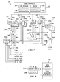
- Figure 7 illustrates a more detailed block diagram of the data storage 122 in accordance with a preferred embodiment with a RAMset cache and a two-way set associative cache.
- a cache controller 222 may control operation of the data storage 122.
- Cache controller 222 may include a plurality of status bits including, without limitation, the following four status bits: RAM_fill_mode 224, Cache_Enable 226, DM/2SA 228 and Full_RAM_base 230 as well as other bits that are not specifically shown in Figure 7.
- the two-way associative cache may be configured as a direct map and its other way configured as a RAMset.
- the two, two-way set associative cache may be configured as two additional RAMsets depending on cache control bit DM/2SA 238 and FULL_RAM_Set_base 230 as described in at least one of the documents hereinbefore mentioned.
- the preferred configuration comprises a single RAMset coupled to a standard data cache.
- the RAMset is not limited in size, nor must the RAMset have the same size as the other cache way. Therefore, if another RAMset is needed for capacity reasons, a single RAMset with a bigger size may be preferred.
- cache controller 222 couples to Full_Set_Tag registers 232 (individually referenced as registers 232a through 232c), Global_Valid bits 234 (individually referenced as bits 234a through 234c), tag memories 236 (individually referenced as tag memories 236b and 236c), valid entry bit arrays 237 (individually referenced as bit arrays 237a through 237c) and data arrays 238 (individually referenced as data arrays 238a through 238c).
- Comparators 240 (individually referenced as comparators 240a through 240c) may couple to respective Full_Set_Tag registers 232.
- Comparators 242 (individually referenced as comparators 242b and 242c) couple to respective tag memories 236.
- Output buffers 244 may couple to respective data arrays 238.
- Hit/Miss logic 246 (individually referenced as logic 246a through 246c) may couple to comparators 240, global valid bits 234, valid bits 237, RAM_fill_mode bit 224 and Cache_Enable bit 226.
- data storage 122 may be configured using the control bits 224, 226, 228 and 230.
- a line e.g., 16 bytes
- the size of the data array 238a may be different than the size of the data arrays 238b, c for the other ways of the cache.
- data arrays 238b and 238c are each 8 Kbytes in size, configured as 512 lines, with each line holding eight two-byte data values.
- Data array 238a may be 16 Kbytes in size, configured as 1024 lines, each line holding eight, two byte data values.
- the ADDR[L] signals may be used to address one line of the data array 238 and valid bit array 237 (and tag memory 236, where applicable). Accordingly, for the 1024-line first way, ADDR[L] may include 10 bits [13:4] of an address from the core.
- ADDR[L] may include 9 bits [12:4] of an address from the core.
- the ADDR[H] signals define which set is mapped to a line.
- ADDR[H] uses bits [31:14] of an address from the core for the first way and uses bits [31:13] for each of the second and third ways of the cache 130.
- the tag memories 236 and comparators 242 may be used for a 2-way set associative cache (e.g., D-cache 124 in Figure 3).
- the tag memories 236 are accessed at the low order bits of the address (ADDR[L]).
- the tag memory locations store the high order address bits of the main memory address of the information stored in a corresponding line of the data array 238. These high order address bits may be compared with the high order address bits (ADDR[H]) of the address from the core 120. If the ADDR[H] matches the contents of the tag memory at ADDR[L], a hit occurs if the valid bit associated with the low order bits indicates that the cache entry is valid.
- the data from the corresponding data array 238 at ADDR[L] may be provided to the core 120 by enabling the corresponding output buffer 244.
- data from the 2-way cache is presented to the core 120 if there is a miss in the RAMset cache.
- the operation of the 2-way set associative cache and the direct map cache may be conventional and may not be affected by the RAMset cache 126.
- Other cache techniques could also be used in place of the 2-way cache 124.
- the RAMset cache 126 preferably stores a contiguous block of main memory 106 starting at an address defined by the Full_set tag register 232 for the RAMset.
- This contiguous block of information (e.g., local variables/pointers) may be mapped to the corresponding data array 238 of the RAMset.
- only the high order bits of the starting address are stored in the Full_set_tag register 232.
- Figure 8 illustrates this mapping for a single RAMset. As shown, the contents of Full_set_tag register 232a define the starting address for a contiguous block of memory cached in data array 238a.
- a RAMset miss may occur when the high order bits of the address from the core 120 do not match the contents of the Full_set_TAG register 232 or the global valid bit is "0".
- the data storage 122 may behave like conventional, 2-way cache logic. As such, if there is a hit in the 2-way associative cache, then data is presented to the core 120 from the 2-way set associative cache. Otherwise, the data is retrieved from main memory 106, forwarded to the core and loaded into a "victim" entry of the two-way associative cache.
- a RAMset hit situation may occur when the high order bits of the address from the core 120 match the contents of the Full set TAG register 232 and the global valid bit equals "1" (the setting of the global valid bit is described in greater detail below). By default, the RAMset comparison preferably has higher priority than the other cache ways.
- a hit situation indicates that the requested data is mapped into the RAMset. If the Valid entry bit 237 corresponding to the line containing the data is set to "1", comparator 240 causes hit/miss logic 246 to generate a "hit-hit" signal because the address hit the RAMset and the data is present in the RAM set.
- logic 240 If the corresponding valid bit of the RAMset entry 237 is "0", logic 240 generates a "hit-miss" because the address hit the RAM set, but the data is not yet present in the RAM set. In this latter case, the data may be fetched from main memory 106 and loaded into the data array 238 of the RAMset. A hit in the RAMset logic takes precedence over the normal cache logic. The standard logic of the 2-way cache generates a miss when the RAMset logic generates a hit. Information can reside in both the RANset and the 2-way cache without causing any misbehavior; the duplicated cache entry in the 2-way cache will eventually be evicted by the replacement mechanism of the two-way cache because such data will not be used.
- data array 238 a,b,c When configured as a RAMset, data array 238 a,b,c can be configured as a local RAM or as a cached segment depending on the setting of a suitable configuration bit. However, even when configured as a local RAM, individual valid bits may be updated and misses do not generate accesses to the external memory.
- the Full_set_tag register 232 preferably is loaded with a start address (set_start_addr) and the RAM_fill_mode bit 224 is configured to a desired fill mode.
- the circuitry for filling the cache can be the same as that used to fill lines of the set associative cache. At least one fill mode may be implemented and is referred to as a "line-by-line" fill mode as described below. Other fill modes may be implemented if desired such as the "set fill" mode described in at least one the documents hereinbefore mentioned.
- the global valid bit 34 is set to "1" and the valid entry bits 237 are set to "0" when the Full_set_tag register 232 is loaded with the starting address.
- the data array 238 is empty (it is assumed that the Cache_Enable bit 226 is set to "1" to allow operation of the data storage 122).
- a valid entry bit 237 is selected based on the low order bits of the address.
- the Full_set_TAG register 232 may store 18 bits [31:14] of the starting address (set_start_addr).
- the address indexing each entry of the RAMset (ADDR[L]) may have 10 bits [13:4] and the data address, used to access one data value in the line, may have 3 bits [3:1] (assuming data accesses are 2 bytes).
- a line of the data array 238 (at ADDR[L]) is loaded from main memory 106 each time that a hit-miss situation occurs because (1) the comparator 240 determines a match between ADDR[H] and Set_start_addr, (2) the Global valid bit 34 is set to "1" and (3) the valid bit 237 associated with the line at ADDR[L] is "0". This situation indicates that the selected line is mapped to the RAMset, but has not yet been loaded into the RAMset's data array 238. When the line is loaded into the data array 238 from main memory 106, the valid bit 237 corresponding to the line is set to "1". This loading procedure has the same time penalty as a normal cache line load, but the entry will stay in the RAMset like a locked entry and, therefore, the processing device will not be penalized on a subsequent access.
- the contents of a RAMset can be changed simply by writing a new Set_start_addr into the Full set tag register 232. Writing to this register flushes the contents of the respective set and initiates a load process.
- the control circuitry 222 can use the same circuitry for flushing lines of the RAMset cache as is used for the set associative cache. Flushing an entire RAMset cache may be accomplished simply by writing to the appropriate Full_set_tag register 232. Similarly, the control circuitry 222 can use the same circuitry for filling lines of the RAMset cache as is used for the set associative cache.
Landscapes
- Engineering & Computer Science (AREA)
- Theoretical Computer Science (AREA)
- Software Systems (AREA)
- Physics & Mathematics (AREA)
- General Engineering & Computer Science (AREA)
- General Physics & Mathematics (AREA)
- Memory System Of A Hierarchy Structure (AREA)
Priority Applications (2)
| Application Number | Priority Date | Filing Date | Title |
|---|---|---|---|
| EP03291905A EP1387247A3 (fr) | 2002-07-31 | 2003-07-30 | Système et procédé d' empilage et desempilage automatique de variables locales Java |
| US10/632,228 US7069415B2 (en) | 2002-07-31 | 2003-07-31 | System and method to automatically stack and unstack Java local variables |
Applications Claiming Priority (3)
| Application Number | Priority Date | Filing Date | Title |
|---|---|---|---|
| US40039102P | 2002-07-31 | 2002-07-31 | |
| US400391P | 2002-07-31 | ||
| EP03291905A EP1387247A3 (fr) | 2002-07-31 | 2003-07-30 | Système et procédé d' empilage et desempilage automatique de variables locales Java |
Publications (2)
| Publication Number | Publication Date |
|---|---|
| EP1387247A2 true EP1387247A2 (fr) | 2004-02-04 |
| EP1387247A3 EP1387247A3 (fr) | 2007-12-12 |
Family
ID=38606265
Family Applications (1)
| Application Number | Title | Priority Date | Filing Date |
|---|---|---|---|
| EP03291905A Withdrawn EP1387247A3 (fr) | 2002-07-31 | 2003-07-30 | Système et procédé d' empilage et desempilage automatique de variables locales Java |
Country Status (2)
| Country | Link |
|---|---|
| US (1) | US7069415B2 (fr) |
| EP (1) | EP1387247A3 (fr) |
Cited By (2)
| Publication number | Priority date | Publication date | Assignee | Title |
|---|---|---|---|---|
| GB2418272A (en) * | 2004-09-17 | 2006-03-22 | Marconi Comm Ltd | Processor arrangement having a stack memeory |
| GB2430052A (en) * | 2005-09-07 | 2007-03-14 | Tandberg Television Asa | CPU with a buffer memory directly available to an arithmetic logic unit |
Families Citing this family (11)
| Publication number | Priority date | Publication date | Assignee | Title |
|---|---|---|---|---|
| US7478224B2 (en) * | 2005-04-15 | 2009-01-13 | Atmel Corporation | Microprocessor access of operand stack as a register file using native instructions |
| CN100361094C (zh) * | 2005-07-01 | 2008-01-09 | 华为技术有限公司 | 一种节省全局变量内存空间的方法 |
| US8190861B2 (en) * | 2006-12-04 | 2012-05-29 | Texas Instruments Incorporated | Micro-sequence based security model |
| CN103970547A (zh) * | 2014-05-28 | 2014-08-06 | 北京经纬恒润科技有限公司 | 变量生成方法和装置及数据处理方法和装置 |
| US10620955B2 (en) | 2017-09-19 | 2020-04-14 | International Business Machines Corporation | Predicting a table of contents pointer value responsive to branching to a subroutine |
| US11061575B2 (en) | 2017-09-19 | 2021-07-13 | International Business Machines Corporation | Read-only table of contents register |
| US10705973B2 (en) | 2017-09-19 | 2020-07-07 | International Business Machines Corporation | Initializing a data structure for use in predicting table of contents pointer values |
| US10896030B2 (en) * | 2017-09-19 | 2021-01-19 | International Business Machines Corporation | Code generation relating to providing table of contents pointer values |
| US10725918B2 (en) | 2017-09-19 | 2020-07-28 | International Business Machines Corporation | Table of contents cache entry having a pointer for a range of addresses |
| US10713050B2 (en) | 2017-09-19 | 2020-07-14 | International Business Machines Corporation | Replacing Table of Contents (TOC)-setting instructions in code with TOC predicting instructions |
| US10884929B2 (en) | 2017-09-19 | 2021-01-05 | International Business Machines Corporation | Set table of contents (TOC) register instruction |
Family Cites Families (8)
| Publication number | Priority date | Publication date | Assignee | Title |
|---|---|---|---|---|
| US6098089A (en) * | 1997-04-23 | 2000-08-01 | Sun Microsystems, Inc. | Generation isolation system and method for garbage collection |
| US6092152A (en) * | 1997-06-23 | 2000-07-18 | Sun Microsystems, Inc. | Method for stack-caching method frames |
| GB9907283D0 (en) * | 1999-03-31 | 1999-05-26 | Koninkl Philips Electronics Nv | Memory reclamation method |
| EP1182565B1 (fr) * | 2000-08-21 | 2012-09-05 | Texas Instruments France | Antémémoire et DMA à bit de validité global |
| EP1182562B1 (fr) * | 2000-08-21 | 2011-05-11 | Texas Instruments France | Antémémoire intelligente à préextraction de bloc interruptible |
| WO2002045385A2 (fr) * | 2000-11-20 | 2002-06-06 | Zucotto Wireless, Inc. | Procedes et dispositifs de mise en antememoire de segments de trames de methodes dans une unite de traitement a memoire de pile de faible puissance |
| US6567905B2 (en) * | 2001-01-23 | 2003-05-20 | Gemstone Systems, Inc. | Generational garbage collector with persistent object cache |
| EP1304620A1 (fr) * | 2001-10-17 | 2003-04-23 | Texas Instruments Incorporated | Antémémoire avec attribution sélective d'écriture |
-
2003
- 2003-07-30 EP EP03291905A patent/EP1387247A3/fr not_active Withdrawn
- 2003-07-31 US US10/632,228 patent/US7069415B2/en not_active Expired - Lifetime
Cited By (2)
| Publication number | Priority date | Publication date | Assignee | Title |
|---|---|---|---|---|
| GB2418272A (en) * | 2004-09-17 | 2006-03-22 | Marconi Comm Ltd | Processor arrangement having a stack memeory |
| GB2430052A (en) * | 2005-09-07 | 2007-03-14 | Tandberg Television Asa | CPU with a buffer memory directly available to an arithmetic logic unit |
Also Published As
| Publication number | Publication date |
|---|---|
| EP1387247A3 (fr) | 2007-12-12 |
| US7069415B2 (en) | 2006-06-27 |
| US20040059893A1 (en) | 2004-03-25 |
Similar Documents
| Publication | Publication Date | Title |
|---|---|---|
| US7546437B2 (en) | Memory usable in cache mode or scratch pad mode to reduce the frequency of memory accesses | |
| US20040024798A1 (en) | Conditional garbage based on monitoring to improve real time performance | |
| US7069415B2 (en) | System and method to automatically stack and unstack Java local variables | |
| US7203797B2 (en) | Memory management of local variables | |
| EP1387252B1 (fr) | Code préfixe pour indiquer la présence de commandes de système | |
| US7330937B2 (en) | Management of stack-based memory usage in a processor | |
| EP1387275B1 (fr) | Gestion de mémoire de variables locales lors d'un changement de contexte | |
| EP1387250B1 (fr) | Processeur à jeux d'instructions et à modes de decodage multiples | |
| EP1387253B1 (fr) | Traduction dynamique et exécution d'instructions dans un processeur | |
| US8429383B2 (en) | Multi-processor computing system having a JAVA stack machine and a RISC-based processor | |
| EP1387248B1 (fr) | Processeur muni d'une mémoire d'empilement partagée | |
| EP1387251B1 (fr) | Instruction de copiage de données d'un stockage de piles |
Legal Events
| Date | Code | Title | Description |
|---|---|---|---|
| PUAI | Public reference made under article 153(3) epc to a published international application that has entered the european phase |
Free format text: ORIGINAL CODE: 0009012 |
|
| AK | Designated contracting states |
Kind code of ref document: A2 Designated state(s): AT BE BG CH CY CZ DE DK EE ES FI FR GB GR HU IE IT LI LU MC NL PT RO SE SI SK TR |
|
| AX | Request for extension of the european patent |
Extension state: AL LT LV MK |
|
| PUAL | Search report despatched |
Free format text: ORIGINAL CODE: 0009013 |
|
| RIC1 | Information provided on ipc code assigned before grant |
Ipc: G06F 12/08 20060101ALI20031126BHEP Ipc: G06F 9/42 20060101AFI20071026BHEP |
|
| AK | Designated contracting states |
Kind code of ref document: A3 Designated state(s): AT BE BG CH CY CZ DE DK EE ES FI FR GB GR HU IE IT LI LU MC NL PT RO SE SI SK TR |
|
| AX | Request for extension of the european patent |
Extension state: AL LT LV MK |
|
| 17P | Request for examination filed |
Effective date: 20080612 |
|
| AKX | Designation fees paid |
Designated state(s): DE FR GB |
|
| RAP1 | Party data changed (applicant data changed or rights of an application transferred) |
Owner name: TEXAS INSTRUMENTS FRANCE Owner name: TEXAS INSTRUMENTS INC. |
|
| RBV | Designated contracting states (corrected) |
Designated state(s): DE FR GB NL |
|
| 17Q | First examination report despatched |
Effective date: 20090216 |
|
| STAA | Information on the status of an ep patent application or granted ep patent |
Free format text: STATUS: THE APPLICATION IS DEEMED TO BE WITHDRAWN |
|
| 18D | Application deemed to be withdrawn |
Effective date: 20101207 |