EP1390984B1 - Floating-gate-speicherbaustein, der zusammengesetztes molekularmaterial verwendet - Google Patents
Floating-gate-speicherbaustein, der zusammengesetztes molekularmaterial verwendet Download PDFInfo
- Publication number
- EP1390984B1 EP1390984B1 EP02769351A EP02769351A EP1390984B1 EP 1390984 B1 EP1390984 B1 EP 1390984B1 EP 02769351 A EP02769351 A EP 02769351A EP 02769351 A EP02769351 A EP 02769351A EP 1390984 B1 EP1390984 B1 EP 1390984B1
- Authority
- EP
- European Patent Office
- Prior art keywords
- floating gate
- insulating layer
- state
- molecular
- resistivity
- Prior art date
- Legal status (The legal status is an assumption and is not a legal conclusion. Google has not performed a legal analysis and makes no representation as to the accuracy of the status listed.)
- Expired - Lifetime
Links
- 239000002131 composite material Substances 0.000 title description 9
- 239000000463 material Substances 0.000 title description 8
- 239000011159 matrix material Substances 0.000 claims abstract description 22
- 230000005684 electric field Effects 0.000 claims abstract description 15
- 230000000717 retained effect Effects 0.000 claims abstract description 4
- -1 polyparaphenylene Polymers 0.000 claims description 8
- 150000001875 compounds Chemical class 0.000 claims description 7
- 239000000758 substrate Substances 0.000 claims description 7
- 230000004044 response Effects 0.000 claims description 5
- YMWLPMGFZYFLRP-UHFFFAOYSA-N 2-(4,5-dimethyl-1,3-diselenol-2-ylidene)-4,5-dimethyl-1,3-diselenole Chemical compound [Se]1C(C)=C(C)[Se]C1=C1[Se]C(C)=C(C)[Se]1 YMWLPMGFZYFLRP-UHFFFAOYSA-N 0.000 claims description 2
- 125000003118 aryl group Chemical group 0.000 claims description 2
- 125000000623 heterocyclic group Chemical group 0.000 claims description 2
- 229910010272 inorganic material Inorganic materials 0.000 claims description 2
- 229910052723 transition metal Inorganic materials 0.000 claims description 2
- 229920000265 Polyparaphenylene Polymers 0.000 claims 1
- 239000011147 inorganic material Substances 0.000 claims 1
- 229920000767 polyaniline Polymers 0.000 claims 1
- 229920000128 polypyrrole Polymers 0.000 claims 1
- 229920000123 polythiophene Polymers 0.000 claims 1
- 230000008859 change Effects 0.000 abstract description 5
- 230000014759 maintenance of location Effects 0.000 description 7
- FAPWRFPIFSIZLT-UHFFFAOYSA-M Sodium chloride Chemical compound [Na+].[Cl-] FAPWRFPIFSIZLT-UHFFFAOYSA-M 0.000 description 6
- 230000007704 transition Effects 0.000 description 6
- 239000012212 insulator Substances 0.000 description 4
- 239000011780 sodium chloride Substances 0.000 description 3
- 230000003068 static effect Effects 0.000 description 3
- VYPSYNLAJGMNEJ-UHFFFAOYSA-N Silicium dioxide Chemical compound O=[Si]=O VYPSYNLAJGMNEJ-UHFFFAOYSA-N 0.000 description 2
- 150000001768 cations Chemical class 0.000 description 2
- 239000004020 conductor Substances 0.000 description 2
- 229920000547 conjugated polymer Polymers 0.000 description 2
- 230000021615 conjugation Effects 0.000 description 2
- 239000013078 crystal Substances 0.000 description 2
- 238000013500 data storage Methods 0.000 description 2
- 230000007423 decrease Effects 0.000 description 2
- 239000003989 dielectric material Substances 0.000 description 2
- 230000001747 exhibiting effect Effects 0.000 description 2
- 150000002500 ions Chemical class 0.000 description 2
- 230000007246 mechanism Effects 0.000 description 2
- 229920001197 polyacetylene Polymers 0.000 description 2
- 229920000642 polymer Polymers 0.000 description 2
- 239000004065 semiconductor Substances 0.000 description 2
- PCCVSPMFGIFTHU-UHFFFAOYSA-N tetracyanoquinodimethane Chemical compound N#CC(C#N)=C1C=CC(=C(C#N)C#N)C=C1 PCCVSPMFGIFTHU-UHFFFAOYSA-N 0.000 description 2
- DGAQECJNVWCQMB-PUAWFVPOSA-M Ilexoside XXIX Chemical compound C[C@@H]1CC[C@@]2(CC[C@@]3(C(=CC[C@H]4[C@]3(CC[C@@H]5[C@@]4(CC[C@@H](C5(C)C)OS(=O)(=O)[O-])C)C)[C@@H]2[C@]1(C)O)C)C(=O)O[C@H]6[C@@H]([C@H]([C@@H]([C@H](O6)CO)O)O)O.[Na+] DGAQECJNVWCQMB-PUAWFVPOSA-M 0.000 description 1
- 229910020050 NbSe3 Inorganic materials 0.000 description 1
- 229910005171 Si3O4 Inorganic materials 0.000 description 1
- XUIMIQQOPSSXEZ-UHFFFAOYSA-N Silicon Chemical compound [Si] XUIMIQQOPSSXEZ-UHFFFAOYSA-N 0.000 description 1
- 125000002015 acyclic group Chemical group 0.000 description 1
- HSFWRNGVRCDJHI-UHFFFAOYSA-N alpha-acetylene Natural products C#C HSFWRNGVRCDJHI-UHFFFAOYSA-N 0.000 description 1
- 150000001450 anions Chemical class 0.000 description 1
- 238000013459 approach Methods 0.000 description 1
- 230000004888 barrier function Effects 0.000 description 1
- 230000015572 biosynthetic process Effects 0.000 description 1
- 230000003915 cell function Effects 0.000 description 1
- 239000000460 chlorine Substances 0.000 description 1
- 229910052801 chlorine Inorganic materials 0.000 description 1
- 229910052681 coesite Inorganic materials 0.000 description 1
- 239000002322 conducting polymer Substances 0.000 description 1
- 229920001940 conductive polymer Polymers 0.000 description 1
- 229910052906 cristobalite Inorganic materials 0.000 description 1
- 230000003247 decreasing effect Effects 0.000 description 1
- 230000001066 destructive effect Effects 0.000 description 1
- 239000007772 electrode material Substances 0.000 description 1
- 238000002474 experimental method Methods 0.000 description 1
- 150000002484 inorganic compounds Chemical class 0.000 description 1
- 229920002521 macromolecule Polymers 0.000 description 1
- 229910052751 metal Inorganic materials 0.000 description 1
- 239000002184 metal Substances 0.000 description 1
- 238000000034 method Methods 0.000 description 1
- 238000005442 molecular electronic Methods 0.000 description 1
- 239000000615 nonconductor Substances 0.000 description 1
- 230000008520 organization Effects 0.000 description 1
- 150000004032 porphyrins Chemical class 0.000 description 1
- 230000008569 process Effects 0.000 description 1
- 150000003839 salts Chemical class 0.000 description 1
- 238000000926 separation method Methods 0.000 description 1
- 229910052710 silicon Inorganic materials 0.000 description 1
- 239000010703 silicon Substances 0.000 description 1
- 239000000377 silicon dioxide Substances 0.000 description 1
- 229910052708 sodium Inorganic materials 0.000 description 1
- 239000011734 sodium Substances 0.000 description 1
- 159000000000 sodium salts Chemical class 0.000 description 1
- 229910052682 stishovite Inorganic materials 0.000 description 1
- 239000010409 thin film Substances 0.000 description 1
- 229910052905 tridymite Inorganic materials 0.000 description 1
Images


Classifications
-
- G—PHYSICS
- G11—INFORMATION STORAGE
- G11C—STATIC STORES
- G11C13/00—Digital stores characterised by the use of storage elements not covered by groups G11C11/00, G11C23/00, or G11C25/00
- G11C13/0002—Digital stores characterised by the use of storage elements not covered by groups G11C11/00, G11C23/00, or G11C25/00 using resistive RAM [RRAM] elements
- G11C13/0009—RRAM elements whose operation depends upon chemical change
-
- H—ELECTRICITY
- H10—SEMICONDUCTOR DEVICES; ELECTRIC SOLID-STATE DEVICES NOT OTHERWISE PROVIDED FOR
- H10D—INORGANIC ELECTRIC SEMICONDUCTOR DEVICES
- H10D30/00—Field-effect transistors [FET]
- H10D30/60—Insulated-gate field-effect transistors [IGFET]
- H10D30/68—Floating-gate IGFETs
-
- B—PERFORMING OPERATIONS; TRANSPORTING
- B82—NANOTECHNOLOGY
- B82Y—SPECIFIC USES OR APPLICATIONS OF NANOSTRUCTURES; MEASUREMENT OR ANALYSIS OF NANOSTRUCTURES; MANUFACTURE OR TREATMENT OF NANOSTRUCTURES
- B82Y10/00—Nanotechnology for information processing, storage or transmission, e.g. quantum computing or single electron logic
-
- G—PHYSICS
- G11—INFORMATION STORAGE
- G11C—STATIC STORES
- G11C13/00—Digital stores characterised by the use of storage elements not covered by groups G11C11/00, G11C23/00, or G11C25/00
- G11C13/0002—Digital stores characterised by the use of storage elements not covered by groups G11C11/00, G11C23/00, or G11C25/00 using resistive RAM [RRAM] elements
- G11C13/0009—RRAM elements whose operation depends upon chemical change
- G11C13/0014—RRAM elements whose operation depends upon chemical change comprising cells based on organic memory material
-
- H—ELECTRICITY
- H10—SEMICONDUCTOR DEVICES; ELECTRIC SOLID-STATE DEVICES NOT OTHERWISE PROVIDED FOR
- H10D—INORGANIC ELECTRIC SEMICONDUCTOR DEVICES
- H10D30/00—Field-effect transistors [FET]
- H10D30/60—Insulated-gate field-effect transistors [IGFET]
- H10D30/68—Floating-gate IGFETs
- H10D30/681—Floating-gate IGFETs having only two programming levels
-
- H—ELECTRICITY
- H10—SEMICONDUCTOR DEVICES; ELECTRIC SOLID-STATE DEVICES NOT OTHERWISE PROVIDED FOR
- H10D—INORGANIC ELECTRIC SEMICONDUCTOR DEVICES
- H10D64/00—Electrodes of devices having potential barriers
- H10D64/60—Electrodes characterised by their materials
- H10D64/66—Electrodes having a conductor capacitively coupled to a semiconductor by an insulator, e.g. MIS electrodes
- H10D64/68—Electrodes having a conductor capacitively coupled to a semiconductor by an insulator, e.g. MIS electrodes characterised by the insulator, e.g. by the gate insulator
-
- G—PHYSICS
- G11—INFORMATION STORAGE
- G11C—STATIC STORES
- G11C2213/00—Indexing scheme relating to G11C13/00 for features not covered by this group
- G11C2213/10—Resistive cells; Technology aspects
- G11C2213/13—Dissociation, i.e. using memory material including molecules which, during a write operation, are dissociated in ions which migrate further in the memory material
-
- G—PHYSICS
- G11—INFORMATION STORAGE
- G11C—STATIC STORES
- G11C2213/00—Indexing scheme relating to G11C13/00 for features not covered by this group
- G11C2213/10—Resistive cells; Technology aspects
- G11C2213/15—Current-voltage curve
Definitions
- the invention relates to a floating gate memory cell for data storage applications, and more particularly, to a floating gate memory device having a variable resistance dielectric as a gate insulator.
- DRAM Dynamic random access memory
- SRAM Static random access memory
- SRAM stores data in a bistable flip-flop, commonly consisting of cross-coupled inverters. It is called “static” because it will retain a value as long as power is supplied. It is still volatile, i.e. it will lose its contents when the power is switched off, in contrast to ROM.
- SRAM is usually faster than DRAM, but each bit requires several transistors (about six), so that a lesser number of bits of SRAM fit in the same area as compared to DRAM.
- Nonvolatile memory devices have been extensively used in integrated circuits, such as the electrically alterable read-only memory (EAOM), the erasable-programmable read-only memory (PROM), and the nonvolatile random-access memory (NVRAM).
- EAOM electrically alterable read-only memory
- PROM erasable-programmable read-only memory
- NVRAM nonvolatile random-access memory
- EP 0 727 822 discloses a memory apparatus on a semiconductor substrate including first and second electrodes, wherein a resistance value between the first and second electrodes are arranged to advantageously change from a high to a low resistance state.
- a floating gate memory device comprising a substrate and a first insulating layer on the substrate.
- a floating gate is provided on the first insulating layer, and a second insulating layer is on the floating gate.
- a control gate is formed on the second insulating layer.
- At least one of the first or the second insulating layers has a controllably variable resistivity wherein the resistivity can be changed in response to the application of an electric field to switch the resistivity from a highly resistive state, where charge is retained by the floating gate, to a lower resistivity state, where the charge stored on the floating gate can be drained off to the control gate and wherein the resistivity can be restored to the highly resistive state in response to the application of an electric field of reverse polarity.
- At least one of the first and second insulating layers consists of a molecular matrix with ionic complexes distributed through the molecular matrix and wherein the ionic complexes are dissociable in the molecular matrix under the influence of an applied electronic field.
- At least one of the first and second insulating layers comprises a material switchable between low and high conductivity states in response to an applied electric field, and wherein the material is a molecular matrix with ionic complexes distributed in the molecular matrix, the ionic complexes being dissociable in the molecular matrix under the influence of an applied electric field.
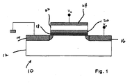
- Fig. 1 shows a nonvolatile memory device that is a floating gate transistor constructed in accordance with an embodiment of the present invention
- Fig. 2a-d show a molecular composite material between two electrodes in various operational states according to a current theoretical understanding of the invention
- Fig. 3 shows a voltage-current characteristic for write and erase operations of the memory device of the present invention.
- Fig. 4 shows the dependence on writing pulse critical amplitude on writing pulse time.
- a floating gate transistor may be considered to be a modified MOSFET transistor with a floating conductive pad embedded in the dielectric that insulates the gate from the source/drain. Because of the very high resistivity of commonly used dielectrics, such as SiO 2 and Si 3 O 4 , any electric charge deposited on the floating gate will remain there during the retention time of the device, which can be years. However, it is difficult to discharge the floating gate simply by applying a reverse external electric field because of the large electrical resistance of the tunnel barrier in the reverse direction. For this reason, the conductivity of the dielectric is typically enhanced by illuminating the dielectric with UV light.
- the present invention provides a structure that avoids the need for UV light.
- the present invention address and solves problems related to the control and structure of a floating gate memory device.
- the present invention provides for a floating gate memory device that has an insulating layer that acts to either electrically insulate the floating gate from a control gate, or has an increased conductivity to allow for a rapid discharge of the floating gate charge.
- a floating gate transistor having an insulating layer between the control gate and the floating gate that comprises a composite material that exhibits structural electronic instability in one dimension and enables static and dynamic control over the conductivity of the composite material.
- a molecular matrix is employed with ionic complexes in the matrix. Under the application of an electric field, the ionic complexes dissociate controllably to change the electrical conductivity of the insulating layer.
- FIG. 1 depicts an exemplary embodiment of the floating gate memory device constructed in accordance with present invention.
- the floating gate memory device includes substrate 12 in which are formed source and drain regions 14, 16, respectively.
- a first insulator 18 is formed on the substrate 10 and spans the source and drain regions 14, 16.
- a floating gate 20 formed of conductive material, is formed on the first insulating layer 18.
- a second insulating layer 22 is formed on the floating gate 20, followed by the formation of gate electrode 24 on the second insulating layer 22.
- the gate electrode 24 and the drain region 16 are depicted as being connected to voltages Vg and V d , respectively.
- the gate electrode 24, like the floating gate 20, comprises a conductive material.
- At least one of the two dielectric layers 18, 22 depicted in Fig. 1 comprise a one-dimensional molecular system exhibiting a transition from a low electrical conductivity to a high electrical conductivity and vice versa. This transition is typically manifested by an S-shaped (reentrant) voltage-current characteristic with metastable or stable memory.
- the impedance of such memory cells can be between ⁇ 10 M ⁇ and ⁇ 100 ⁇ for example, depending on the switching condition. Examples of such molecular systems are systems with a low dimensionality exhibiting a so-called Peierls transition.
- insulating layers 18, 22 A number of different materials may be used as the insulating layers 18, 22. Exemplary materials are described in more detail below, but are also discussed in an article by Yu H. Krieger, entitled “Structural Instability of One-Dimensional Systems as a Physical Principle Underlying the Functioning of Molecular Electronic Devices", Journal of Structural Chemistry, Vol. 40, No. 4, 1999 (Yu H. Krieger), expressly incorporated by reference herein.
- Polyconjugated systems primarily involve polyvinylenes, i.e., polymers with an acyclic conjugation system, in which the one-dimensional character of structure is dictated by the mechanism of conjugation in linear macromolecules.
- Polyacetylene is a classical representative of this class of polymers. Its electronic structure is a prototype for many other conjugated polymers.
- molecular compounds are formed from aromatic and heterocyclic molecules which possess high electric conductivity due to ⁇ -bonds between molecules. Such molecular systems are called ⁇ -complexes or charge transfer complexes, with those systems whose structure involves isolated one-dimensional columns or strands possessing pronounced electro-physical properties of interest for switching and memory applications.
- Molecular charge transfer complexes are donor-acceptor systems formed from two molecules: one possessing donor and another acceptor properties.
- TCNQ tetra-cyano-quino-dimethane
- TCNQ tetra-cyano-quino-dimethane
- the cations are dynamically disordered. It involves molecular compounds having the general formula (TMTSF) 2 X. Transition metal salts of K 2 Pt(CN) 4 Br 0.3 x 3H 2 O (KCP) type are also the typical representatives of mixed-valence quasi-one-dimensional complexes, as are phthalocyanines and porphyrins. Moreover, pure inorganic compounds, such as NbSe 3 , are also interesting examples of compounds with quasi-one-dimensional structure.
- the molecular composite includes a quasi-one-dimensional, or at least structurally and electrically anisotropic, molecular matrix, wherein ionic complexes are distributed in the matrix.
- Polyconjugated compounds such as the exemplary quasi-one-dimensional systems described above, for example, polyphenylacetylene, can be used as the anisotropic molecular matrix.
- the ionic complex can be a salt, such as sodium chloride (NaCl), or any other material that can dissociate in an applied electric field.
- the exemplary anisotropic molecular matrix is depicted in Figs. 2 a-d as comprising an assembly of chain-like molecules oriented perpendicular to the electrode surfaces. However, other orientations of those molecules or of anisotropic "channels" are possible as long as a charge separation of the type depicted in Figs. 2 a-d is enabled.
- Electric switching in the molecular thin films depicted in Figs. 2a-d is characterized by the existence of two stable states, a high impedance state ("off” state) and a low impedance state ("on” state).
- the impedance of this "off' state is usually more than ⁇ 10 M ⁇ ., for example. Switching from the "off" state to the "on” state occurs when an applied electric field exceeds a threshold value.
- the impedance of this "on” state can be less than ⁇ 100 ⁇ ., for example.
- a transition from "on” state back to the "off' state can take place by reversing the polarity of the electric field.
- the metastable mode of the memory cell function is characterized by the low P W and P ER value (0.1-0.5V), high impedance of the "ON" state (wide region, about 1k ⁇ - 1M ⁇ ), short switching time (less than 1 ⁇ s), and short retention time between about 10 s or several hours.
- the stable mode of the memory cell operation shows the high Pw and P ER value (3-10V), low impedance of the "ON" state (less than 100 ⁇ ), long switching time (1 ms and more) and long storage time (between several months and years).
- Fig. 2a illustrates the "off" state, where the electrical conductivity is essentially zero, assuming that the anisotropic molecular matrix itself is a good electrical insulator.
- an external electric field E is applied, as indicated in Fig. 2b , the sodium salt dissociates into sodium and chlorine ions, and the ions are displaced from their original position in the anisotropic molecular matrix, resulting in an increase in the electrical conductivity to the metastable "on” state.
- the ions become more strongly separated ( Fig. 2c ), accompanied by a still further increase in the conductivity of the "on” state to the above-described stable state .
- the anions and cations accumulate at the electrodes ( Fig. 2d ), resulting in a sharp decrease in the electrical conductivity due to the absence of mobile charges ("off" state).
- the electrode material can be, for example, a metal, such as Al or Cu, ITO, a semiconductor or a conducting polymer.
- the transition from the "off" state depicted in Fig. 2a to the "on” state depicted in Fig. 2b requires application of an external voltage of approximately 3-5 V for a time period of approximately 10-100 ns.
- the transition from the "off" state depicted in Fig. 2a to the "on” state depicted in Fig. 2c having a higher electrical conductivity and lounger retention time is achieved by applying an external voltage of approximately 3-5 V for a time period of approximately 300 ns - 1 ⁇ s.
- a molecular composite comprising polyphenylacetylene and -5-7% NaCl as the ionic complex are described in these figures as an exemplary embodiment
- variable conductivity gate insulator with a floating gate transistor, replacing at least one of the traditional dielectrics (e.g., insulating layer 22), the conductivity is switched between a low conductivity state, where charge is retained by the floating gate, and a higher conductivity state, where the charge stored on the floating gate 20 can be drained off to the gate electrode 24.
- the floating gate 20 can thereafter be restored to its original state, i.e., isolated from the gate 24, by applying a reverse potential between the source/drain 14, 16 and the gate electrode 24.
- the current-voltage (I-V) characteristic of a floating gate transistor as it applies to the state of the composite material forming, for example, insulating layer 22, is shown in Fig. 3 .
- the positive voltage applied to the gate electrode with respect to the ground will be referred to as write voltage (in pulsed experiments, as write pulse) (P w ), which renders the insulating layer 22 conductive, and the negative voltage, which restores the insulating properties of insulating layer 22, as erase voltage (or erase pulse) (P ER ), respectively.
- Fig. 3 shows a typical I-V curve for write (positive applied voltage) and erase operation (negative applied voltage).
- the device is in the "off' state, until the applied voltage reaches a critical value of approximately 0.3 V.
- the critical voltage of 0.3V the critical voltage of 0.3V
- the memory cell 10 approaches zero resistance, with the voltage across the cell dropping to a very small value and the current increasing to more than 120 ⁇ A, with the cell attaining the "on” state.
- the cell remains in the "on” state until a negative voltage is applied, which in the present example is approximately -1 V.
- the parameter (voltage, pulse duration) used"for the erase operation depend on the characteristic values of the "on” state of the device.
- the pulse duration of a write pulse required to change the conductivity of the insulating layer 22 its related to the amplitude of the write pulse For example, insulating layer 22 may be switched from the "off' state to the "on" state by applying a pulse of 4 V for 10 ⁇ s, whereas a pulse duration of more than 1 ms may be required when writing with a voltage of approximately 1 V. Accordingly, the speed with which the conductivity of the insulating layer 22 of the device 10 changes can be adapted to specific applications.
- the present invention thus provides an easily erasable floating gate transistor memory chip for systems, employing molecular memory cells.
- the electronic circuitry of the erasable floating gate transistor memory chip can be based on that of well-developed DRAM chips.
- the circuit can work as either SRAM or DRAM.
Landscapes
- Engineering & Computer Science (AREA)
- Chemical & Material Sciences (AREA)
- Nanotechnology (AREA)
- Physics & Mathematics (AREA)
- Mathematical Physics (AREA)
- Theoretical Computer Science (AREA)
- Crystallography & Structural Chemistry (AREA)
- Semiconductor Memories (AREA)
- Non-Volatile Memory (AREA)
Claims (4)
- Speicherbauelement mit Gate mit einstellbarem Potential, mit:einem Substrat (10);einer ersten isolierenden Schicht (18) auf dem Substrat (10);einem Gate mit frei einstellbarem Potential (20) auf der ersten isolierenden Schicht (18);einer zweiten isolierenden Schicht (22) auf dem Gate mit frei einstellbarem Potential (20); undeinem Steuergate (24) auf der zweiten isolierenden Schicht (22);wobei die erste isolierende Schicht (18) und/oder die zweite isolierende Schicht (22) einen steuerbar variablen Widerstand besitzt, der sich in Reaktion auf das Anlegen eines elektrischen Feldes ändert, um den Widerstand von einem Zustand mit hohem Widerstandswert, in welchem Ladung in dem Gate mit frei einstellbarem Potential gehalten wird, in einen Zustand mit geringem Widerstandswert umzuschalten, in welchem die in dem Gate mit frei einstellbarem Potential gespeicherte Ladung an das Steuergate abgeführt wird und wobei der Zustand mit hohem Widerstandswert in Reaktion auf das Anlegen eines elektrischen Feldes mit umgekehrter Polarität wieder hergestellt werden kann.
- Bauelement nach Anspruch 1, wobei die erste isolierende Schicht (18) und/oder die zweite isolierende Schicht (22) eine molekulare Matrix aufweist, wobei die erste isolierende Schicht (18) und/oder die zweite isolierende Schicht (22) ferner ionische Komplexe enthält, die in der molekularen Matrix verteilt sind und wobei die ionischen Komplexe unter dem Einfluss eines angelegten elektrischen Feldes in der molekularen Matrix dissoziierbar sind.
- Bauelement nach Anspruch 2, wobei die molekulare Matrix eine polykonjugierte Verbindung aufweist und wobei die polykonjugierte Verbindung eine der folgenden ist: Polyparaphenylen, Polyvenylvenylen, Polyanilin, Polythiophen oder Polypyrol.
- Bauelement nach Anspruch 2, wobei die molekulare Matrix eines der folgenden Bestandteile aufweist: ein aromatisches Molekül, ein heterozyklisches Molekül,
einen quasi-eindimensionalen Komplex,
ein anisotropes organisches Material,
eine Molekularverbindung aus (TMTSF)2X,
ein Übergangsmetallsalz der Art K2Pt(CN)4Br0,3x3H2O (KCP).
Applications Claiming Priority (3)
| Application Number | Priority Date | Filing Date | Title |
|---|---|---|---|
| US28909101P | 2001-05-07 | 2001-05-07 | |
| US289091P | 2001-05-07 | ||
| PCT/US2002/014237 WO2002091476A1 (en) | 2001-05-07 | 2002-05-07 | Floating gate memory device using composite molecular material |
Publications (2)
| Publication Number | Publication Date |
|---|---|
| EP1390984A1 EP1390984A1 (de) | 2004-02-25 |
| EP1390984B1 true EP1390984B1 (de) | 2009-08-26 |
Family
ID=23110014
Family Applications (1)
| Application Number | Title | Priority Date | Filing Date |
|---|---|---|---|
| EP02769351A Expired - Lifetime EP1390984B1 (de) | 2001-05-07 | 2002-05-07 | Floating-gate-speicherbaustein, der zusammengesetztes molekularmaterial verwendet |
Country Status (7)
| Country | Link |
|---|---|
| US (1) | US6627944B2 (de) |
| EP (1) | EP1390984B1 (de) |
| JP (1) | JP4514016B2 (de) |
| KR (1) | KR100885276B1 (de) |
| CN (1) | CN1276518C (de) |
| DE (1) | DE60233486D1 (de) |
| WO (1) | WO2002091476A1 (de) |
Families Citing this family (32)
| Publication number | Priority date | Publication date | Assignee | Title |
|---|---|---|---|---|
| US6859548B2 (en) | 1996-09-25 | 2005-02-22 | Kabushiki Kaisha Toshiba | Ultrasonic picture processing method and ultrasonic picture processing apparatus |
| EP1390984B1 (de) | 2001-05-07 | 2009-08-26 | Advanced Micro Devices, Inc. | Floating-gate-speicherbaustein, der zusammengesetztes molekularmaterial verwendet |
| WO2002091496A2 (en) | 2001-05-07 | 2002-11-14 | Advanced Micro Devices, Inc. | Reversible field-programmable electric interconnects |
| WO2002091385A1 (en) | 2001-05-07 | 2002-11-14 | Advanced Micro Devices, Inc. | Molecular memory cell |
| CN100403450C (zh) * | 2001-05-07 | 2008-07-16 | 先进微装置公司 | 具有自组装聚合物薄膜的内存装置及其制造方法 |
| CN100367528C (zh) | 2001-05-07 | 2008-02-06 | 先进微装置公司 | 具储存效应的开关装置 |
| AU2002340793A1 (en) * | 2001-05-07 | 2002-11-18 | Coatue Corporation | Molecular memory device |
| US6768157B2 (en) * | 2001-08-13 | 2004-07-27 | Advanced Micro Devices, Inc. | Memory device |
| US6858481B2 (en) * | 2001-08-13 | 2005-02-22 | Advanced Micro Devices, Inc. | Memory device with active and passive layers |
| US6806526B2 (en) | 2001-08-13 | 2004-10-19 | Advanced Micro Devices, Inc. | Memory device |
| US6838720B2 (en) | 2001-08-13 | 2005-01-04 | Advanced Micro Devices, Inc. | Memory device with active passive layers |
| CN100419906C (zh) | 2001-08-13 | 2008-09-17 | 先进微装置公司 | 存储器单元 |
| DE10212926A1 (de) * | 2002-03-22 | 2003-10-16 | Infineon Technologies Ag | Halbleiterspeicherzelle und Halbleiterspeichereinrichtung |
| US7012276B2 (en) * | 2002-09-17 | 2006-03-14 | Advanced Micro Devices, Inc. | Organic thin film Zener diodes |
| US6922350B2 (en) * | 2002-09-27 | 2005-07-26 | Intel Corporation | Reducing the effect of write disturbs in polymer memories |
| US7049153B2 (en) * | 2003-04-23 | 2006-05-23 | Micron Technology, Inc. | Polymer-based ferroelectric memory |
| US6903361B2 (en) | 2003-09-17 | 2005-06-07 | Micron Technology, Inc. | Non-volatile memory structure |
| US6916696B1 (en) | 2003-11-20 | 2005-07-12 | Advanced Micro Devices, Inc. | Method for manufacturing a memory element |
| US20050212022A1 (en) * | 2004-03-24 | 2005-09-29 | Greer Edward C | Memory cell having an electric field programmable storage element, and method of operating same |
| KR100838931B1 (ko) * | 2004-05-18 | 2008-06-16 | 휴렛-팩커드 디벨롭먼트 컴퍼니, 엘 피 | 전기장에 의해 유도되는 분자내 전하이동, 분자간 전하이동, 또는 분자와 전극간 전하이동을 통해 전자 스위칭을 발생시키는 물질 조성물 |
| US20050274609A1 (en) * | 2004-05-18 | 2005-12-15 | Yong Chen | Composition of matter which results in electronic switching through intra- or inter- molecular charge transfer, or charge transfer between molecules and electrodes induced by an electrical field |
| DE102004031135A1 (de) * | 2004-06-28 | 2006-01-19 | Infineon Technologies Ag | Resistives Halbleiterelement basierend auf einem Festkörperionenleiter |
| US20070009821A1 (en) * | 2005-07-08 | 2007-01-11 | Charlotte Cutler | Devices containing multi-bit data |
| KR100744566B1 (ko) * | 2006-09-08 | 2007-08-01 | 한국전자통신연구원 | 금속산화물을 이용한 게이트 스택, 이를 포함하는트랜지스터 일체형 메모리 소자 및 그 메모리소자의구동방법 |
| US7915603B2 (en) * | 2006-10-27 | 2011-03-29 | Qimonda Ag | Modifiable gate stack memory element |
| KR100890212B1 (ko) * | 2007-11-23 | 2009-03-25 | 고려대학교 산학협력단 | 비휘발성 메모리 소자 및 그 제조 방법 |
| TWI466271B (zh) * | 2010-07-05 | 2014-12-21 | Macronix Int Co Ltd | 具有可調整閘極電阻值之電晶體及具有可調整閘極電阻值之電晶體之半導體元件 |
| CN102339846B (zh) * | 2010-07-19 | 2015-10-07 | 旺宏电子股份有限公司 | 具有可调整栅极电阻值的晶体管的半导体存储器元件 |
| US8675381B2 (en) | 2010-07-20 | 2014-03-18 | Macronix International Co., Ltd. | Transistor having an adjustable gate resistance and semiconductor device comprising the same |
| KR101463782B1 (ko) | 2011-04-06 | 2014-11-21 | 고려대학교 산학협력단 | 문턱전압 스위칭 물질을 이용한 비휘발성 메모리 소자 및 그 제조 방법 |
| US9767407B2 (en) | 2015-09-18 | 2017-09-19 | Samsung Electronics Co., Ltd. | Weighting device, neural network, and operating method of the weighting device |
| WO2018009175A1 (en) * | 2016-07-06 | 2018-01-11 | Intel Corporation | High speed single transistor non-volatile memory cell |
Family Cites Families (99)
| Publication number | Priority date | Publication date | Assignee | Title |
|---|---|---|---|---|
| JPS5012598B1 (de) | 1970-04-02 | 1975-05-13 | ||
| US3810127A (en) | 1970-06-23 | 1974-05-07 | Intel Corp | Programmable circuit {13 {11 the method of programming thereof and the devices so programmed |
| JPS5589980A (en) | 1978-11-27 | 1980-07-08 | Nec Corp | Semiconductor memory unit |
| US4267558A (en) * | 1979-01-05 | 1981-05-12 | Texas Instruments Incorporated | Electrically erasable memory with self-limiting erase |
| US4652894A (en) | 1980-03-14 | 1987-03-24 | The Johns Hopkins University | Electrical organic thin film switching device switching between detectably different oxidation states |
| US4371883A (en) | 1980-03-14 | 1983-02-01 | The Johns Hopkins University | Current controlled bistable electrical organic thin film switching device |
| JPS5864068A (ja) | 1981-10-14 | 1983-04-16 | Agency Of Ind Science & Technol | 不揮発性半導体メモリの書き込み方法 |
| US4677742A (en) | 1983-01-18 | 1987-07-07 | Energy Conversion Devices, Inc. | Electronic matrix arrays and method for making the same |
| GB2160049B (en) | 1984-05-28 | 1987-06-03 | Suwa Seikosha Kk | A non-volatile memory circuit |
| US5034192A (en) | 1984-11-23 | 1991-07-23 | Massachusetts Institute Of Technology | Molecule-based microelectronic devices |
| US4631562A (en) | 1985-05-31 | 1986-12-23 | Rca Corporation | Zener diode structure |
| DE3602887A1 (de) | 1986-01-31 | 1987-08-06 | Bayer Ag | Nichtfluechtiger elektronischer speicher |
| US4727514A (en) | 1986-02-11 | 1988-02-23 | Texas Instruments Incorporated | Programmable memory with memory cells programmed by addressing |
| US4834911A (en) | 1986-08-25 | 1989-05-30 | Electro-Organic Company | Intrinsically conductive and semiconductive polymers, products formed with such polymers and methods of forming same |
| DE3751376T2 (de) | 1986-10-13 | 1995-11-16 | Canon Kk | Schaltungselement. |
| JPH01100788A (ja) | 1987-10-13 | 1989-04-19 | Hitachi Ltd | 半導体集積回路装置 |
| US4839700A (en) | 1987-12-16 | 1989-06-13 | California Institute Of Technology | Solid-state non-volatile electronically programmable reversible variable resistance device |
| US5440518A (en) | 1991-06-12 | 1995-08-08 | Hazani; Emanuel | Non-volatile memory circuits, architecture and methods |
| US5136212A (en) | 1988-02-18 | 1992-08-04 | Canon Kabushiki Kaisha | Electron emitting device, electron generator employing said electron emitting device, and method for driving said generator |
| US5196912A (en) | 1988-10-28 | 1993-03-23 | Casio Computer Co., Ltd. | Thin film transistor having memory function and method for using thin film transistor as memory element |
| US5892244A (en) | 1989-01-10 | 1999-04-06 | Mitsubishi Denki Kabushiki Kaisha | Field effect transistor including πconjugate polymer and liquid crystal display including the field effect transistor |
| JP2636035B2 (ja) | 1989-02-27 | 1997-07-30 | 松下電器産業株式会社 | 強誘電性液晶組成物および強誘電性液晶表示装置 |
| JPH02239664A (ja) * | 1989-03-13 | 1990-09-21 | Olympus Optical Co Ltd | 電気的記憶装置 |
| JP2502782B2 (ja) * | 1990-02-15 | 1996-05-29 | 松下電器産業株式会社 | ニュ―ラルネットワ―ク用電気可塑性素子およびその制御方法 |
| DE69018348T2 (de) * | 1989-07-25 | 1995-08-03 | Matsushita Electric Ind Co Ltd | Speicherbauelement aus organischem Halbleiter mit einer MISFET-Struktur und sein Kontrollverfahren. |
| US5206525A (en) * | 1989-12-27 | 1993-04-27 | Nippon Petrochemicals Co., Ltd. | Electric element capable of controlling the electric conductivity of π-conjugated macromolecular materials |
| US5272101A (en) | 1990-04-12 | 1993-12-21 | Actel Corporation | Electrically programmable antifuse and fabrication processes |
| US5552627A (en) | 1990-04-12 | 1996-09-03 | Actel Corporation | Electrically programmable antifuse incorporating dielectric and amorphous silicon interlayers |
| US5130380A (en) | 1990-05-29 | 1992-07-14 | Carew Evan B | Conductive polymers |
| JPH0770731B2 (ja) * | 1990-11-22 | 1995-07-31 | 松下電器産業株式会社 | 電気可塑性素子 |
| US5245543A (en) | 1990-12-21 | 1993-09-14 | Texas Instruments Incorporated | Method and apparatus for integrated circuit design |
| US5296716A (en) | 1991-01-18 | 1994-03-22 | Energy Conversion Devices, Inc. | Electrically erasable, directly overwritable, multibit single cell memory elements and arrays fabricated therefrom |
| FR2672158B1 (fr) * | 1991-01-24 | 1993-04-09 | Commissariat Energie Atomique | Capteur pour la detection d'especes chimiques ou de photons utilisant un transistor a effet de champ. |
| JP3224829B2 (ja) | 1991-08-15 | 2001-11-05 | 株式会社東芝 | 有機電界効果型素子 |
| GB9117680D0 (en) | 1991-08-16 | 1991-10-02 | Philips Electronic Associated | Electronic matrix array devices |
| WO1993004506A1 (en) | 1991-08-19 | 1993-03-04 | Energy Conversion Devices, Inc. | Electrically erasable, directly overwritable, multibit single cell memory elements and arrays fabricated therefrom |
| US5563081A (en) | 1992-03-23 | 1996-10-08 | Rohm Co., Inc. | Method for making a nonvolatile memory device utilizing a field effect transistor having a ferroelectric gate film |
| JP2822791B2 (ja) | 1992-06-30 | 1998-11-11 | 日本電気株式会社 | 半導体装置 |
| RU2071126C1 (ru) | 1992-08-27 | 1996-12-27 | Кригер Юрий Генрихович | Запоминающий элемент |
| US5579199A (en) | 1992-11-26 | 1996-11-26 | Sharp Kabushiki Kaisha | Non-volatile memory device and a method for producing the same |
| US5581111A (en) | 1993-07-07 | 1996-12-03 | Actel Corporation | Dielectric-polysilicon-dielectric antifuse for field programmable logic applications |
| US5818749A (en) | 1993-08-20 | 1998-10-06 | Micron Technology, Inc. | Integrated circuit memory device |
| JPH07106440A (ja) * | 1993-10-04 | 1995-04-21 | Hitachi Ltd | 不揮発性半導体記憶装置及びそれを用いた応用システム |
| JP3467858B2 (ja) | 1993-11-02 | 2003-11-17 | ソニー株式会社 | 光電変換素子 |
| JP3273582B2 (ja) * | 1994-05-13 | 2002-04-08 | キヤノン株式会社 | 記憶装置 |
| JP4278721B2 (ja) | 1994-09-30 | 2009-06-17 | テキサス インスツルメンツ インコーポレイテツド | 高い逆降伏電圧を有するツェナーダイオード |
| JPH08222648A (ja) | 1995-02-14 | 1996-08-30 | Canon Inc | 記憶装置 |
| US5572472A (en) | 1995-04-14 | 1996-11-05 | Delco Electronics Corporation | Integrated zener-zap nonvolatile memory cell with programming and pretest capability |
| NO952545D0 (no) | 1995-06-23 | 1995-06-23 | Opticon As | Fremgangsmåte til skriving av data i et optisk minne |
| US5691935A (en) | 1995-07-13 | 1997-11-25 | Douglass; Barry G. | Memory element and method of operation thereof |
| JP2728123B2 (ja) * | 1995-07-24 | 1998-03-18 | 日本電気株式会社 | スイッチング素子およびその製造方法 |
| US5849403A (en) | 1995-09-13 | 1998-12-15 | Kabushiki Kaisha Toshiba | Organic thin film device |
| DE69515876T2 (de) | 1995-11-06 | 2000-08-17 | Consorzio Per La Ricerca Sulla Microelettronica Nel Mezzogiorno, Catania | Leistungsbauelement in MOS-Technologie mit niedrigem Ausgangswiderstand und geringer Kapazität und dessen Herstellungsverfahren |
| US5761115A (en) | 1996-05-30 | 1998-06-02 | Axon Technologies Corporation | Programmable metallization cell structure and method of making same |
| US5734605A (en) | 1996-09-10 | 1998-03-31 | Motorola, Inc. | Multi-layer magnetic tunneling junction memory cells |
| DE19640239A1 (de) | 1996-09-30 | 1998-04-02 | Siemens Ag | Speicherzelle mit Polymerkondensator |
| JP3349638B2 (ja) | 1996-11-15 | 2002-11-25 | シャープ株式会社 | 表示装置を駆動する方法および回路 |
| WO1998044567A1 (en) | 1997-03-28 | 1998-10-08 | Hitachi, Ltd. | Nonvolatile semiconductor storage device and method for manufacturing the same and semiconductor device and method for manufacturing the same |
| NO972803D0 (no) | 1997-06-17 | 1997-06-17 | Opticom As | Elektrisk adresserbar logisk innretning, fremgangsmåte til elektrisk adressering av samme og anvendelse av innretning og fremgangsmåte |
| IL121312A (en) | 1997-07-14 | 2001-09-13 | Technion Res & Dev Foundation | Microelectronic components, their manufacture and electronic networks containing them |
| NO304956B1 (no) | 1997-07-22 | 1999-03-08 | Opticom As | Elektrodeanordning uten og med et funksjonselement, samt en elektrodeinnretning dannet av elektrodeanordninger med funksjonselement og anvendelser derav |
| NO973993L (no) | 1997-09-01 | 1999-03-02 | Opticom As | Leseminne og leseminneinnretninger |
| SG77608A1 (en) | 1997-10-03 | 2001-01-16 | Inst Data Storage | Improvements relating to optical memories using electron trapping material |
| AU9451098A (en) | 1997-10-14 | 1999-05-03 | Patterning Technologies Limited | Method of forming an electronic device |
| ATE235093T1 (de) | 1997-12-04 | 2003-04-15 | Axon Technologies Corp | Programmierbare metallisierungsstruktur mit oberflächennaher verfestigung undherstellungsverfahren dafür |
| NO306529B1 (no) | 1998-01-16 | 1999-11-15 | Opticom As | Transistor |
| AU739848B2 (en) | 1998-01-28 | 2001-10-18 | Thin Film Electronics Asa | A method for generation of electrical conducting or semiconducting structures in three dimensions and methods for erasure of the same structures |
| US6064589A (en) | 1998-02-02 | 2000-05-16 | Walker; Darryl G. | Double gate DRAM memory cell |
| JPH11312393A (ja) | 1998-02-19 | 1999-11-09 | Sanyo Electric Co Ltd | 半導体メモリ装置の書き込み回路 |
| GB2343308B (en) | 1998-10-30 | 2000-10-11 | Nikolai Franz Gregor Schwabe | Magnetic storage device |
| US6635914B2 (en) | 2000-09-08 | 2003-10-21 | Axon Technologies Corp. | Microelectronic programmable device and methods of forming and programming the same |
| US6487106B1 (en) | 1999-01-12 | 2002-11-26 | Arizona Board Of Regents | Programmable microelectronic devices and method of forming and programming same |
| KR20010110433A (ko) | 1999-02-11 | 2001-12-13 | 알란 엠. 포스칸져 | 프로그래머블 마이크로일렉트로닉 장치 및 그 형성방법과프로그래밍 방법 |
| ES2264928T3 (es) | 1999-02-12 | 2007-02-01 | Board Of Trustees Operating Michigan State University | Nanocapsulas que contienen particulas cargadas, sus usos y procedimientos de preparacion de las mismas. |
| US6128214A (en) | 1999-03-29 | 2000-10-03 | Hewlett-Packard | Molecular wire crossbar memory |
| US6459095B1 (en) | 1999-03-29 | 2002-10-01 | Hewlett-Packard Company | Chemically synthesized and assembled electronics devices |
| FR2792761B1 (fr) | 1999-04-21 | 2003-05-23 | St Microelectronics Sa | Dispositif de programmation d'une memoire non volatile electriquement programmable |
| JP4491870B2 (ja) | 1999-10-27 | 2010-06-30 | ソニー株式会社 | 不揮発性メモリの駆動方法 |
| US6384427B1 (en) | 1999-10-29 | 2002-05-07 | Semiconductor Energy Laboratory Co., Ltd. | Electronic device |
| DE19959904C2 (de) | 1999-12-11 | 2002-03-14 | Edward William Schlag | Verfahren und Vorrichtung zum Steuern eines elektrischen Stromes durch Biomoleküle |
| NO315728B1 (no) | 2000-03-22 | 2003-10-13 | Thin Film Electronics Asa | Multidimensjonal adresseringsarkitektur for elektroniske innretninger |
| US7194085B2 (en) | 2000-03-22 | 2007-03-20 | Semiconductor Energy Laboratory Co., Ltd. | Electronic device |
| US6449184B2 (en) | 2000-06-19 | 2002-09-10 | Matsushita Electric Industrial Co., Ltd. | Method for driving semiconductor memory |
| US6403397B1 (en) | 2000-06-28 | 2002-06-11 | Agere Systems Guardian Corp. | Process for fabricating organic semiconductor device involving selective patterning |
| US7025277B2 (en) | 2000-09-25 | 2006-04-11 | The Trustees Of Princeton University | Smart card composed of organic processing elements |
| WO2002035580A2 (en) | 2000-10-24 | 2002-05-02 | Molecular Electronics Corporation | Three-terminal field-controlled molecular devices |
| US6950331B2 (en) | 2000-10-31 | 2005-09-27 | The Regents Of The University Of California | Organic bistable device and organic memory cells |
| NO20005980L (no) | 2000-11-27 | 2002-05-28 | Thin Film Electronics Ab | Ferroelektrisk minnekrets og fremgangsmåte ved dens fremstilling |
| JP4667594B2 (ja) | 2000-12-25 | 2011-04-13 | ルネサスエレクトロニクス株式会社 | 薄膜磁性体記憶装置 |
| JP2002230982A (ja) | 2001-02-01 | 2002-08-16 | Mitsubishi Electric Corp | 不揮発性半導体記憶装置 |
| US6407953B1 (en) | 2001-02-02 | 2002-06-18 | Matrix Semiconductor, Inc. | Memory array organization and related test method particularly well suited for integrated circuits having write-once memory arrays |
| US6919633B2 (en) | 2001-03-07 | 2005-07-19 | Hewlett-Packard Development Company, L.P. | Multi-section foldable memory device |
| US6618295B2 (en) | 2001-03-21 | 2003-09-09 | Matrix Semiconductor, Inc. | Method and apparatus for biasing selected and unselected array lines when writing a memory array |
| CN100403450C (zh) | 2001-05-07 | 2008-07-16 | 先进微装置公司 | 具有自组装聚合物薄膜的内存装置及其制造方法 |
| CN100367528C (zh) | 2001-05-07 | 2008-02-06 | 先进微装置公司 | 具储存效应的开关装置 |
| EP1390984B1 (de) | 2001-05-07 | 2009-08-26 | Advanced Micro Devices, Inc. | Floating-gate-speicherbaustein, der zusammengesetztes molekularmaterial verwendet |
| AU2002340793A1 (en) | 2001-05-07 | 2002-11-18 | Coatue Corporation | Molecular memory device |
| WO2002091385A1 (en) | 2001-05-07 | 2002-11-14 | Advanced Micro Devices, Inc. | Molecular memory cell |
| WO2002091496A2 (en) | 2001-05-07 | 2002-11-14 | Advanced Micro Devices, Inc. | Reversible field-programmable electric interconnects |
-
2002
- 2002-05-07 EP EP02769351A patent/EP1390984B1/de not_active Expired - Lifetime
- 2002-05-07 CN CNB02812491XA patent/CN1276518C/zh not_active Expired - Fee Related
- 2002-05-07 JP JP2002588633A patent/JP4514016B2/ja not_active Expired - Fee Related
- 2002-05-07 US US10/139,331 patent/US6627944B2/en not_active Expired - Lifetime
- 2002-05-07 WO PCT/US2002/014237 patent/WO2002091476A1/en not_active Ceased
- 2002-05-07 DE DE60233486T patent/DE60233486D1/de not_active Expired - Lifetime
- 2002-05-07 KR KR1020037014467A patent/KR100885276B1/ko not_active Expired - Fee Related
Also Published As
| Publication number | Publication date |
|---|---|
| JP4514016B2 (ja) | 2010-07-28 |
| DE60233486D1 (de) | 2009-10-08 |
| WO2002091476A1 (en) | 2002-11-14 |
| US20020163030A1 (en) | 2002-11-07 |
| US6627944B2 (en) | 2003-09-30 |
| KR100885276B1 (ko) | 2009-02-23 |
| KR20030092132A (ko) | 2003-12-03 |
| CN1518775A (zh) | 2004-08-04 |
| JP2005501398A (ja) | 2005-01-13 |
| CN1276518C (zh) | 2006-09-20 |
| EP1390984A1 (de) | 2004-02-25 |
Similar Documents
| Publication | Publication Date | Title |
|---|---|---|
| US6627944B2 (en) | Floating gate memory device using composite molecular material | |
| US6781868B2 (en) | Molecular memory device | |
| US6809955B2 (en) | Addressable and electrically reversible memory switch | |
| US7113420B2 (en) | Molecular memory cell | |
| US6844608B2 (en) | Reversible field-programmable electric interconnects | |
| KR100276850B1 (ko) | 전계 효과 트랜지스터 | |
| JP4642895B2 (ja) | メモリセンシング回路における薄膜ダイオード電圧しきい値の温度補償 | |
| KR101067582B1 (ko) | 메모리 소자의 다중 상태 구동 방법 | |
| US7035140B2 (en) | Organic-polymer memory element | |
| US20060256608A1 (en) | Resistive memory device with improved data retention and reduced power | |
| KR100593607B1 (ko) | 강유전 반도체 물질을 포함하는 비휘발성 반도체 메모리소자 및 그 반도체 메모리 소자의 데이터 기입, 소거 및판독 방법 |
Legal Events
| Date | Code | Title | Description |
|---|---|---|---|
| PUAI | Public reference made under article 153(3) epc to a published international application that has entered the european phase |
Free format text: ORIGINAL CODE: 0009012 |
|
| 17P | Request for examination filed |
Effective date: 20031119 |
|
| AK | Designated contracting states |
Kind code of ref document: A1 Designated state(s): AT BE CH CY DE DK ES FI FR GB GR IE IT LI LU MC NL PT SE TR |
|
| AX | Request for extension of the european patent |
Extension state: AL LT LV MK RO SI |
|
| RIN1 | Information on inventor provided before grant (corrected) |
Inventor name: PERLMAN, ANDREW Inventor name: MANDELL, AARON |
|
| 17Q | First examination report despatched |
Effective date: 20080609 |
|
| GRAP | Despatch of communication of intention to grant a patent |
Free format text: ORIGINAL CODE: EPIDOSNIGR1 |
|
| GRAS | Grant fee paid |
Free format text: ORIGINAL CODE: EPIDOSNIGR3 |
|
| GRAA | (expected) grant |
Free format text: ORIGINAL CODE: 0009210 |
|
| AK | Designated contracting states |
Kind code of ref document: B1 Designated state(s): DE GB |
|
| REG | Reference to a national code |
Ref country code: GB Ref legal event code: FG4D |
|
| REF | Corresponds to: |
Ref document number: 60233486 Country of ref document: DE Date of ref document: 20091008 Kind code of ref document: P |
|
| RAP2 | Party data changed (patent owner data changed or rights of a patent transferred) |
Owner name: GLOBALFOUNDRIES, INC. |
|
| PLBE | No opposition filed within time limit |
Free format text: ORIGINAL CODE: 0009261 |
|
| STAA | Information on the status of an ep patent application or granted ep patent |
Free format text: STATUS: NO OPPOSITION FILED WITHIN TIME LIMIT |
|
| 26N | No opposition filed |
Effective date: 20100527 |
|
| PGFP | Annual fee paid to national office [announced via postgrant information from national office to epo] |
Ref country code: GB Payment date: 20110421 Year of fee payment: 10 |
|
| PGFP | Annual fee paid to national office [announced via postgrant information from national office to epo] |
Ref country code: DE Payment date: 20110531 Year of fee payment: 10 |
|
| GBPC | Gb: european patent ceased through non-payment of renewal fee |
Effective date: 20120507 |
|
| REG | Reference to a national code |
Ref country code: DE Ref legal event code: R119 Ref document number: 60233486 Country of ref document: DE Effective date: 20121201 |
|
| PG25 | Lapsed in a contracting state [announced via postgrant information from national office to epo] |
Ref country code: GB Free format text: LAPSE BECAUSE OF NON-PAYMENT OF DUE FEES Effective date: 20120507 |
|
| PG25 | Lapsed in a contracting state [announced via postgrant information from national office to epo] |
Ref country code: DE Free format text: LAPSE BECAUSE OF NON-PAYMENT OF DUE FEES Effective date: 20121201 |